US6285177B1 - Short-circuit current-limit circuit - Google Patents
Short-circuit current-limit circuit Download PDFInfo
- Publication number
- US6285177B1 US6285177B1 US09/566,857 US56685700A US6285177B1 US 6285177 B1 US6285177 B1 US 6285177B1 US 56685700 A US56685700 A US 56685700A US 6285177 B1 US6285177 B1 US 6285177B1
- Authority
- US
- United States
- Prior art keywords
- transistor
- current
- drain
- cells
- circuit
- Prior art date
- Legal status (The legal status is an assumption and is not a legal conclusion. Google has not performed a legal analysis and makes no representation as to the accuracy of the status listed.)
- Expired - Lifetime
Links
Images


Classifications
-
- H—ELECTRICITY
- H03—ELECTRONIC CIRCUITRY
- H03K—PULSE TECHNIQUE
- H03K17/00—Electronic switching or gating, i.e. not by contact-making and –breaking
- H03K17/08—Modifications for protecting switching circuit against overcurrent or overvoltage
- H03K17/082—Modifications for protecting switching circuit against overcurrent or overvoltage by feedback from the output to the control circuit
- H03K17/0822—Modifications for protecting switching circuit against overcurrent or overvoltage by feedback from the output to the control circuit in field-effect transistor switches
-
- G—PHYSICS
- G05—CONTROLLING; REGULATING
- G05F—SYSTEMS FOR REGULATING ELECTRIC OR MAGNETIC VARIABLES
- G05F3/00—Non-retroactive systems for regulating electric variables by using an uncontrolled element, or an uncontrolled combination of elements, such element or such combination having self-regulating properties
- G05F3/02—Regulating voltage or current
- G05F3/08—Regulating voltage or current wherein the variable is DC
- G05F3/10—Regulating voltage or current wherein the variable is DC using uncontrolled devices with non-linear characteristics
- G05F3/16—Regulating voltage or current wherein the variable is DC using uncontrolled devices with non-linear characteristics being semiconductor devices
- G05F3/20—Regulating voltage or current wherein the variable is DC using uncontrolled devices with non-linear characteristics being semiconductor devices using diode- transistor combinations
- G05F3/26—Current mirrors
- G05F3/262—Current mirrors using field-effect transistors only
Definitions
- the invention relates generally to circuits and more particularly to a current-limit circuit.
- a short circuit condition in an electrical device can cause an excessive amount of current to be drawn through a power transistor, which may potentially damage the power transistor and other electrical components of the device. Therefore, many electrical devices include a current-limit circuit to limit the amount of current drawn though the power transistor in the event of a short circuit condition.
- Known current-limit circuits utilize various techniques to provide current limiting protection. Due to the extensive prior use of bipolar transistors, many conventional current-limit circuits are designed for bipolar circuits, which may not be suitable for metal oxide semiconductor (MOS) circuits.
- MOS metal oxide semiconductor
- U.S. Pat. No. 4,612,497 to Ulmer describes a current-limit circuit that utilizes MOS technology.
- the current-limit circuit of Ulmer includes a P-channel metal oxide semiconductor (PMOS) driver transistor.
- the source of the driver transistor is connected to a supply voltage, while the drain of the driver transistor is coupled to a current mirror.
- the current mirror is formed of a pair of PMOS transistors.
- the sources of the current mirror transistors are coupled to the driver transistor.
- the drain of the first current mirror transistor is connected to an output terminal, while the drain of the second current mirror transistor is connected to electrical ground via a current sink transistor.
- the drain of the second mirror transistor is also connected to the gates of the first and second mirror transistors.
- the first current mirror transistor is a power device and is significantly larger than the second current mirror transistor and the current sink transistor. During normal operating conditions, the first mirror current transistor operates in a non-saturated region and the amount of current sourced by the first mirror current transistor to the output terminal is not limited. However, when the first mirror current transistor becomes saturated by increased supply of current beyond a threshold value, the current sourced by the first current mirror transistor is limited, due to the current mirror effect.
- a concern with the current-limit circuit of Ulmer is that current is consistently drawn through the second current mirror transistor and the current sink transistor, even during normal operating conditions.
- current-limit circuit of Ulmer is implemented in a portable electrical device, power dissipation may become an issue.
- a current-limit circuit and a method of limiting current supplied to a load through a power transistor utilize a control transistor that is selectively activated to a conducting state to limit the current conducted through the power transistor in response to a predefined condition.
- the predefined condition may be a short-circuit condition or an over-current condition.
- the configuration and operation of the control transistor are such that, when the control transistor is in a conducting state, the current conducted through the power transistor is limited by the structural ratio of the two transistors. However, during normal operating conditions when the control transistor is deactivated to a non-conducting state, the control transistor does not degrade the performance of the power transistor.
- the current-limit circuit is configured to provide protection from a short-circuit condition.
- the current-limit circuit includes the power transistor, the control transistor, a current source and a switching transistor.
- Each of these transistors is an N-channel metal oxide semiconductor (NMOS) transistor.
- the power transistor is configured as a source follower between a supply voltage (V DD ) rail and an output terminal.
- the gates of the power and control transistors are coupled to each other and to the current source.
- the current source is configured to receive a high voltage current from an external source, such as a charge pump.
- the switching transistor is connected between the control transistor and the output terminal. The gate of the switching transistor is supplied with V DD .
- both the control and switching transistors are deactivated to a non-conducting state.
- the switching transistor is automatically activated to a conducting state, since the voltage on the output terminal is driven to zero or near zero.
- the activation of the switching transistor also activates the control transistor to a conducting state. Due to the electrical arrangement of the control transistor and the power transistor, the amount of current conducted through the power transistor is then limited by the structural ratio of these transistors.
- the current-limit circuit is configured to provide protection from an over-current condition, in addition to protection from a short-circuit condition.
- the current-limit circuit further includes a resistor and a sense transistor that are connected in series between the V DD rail and the output terminal. The sense transistor is gate coupled to the power transistor.
- the current-limit circuit of the second embodiment also includes an over-current control device and a switch. The over-current control device is connected to a node between the resistor and the sense transistor to sense the voltage at the node. The voltage at the node varies in accordance with the amount of current being conducted through the power transistor.
- the over-current control device can detect when the current conducted through the power transistor exceeds a prescribed threshold current level.
- the over-current control device is also connected to the switch that can provide a conduction path from the control transistor to the output terminal when the switch is closed.
- the switch Under normal operating conditions, the switch is open. Thus, the control transistor is deactivated to a non-conducting state. However, when the current conducted through the power transistor exceeds the threshold current level, the over-current control device sends a close signal to the switch to connect the control transistor to the output terminal. When the control transistor is connected to the output terminal, the control transistor is activated to a conducting state, which limits the current being conducted through the power transistor to a lower level.
- the sense transistor and the power transistor are structurally integrated into a single semiconductor device.
- the integrated device is a honeycomb structure that is composed of a number of adjacent cell blocks.
- Each cell block of the integrated device includes a number of source, main drain and dummy drain cells. These cells are positioned in an alternating fashion such that an adjacent cell of a source cell is either a main drain cell or a dummy drain cell.
- Each cell block also includes a body contact region that is positioned around the cells. Thus, the body contact region is located in the periphery of a cell block.
- the electrical connections to the cells and the body contact regions of the cell blocks are provided by M 1 metallizations and M 2 metallizations.
- the M 1 metallizations are formed of a first layer of metal positioned over the cells and the body contact regions, while the M 2 metallizations are formed of a second layer of metal positioned over the M 1 metallizations.
- the main drain cells are connected to M 1 main drain metallizations, while the dummy drain cells are connected to at least one M 1 dummy drain metallization.
- the M 2 metallizations that overlay the M 1 metallizations include an M 2 main drain metallization and a number of M 2 sense drain metallizations.
- the dummy drain cells can become the drain of the power transistor or the drain of the sense transistor.
- the size of the sense transistor can be tuned by the M 2 metallizations, after the M 1 metallizations are formed.
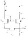
- FIG. 1 is a schematic diagram of a current-limit circuit in accordance with a first embodiment of the present invention.
- FIG. 2 is a schematic diagram of a current-limit circuit in accordance with a second embodiment of the invention.
- FIG. 3 is a top view of a cell block that can be incorporated into a semiconductor structure to form an integrated sense/power transistor structure in accordance with the invention.
- FIG. 4 is a top view of the cell block of FIG. 3, where the cells and the body region of the cell block are not shown.
- FIG. 5 is a cross-sectional view of a portion of the cell block of FIG. 3 .
- FIG. 6 is a top view of the integrated sense/power transistor structure in accordance with the invention.
- FIG. 7 is a flow diagram of a method of fabricating an integrated sense/power transistor structure in accordance with the invention.
- FIG. 8 is a flow diagram of a method of limiting the output current using a current-limit circuit in accordance with the invention.
- the current-limit circuit 10 includes a power transistor that provides the output current I O to a load.
- the current-limit circuit is designed to effectively limit the amount of the output current I O being supplied to the load in the event of a short-circuit condition.
- the current-limit circuit is designed such that the performance of the power transistor is not degraded during normal operating conditions.
- the current-limit circuit 10 includes the power transistor 12 , a current source 14 , a control transistor 16 and a switching transistor 18 .
- the transistors 12 , 16 and 18 are N-channel metal oxide semiconductor (NMOS) transistors.
- the power transistor provides a current path between a supply voltage (V DD ) rail 20 and an output terminal 22 .
- the power transistor is configured as a source follower. Thus, the drain of power transistor is connected to the V DD rail, while the source of the power transistor is connected to the output terminal.
- the output terminal 22 supplies the output current I O to the load.
- the resistance of the load is represented by a resistor 24 , which is schematically shown in FIG. 1 to be connected to the output terminal and electrical ground.
- the current source 14 and the transistors 16 and 18 are connected in series between a high voltage node 26 and the output terminal 22 .
- the voltage at the node 26 may be a voltage V CP supplied by a charge pump (not shown).
- the current source supplies the current I g to the drain and the gate of the control transistor 16 .
- the control transistor is coupled to the power transistor 12 in a current mirror configuration.
- the gate of the control transistor is coupled to the gate of the power transistor.
- the current mirror configuration of the two transistors 12 and 16 allows the output current I O to be limited by controlling the current I p drawn through the power transistor, during a short-circuit condition.
- the switching transistor 18 of the current-limit circuit 10 provides a conduction path between the control transistor 16 and the output terminal 22 .
- the drain of the switching transistor is coupled to the source of the control transistor 16 , while the source of the switching transistor is coupled to the output terminal 22 .
- the gate of the switching transistor is supplied with V DD .
- the configuration of the switching transistor is such that, under normal operating conditions, it is deactivated to a non-conductive state. Consequently, the control transistor is also deactivated to a non-conducting state. However, when the output terminal is shorted to electrical ground, the switching transistor is activated to a conducting state, which in turn activates he control transistor.
- the control transistor is activated, the current I p through the power transistor 12 is limited by the structural ratio of the control transistor and the power transistor.
- the voltage V O on the output terminal 22 is zero.
- the current source 14 provides the current I g to the gates of the power and control transistors 12 and 16 , the voltage V g at the gates of these transistors rises, which allows an increasing amount of current I p to be conducted through the power transistor 12 .
- the output voltage V O will rise to V DD ⁇ V ds,sat , where V ds,sat is the saturation voltage of the control transistor 16 .
- the switching transistor 18 is deactivated to a non-conducting state and the current I g will charge the gate of the power transistor to a level where the gate voltage V g is greater than the supply voltage V DD , which lowers the R DS of the power transistor.
- the current-limit circuit 10 will not degrade the performance of the power transistor.
- the switching transistor 18 is activated to a conducting state since the output voltage V O equals zero or near zero.
- the activation of the switching transistor allows the current I g to be conducted through the control transistor 16 . Consequently, the current I p conducted through the power transistor 12 is limited to current I limit by the structural ratio of the control transistor and the power transistor.
- the current limit (I limit ) through the power transistor can be expressed as: I limit ⁇ ( W 2 / L 2 W 1 / L 1 ) ⁇ I g ⁇ I O (Eq. 1)
- the output current I O will also be limited to the current I limit plus a small amount of current conducted through the control and switching transistors 16 and 18 .
- the current-limit circuit 10 provides a current limit protection in the event of a short-circuit condition.
- FIG. 2 a current-limit circuit 28 in accordance with a second embodiment of the invention is shown.
- the current-limit circuit includes all of the components of the current-limit circuit 10 of FIG. 1 . Therefore, the reference numerals of FIG. 1 will be used to identify the same components in FIG. 2 . Since the current-limit circuit 28 of FIG. 2 includes all of the components of the circuit 10 of FIG. 1, the current-limit circuit 28 also operates to limit the output current I O in the event of a short-circuit condition. However, the current-limit circuit 28 of FIG. 2 further includes additional components that provide an over-current protection.
- the current-limit circuit 28 includes a resistor 30 and a sense transistor 32 that are connected in series between the V DD rail 20 and the output terminal 22 .
- the resistor 30 and the sense transistor are connected in parallel to the power transistor 12 .
- One side of the resistor 30 is connected to the V DD rail, while other side of the resistor is connected to the drain of the sense transistor.
- the gate of the sense transistor is connected to the gate of the power transistor 12 , while the source of the sense transistor is connected to the output terminal.
- the sense transistor is an NMOS transistor.
- the sense transistor is sized much smaller than the power transistor. As an example, the structural ratio of the power transistor to the sense transistor may be 100:1.
- the current-limit circuit 28 also includes an over-current control device 34 and a switch 36 .
- the over-current control device control is connected to a node 38 located between the resistor 30 and the sense transistor 32 to sense the voltage at that node. This voltage is used by the over-current control device to monitor the current I p through the power transistor.
- the over-current control device is connected to the switch 36 , which provides a conduction path between the control transistor 16 and the output terminal 22 when the switch is closed.
- the over-current control device provides a control signal to the switch to open or close the switch.
- the over-current control device is configured to transmit a close signal to the switch when the voltage at the node 38 indicates that the current I p is above a prescribed threshold current level.
- the current I g is conducted through the control transistor 16 , which limits the current I p through the power transistor 12 .
- the current I p folds back to a lower current level when it exceeds the threshold current level.
- the value of the lower current level will depend on the operating point, e.g., the load condition.
- the switching transistor 18 and the switch 36 are open such that current is not conducted through the control transistor 16 to the output terminal 22 .
- the switching transistor 18 is automatically activated to a conducting state.
- the activation of the control transistor allows the current I g to flow through the control transistor, which limits the current I p conducted through the power transistor 12 .
- the over-current control device 34 transmits a close signal to the switch 36 to reduce the amount of output current I O .
- the control transistor 16 is activated to a conducting state.
- the current-limit circuit 28 provides protection from an over-current condition, as well as a short-circuit condition.
- the sense transistor 32 and the power transistor 12 are structurally integrated into a single semiconductor device, which is composed of a number of adjacent cell blocks.
- a single cell block 40 is illustrated in FIGS. 3 and 4.
- FIG. 3 is a top view of the cell block, while FIG. 4 is a simplified top view of the cell block.
- the cell block includes N ⁇ M cells, as illustrated by the squares in FIG. 3.
- a device having such a configuration is commonly known as a honeycomb structure.
- the cell block of FIG. 3 is shown to include only 7 ⁇ 7 cells, the cell block may include additional cells or fewer cells.
- Each cell of the cell block is either a source cell or drain cell of the sense transistor or the power transistor.
- the source cells are indicated in FIG. 3 by “S”, while the main drain cells are indicated by “D”.
- the two drain cells that are indicated by “ ⁇ overscore (D) ⁇ ” are dummy drain cells.
- the cell block 40 of the integrated semiconductor device also includes a body contact region 42 that is positioned around the periphery of the cell block.
- the body contact region is separated from the source and drain cells by a boundary of field oxide (FOX) region 44 , while the drain and source cells are separated from each other by a gate 46 .
- M 1 metallizations 48 , 50 , 52 and 54 Positioned over the body contact region and the source and drain cells are M 1 metallizations 48 , 50 , 52 and 54 , which are formed by patterning a layer of metal.
- the source cells are collectively connected to each other by the M 1 source metallization 50 .
- the main drain cells are connected to one of the M 1 main drain metallizations 52 , which are collectively connected by an M 2 metallization to be described below.
- the dummy drain cells are collectively connected to the M 1 dummy drain metallization 54 .
- the M 1 metallizations are more clearly identifiable in FIG. 4, where the body contact region 42 and the source, main drain and dummy drain cells are not shown.
- the source cells form the common source for the sense transistor 32 and the power transistor 12 of FIG. 2 .
- the main drain cells form the drain of the power transistor.
- the dummy drain cells ⁇ overscore (D) ⁇ can either be the drain of the sense transistor or the drain of the power transistor, depending on the connection of the M 1 dummy drain metallization 54 to an overlying M 2 metal layer. The connection of the dummy drain cells to the overlying M 2 metal layer will be described below in reference to FIG. 6 .
- FIG. 5 a cross-sectional view of a portion of the cell block 40 is shown. Illustrated in FIG. 5 are a drain cell 56 , a source cell 58 and the body contact region 42 of the cell block 40 , which are formed in a P-type substrate 60 . Each of the drain and source cells includes a heavily N-doped region within a lightly N-doped region. The body contact region is a heavily P-doped region.
- the gate 46 separates the source cell from the drain cell. The gate may be formed of a poly-silicon.
- the FOX region 44 separates the drain cell from the body contact region.
- a FOX region 62 separates the body contact region 42 from a body contact region of an adjacent cell block (not shown).
- a CVD oxide layer 64 is positioned over the body contact region and the source and drain cells.
- the CVD oxide layer includes vias 66 that allow the M 1 metallizations 48 , 50 and 52 to be in contact with the body contact region 42 , the source cell 58 , and the drain cell 56 , respectively.
- FIG. 6 illustrates the manner in which cell blocks, identical to the cell block 40 of FIG. 3, are arranged and electrically connected to form an integrated sense/power transistor device 68 .
- the integrated device includes only four cell blocks 70 , 72 , 74 and 76 .
- additional cell blocks can be included to form a larger integrated sense/power transistor device.
- the source cells, the drain cells, the dummy drain cells and the body contact regions of the cell blocks are not illustrated in FIG. 6 . Instead, only the M 1 metallizations 50 , 52 and 54 that are connected to the source cells, the drain cells and the dummy drain cells of the cell blocks are shown.
- the integrated sense/power transistor device 68 includes M 2 metallizations 78 , 80 , 82 , 84 and 86 that overlay the M 1 metallizations 50 , 52 and 54 of the cell blocks 70 , 72 , 74 and 76 .
- the M 2 source metallization 78 is connected to the M 1 source metallizations 50 , which are connected to the source cells of the cell blocks 70 - 76 .
- each source cell of the cell blocks 70 - 76 is connected to the M 2 source metallization.
- the M 2 main drain metallizations 80 and 82 are connected to the M 1 main drain metallizations 52 .
- each main drain cell of the cell blocks 70 - 76 is connected to one of the M 2 main drain metallizations 80 and 82 .
- the M 2 sense drain metallizations 84 and 86 are connected to the M 1 dummy drain metallizations 54 of the cell blocks 70 , 72 and 76 .
- the M 1 dummy drain metallization 54 of the cell block 74 is not connected to one of the M 2 sense drain metallizations. Instead, the M 1 dummy drain metallization of the cell block 74 is connected to the M 2 main drain metallization 82 . Therefore, the dummy drain cells of the cell block 74 have become a part of the drain of the power transistor, rather than a part of the drain of the sense transistor.
- the size of the resulting sense transistor of the integrated device 68 can be defined. Even with just four cell blocks, as illustrated in FIG. 6, the drain of the sense transistor can be tuned to be composed of two, four, six or eight dummy drain cells.
- the M 2 main drain metallizations 80 and 82 are shown in FIG. 6 as separate metallizations, these metallizations may be configured to be a single metallization that surrounds each of the M 2 sense drain metallizations 84 and 86 .
- the configuration of the integrated sense/power transistor device 68 provides a number of advantages.
- the integrated sense/power transistor device is a honeycomb structure that includes cells that form the common source and the two drains of a sense transistor and a power transistor.
- the FOX regions are formed to provide the desired region-to-region isolations and gates are formed within each cell block of the honeycomb structure.
- the processes for forming FOX regions and gates are well known in the art. For example, gates may be formed by patterning a thin dielectric layer and a polysilicon layer. Then, when the ion implantation steps for forming the source and drain regions are executed, the presence of the polysilicon provides self alignment of the regions.
- source, main drain and dummy drain cells are formed in a substrate. These cells are positioned such that the cell adjacent to each source cell is either a main drain cell or a dummy cell. Thus, the cells are positioned in an alternating fashion where every other cell is a source cell.
- the substrate may be a P-type substrate, where each of the source, main drain and dummy drain cells includes a heavily N-doped region within a lightly N-doped region. Steps 92 and 94 may be executed simultaneously by a single ion implantation of the selected dopant.
- a body contact region for each cell block is formed in the substrate. Preferably, each body contact region is located in the periphery of a cell block. In an alternative method, the body contact regions may be formed prior to the source, main drain and dummy drain cells.
- a first layer of metal is deposited over the cells and the body regions of the integrated sense/power transistor device.
- the deposited metal layer is then patterned to form M 1 metallizations, during step 100 .
- the first metal layer is patterned to form an M 1 source metallization, an M 1 body contact metallization, an M 1 dummy drain metallization, and a number of M 1 main drain metallizations.
- the number of M 1 main drain metallizations will depend on the number of main drain cells included in each of the cell blocks.
- an insulating layer is deposited over the first layer of metal.
- a second layer of metal is then deposited over the insulating layer, during step 104 .
- the second layer of metal is selectively patterned to form M 2 source, M 2 main drain and M 2 sense drain metallizations, where each M 2 metallization is connected to one or more M 1 metallizations.
- the patterning of the second metal layer will depend on the desired size of the sense transistor. If a larger sense transistor is desired, more dummy drain cells will be electrically connected to M 2 sense drain metallizations by connecting more M 1 dummy drain metallizations to the M 2 sense drain metallizations.
- the drain size of the sense transistor can be tuned by selectively patterning the second metal layer and selectively connecting the resulting M 2 sense drain metallizations to the M 1 dummy drain metallizations.
- a power transistor is activated to a conducting state to conduct current to an output terminal.
- a control transistor is selectively activated to a conducting state in response to a predefined condition.
- the control transistor is gate coupled to the power transistor such that the current drawn through the power transistor is limited by the structural ratio of the two transistors when current is conducted through the control transistor.
- the predefined condition is either a short-circuit condition or an over-current condition. Under normal operating conditions, the control transistor is deactivated to a non-conducting state.
- a switching transistor connected between the control transistor and the output terminal is automatically switched from a non-conducting state to a conducting state. This in turn activates the control transistor to the conducting state to limit the current conducted through the power transistor, effectively limiting the amount of output current supplied to the output terminal.
- a conduction path between the control transistor and the output terminal is closed to activate the control transistor, which reduces the current conducted through the power transistor.
- the amount of current being conducted through the power transistor is monitored by sensing a voltage on a current path that includes a resistor and a sense transistor.
Landscapes
- Engineering & Computer Science (AREA)
- Microelectronics & Electronic Packaging (AREA)
- Physics & Mathematics (AREA)
- Nonlinear Science (AREA)
- Electromagnetism (AREA)
- General Physics & Mathematics (AREA)
- Radar, Positioning & Navigation (AREA)
- Automation & Control Theory (AREA)
- Semiconductor Integrated Circuits (AREA)
Abstract
Description

Claims (20)
Priority Applications (1)
| Application Number | Priority Date | Filing Date | Title |
|---|---|---|---|
| US09/566,857 US6285177B1 (en) | 2000-05-08 | 2000-05-08 | Short-circuit current-limit circuit |
Applications Claiming Priority (1)
| Application Number | Priority Date | Filing Date | Title |
|---|---|---|---|
| US09/566,857 US6285177B1 (en) | 2000-05-08 | 2000-05-08 | Short-circuit current-limit circuit |
Publications (1)
| Publication Number | Publication Date |
|---|---|
| US6285177B1 true US6285177B1 (en) | 2001-09-04 |
Family
ID=24264686
Family Applications (1)
| Application Number | Title | Priority Date | Filing Date |
|---|---|---|---|
| US09/566,857 Expired - Lifetime US6285177B1 (en) | 2000-05-08 | 2000-05-08 | Short-circuit current-limit circuit |
Country Status (1)
| Country | Link |
|---|---|
| US (1) | US6285177B1 (en) |
Cited By (10)
| Publication number | Priority date | Publication date | Assignee | Title |
|---|---|---|---|---|
| GB2384632A (en) * | 2002-01-25 | 2003-07-30 | Zetex Plc | A power MOSFET with integrated short-circuit protection |
| US20030209764A1 (en) * | 2000-12-22 | 2003-11-13 | Matsushita Electric Industrial Co., Ltd. | Semiconductor device |
| US20040246642A1 (en) * | 2003-06-05 | 2004-12-09 | Ball Stuart R. | Protection circuit for a power switching device |
| US20050057189A1 (en) * | 2003-05-14 | 2005-03-17 | Hajime Kimura | Semiconductor device |
| US20050168905A1 (en) * | 2003-06-06 | 2005-08-04 | Hajime Kimura | Semiconductor device |
| US6977491B1 (en) | 2003-10-06 | 2005-12-20 | National Semiconductor Corporation | Current limiting voltage regulation circuit |
| US20060198572A1 (en) * | 2002-01-31 | 2006-09-07 | Sivasubramaniam Yegnanarayanan | Method to realize fast silicon-on-insulator (soi) optical device |
| US20080018310A1 (en) * | 2006-07-19 | 2008-01-24 | Dongho Lee | Detection circuitry |
| US20080253049A1 (en) * | 2007-04-16 | 2008-10-16 | Siemens Aktiengesellschaft | Circuit for load current measurement, limitation and switching |
| US8816476B2 (en) | 2011-04-27 | 2014-08-26 | Alpha & Omega Semiconductor Corporation | Through silicon via processing techniques for lateral double-diffused MOSFETS |
Citations (7)
| Publication number | Priority date | Publication date | Assignee | Title |
|---|---|---|---|---|
| US4543494A (en) | 1981-12-29 | 1985-09-24 | Fujitsu Limited | MOS type output driver circuit having a protective circuit |
| US4612497A (en) | 1985-09-13 | 1986-09-16 | Motorola, Inc. | MOS current limiting output circuit |
| US4709171A (en) * | 1982-05-27 | 1987-11-24 | Motorola, Inc. | Current limiter and method for limiting current |
| US4771228A (en) | 1987-06-05 | 1988-09-13 | Vtc Incorporated | Output stage current limit circuit |
| US5386336A (en) * | 1992-06-19 | 1995-01-31 | Trw Inc. | On chip current limiter |
| US5579193A (en) | 1994-06-24 | 1996-11-26 | Texas Instruments Incorporated | Reducing the natural current limit in a power MOS device by reducing the gate-source voltage |
| US6002288A (en) * | 1996-12-13 | 1999-12-14 | Texas Instruments Incorporated | Current limiting circuit and method that may be shared among different circuitry |
-
2000
- 2000-05-08 US US09/566,857 patent/US6285177B1/en not_active Expired - Lifetime
Patent Citations (7)
| Publication number | Priority date | Publication date | Assignee | Title |
|---|---|---|---|---|
| US4543494A (en) | 1981-12-29 | 1985-09-24 | Fujitsu Limited | MOS type output driver circuit having a protective circuit |
| US4709171A (en) * | 1982-05-27 | 1987-11-24 | Motorola, Inc. | Current limiter and method for limiting current |
| US4612497A (en) | 1985-09-13 | 1986-09-16 | Motorola, Inc. | MOS current limiting output circuit |
| US4771228A (en) | 1987-06-05 | 1988-09-13 | Vtc Incorporated | Output stage current limit circuit |
| US5386336A (en) * | 1992-06-19 | 1995-01-31 | Trw Inc. | On chip current limiter |
| US5579193A (en) | 1994-06-24 | 1996-11-26 | Texas Instruments Incorporated | Reducing the natural current limit in a power MOS device by reducing the gate-source voltage |
| US6002288A (en) * | 1996-12-13 | 1999-12-14 | Texas Instruments Incorporated | Current limiting circuit and method that may be shared among different circuitry |
Cited By (26)
| Publication number | Priority date | Publication date | Assignee | Title |
|---|---|---|---|---|
| US20030209764A1 (en) * | 2000-12-22 | 2003-11-13 | Matsushita Electric Industrial Co., Ltd. | Semiconductor device |
| US6838736B2 (en) * | 2000-12-22 | 2005-01-04 | Matsushita Electric Industrial Co., Ltd. | Semiconductor device having noise immunity |
| GB2384632B (en) * | 2002-01-25 | 2005-11-16 | Zetex Plc | Current limiting protection circuit |
| US20030169025A1 (en) * | 2002-01-25 | 2003-09-11 | Zetex Plc | Current limiting protection circuit |
| US6778366B2 (en) | 2002-01-25 | 2004-08-17 | Zetex Plc | Current limiting protection circuit |
| GB2384632A (en) * | 2002-01-25 | 2003-07-30 | Zetex Plc | A power MOSFET with integrated short-circuit protection |
| US20060198572A1 (en) * | 2002-01-31 | 2006-09-07 | Sivasubramaniam Yegnanarayanan | Method to realize fast silicon-on-insulator (soi) optical device |
| EP1624358A4 (en) * | 2003-05-14 | 2008-01-23 | Semiconductor Energy Lab | Semiconductor device |
| EP2299429A1 (en) * | 2003-05-14 | 2011-03-23 | Semiconductor Energy Laboratory Co, Ltd. | Semiconductor device |
| US9576526B2 (en) | 2003-05-14 | 2017-02-21 | Semiconductor Energy Laboratory Co., Ltd. | Semiconductor device |
| US8289238B2 (en) | 2003-05-14 | 2012-10-16 | Semiconductor Energy Laboratory Co., Ltd. | Semiconductor device |
| US20050057189A1 (en) * | 2003-05-14 | 2005-03-17 | Hajime Kimura | Semiconductor device |
| US7463223B2 (en) | 2003-05-14 | 2008-12-09 | Semiconductor Energy Laboratory Co., Ltd. | Semiconductor device |
| US20040246642A1 (en) * | 2003-06-05 | 2004-12-09 | Ball Stuart R. | Protection circuit for a power switching device |
| US7046494B2 (en) | 2003-06-05 | 2006-05-16 | Seagate Technology Llc | Protection circuit for a power switching device |
| US8284128B2 (en) | 2003-06-06 | 2012-10-09 | Semiconductor Energy Laboratory Co., Ltd. | Semiconductor device |
| US7852330B2 (en) | 2003-06-06 | 2010-12-14 | Semiconductor Energy Laboratory Co., Ltd. | Semiconductor device |
| US20050168905A1 (en) * | 2003-06-06 | 2005-08-04 | Hajime Kimura | Semiconductor device |
| US20110133828A1 (en) * | 2003-06-06 | 2011-06-09 | Semiconductor Energy Laboratory Co., Ltd. | Semiconductor Device |
| US6977491B1 (en) | 2003-10-06 | 2005-12-20 | National Semiconductor Corporation | Current limiting voltage regulation circuit |
| US7869177B2 (en) | 2006-07-19 | 2011-01-11 | Hewlett-Packard Development Company, L.P. | Detection circuitry |
| US20080018310A1 (en) * | 2006-07-19 | 2008-01-24 | Dongho Lee | Detection circuitry |
| EP1983348A1 (en) * | 2007-04-16 | 2008-10-22 | Siemens Aktiengesellschaft | Circuit for measuring, limiting and switching a load current |
| US7639468B2 (en) | 2007-04-16 | 2009-12-29 | Siemens Aktiengesellschaft | Circuit for load current measurement, limitation and switching |
| US20080253049A1 (en) * | 2007-04-16 | 2008-10-16 | Siemens Aktiengesellschaft | Circuit for load current measurement, limitation and switching |
| US8816476B2 (en) | 2011-04-27 | 2014-08-26 | Alpha & Omega Semiconductor Corporation | Through silicon via processing techniques for lateral double-diffused MOSFETS |
Similar Documents
| Publication | Publication Date | Title |
|---|---|---|
| US20240297499A1 (en) | Esd protection circuit | |
| JP2698645B2 (en) | MOSFET | |
| US5025298A (en) | Semiconductor structure with closely coupled substrate temperature sense element | |
| US6855586B2 (en) | Low voltage breakdown element for ESD trigger device | |
| US7851889B2 (en) | MOSFET device including a source with alternating P-type and N-type regions | |
| US20090108346A1 (en) | Hybrid-mode ldmos | |
| EP2472586A1 (en) | Thin Film Metal-Dielectric-Metal Transistor | |
| US5600160A (en) | Multichannel field effect device | |
| US20020096709A1 (en) | Semiconductor switching device and method | |
| US6285177B1 (en) | Short-circuit current-limit circuit | |
| JPH0864812A (en) | Overvoltage protection semiconductor switch | |
| JP7147970B2 (en) | Trimming circuit and trimming method | |
| US6621138B1 (en) | Zener-like trim device in polysilicon | |
| JP3660566B2 (en) | Overcurrent limiting semiconductor device | |
| CN100543999C (en) | CMOS semiconductor device and manufacturing method thereof | |
| GB2384632A (en) | A power MOSFET with integrated short-circuit protection | |
| US5969923A (en) | Electrostatic protection structure for MOS circuits | |
| EP0601823A1 (en) | Field effect transistor with integrated schottky diode clamp | |
| JPH1065146A (en) | Semiconductor integrated circuit device | |
| JPH04170815A (en) | High side switch circuit and semiconductor device | |
| US6774440B1 (en) | Semiconductor device and method for driving the same | |
| JP2002176347A (en) | Overcurrent limiting semiconductor device | |
| KR0175402B1 (en) | Power semiconductor device and manufacturing method | |
| JP2604628B2 (en) | Bidirectional switching device | |
| JP2780289B2 (en) | Semiconductor device |
Legal Events
| Date | Code | Title | Description |
|---|---|---|---|
| AS | Assignment |
Owner name: IMPALA LINEAR CORPORATION, CALIFORNIA Free format text: ASSIGNMENT OF ASSIGNORS INTEREST;ASSIGNORS:MALLIKARJUNASWAMY, SHEKAR;FLOYD, BRIAN H.;REEL/FRAME:010792/0886;SIGNING DATES FROM 20000420 TO 20000428 |
|
| AS | Assignment |
Owner name: VENTURE BANKING GROUP, CALIFORNIA Free format text: SECURITY INTEREST;ASSIGNOR:IMPALA LINEAR CORPORATION;REEL/FRAME:010984/0385 Effective date: 20000613 |
|
| STCF | Information on status: patent grant |
Free format text: PATENTED CASE |
|
| AS | Assignment |
Owner name: FAIRCHILD SEMICONDUCTOR CORPORATION, MAINE Free format text: MERGER;ASSIGNOR:IMPALA LINEAR CORPORATION;REEL/FRAME:013110/0540 Effective date: 20010905 |
|
| FPAY | Fee payment |
Year of fee payment: 4 |
|
| FPAY | Fee payment |
Year of fee payment: 8 |
|
| FPAY | Fee payment |
Year of fee payment: 12 |
|
| AS | Assignment |
Owner name: DEUTSCHE BANK AG NEW YORK BRANCH, AS COLLATERAL AGENT, NEW YORK Free format text: PATENT SECURITY AGREEMENT;ASSIGNOR:FAIRCHILD SEMICONDUCTOR CORPORATION;REEL/FRAME:040075/0644 Effective date: 20160916 Owner name: FAIRCHILD SEMICONDUCTOR CORPORATION, CALIFORNIA Free format text: RELEASE BY SECURED PARTY;ASSIGNOR:WELLS FARGO BANK, NATIONAL ASSOCIATION;REEL/FRAME:040073/0131 Effective date: 20160915 Owner name: DEUTSCHE BANK AG NEW YORK BRANCH, AS COLLATERAL AG Free format text: PATENT SECURITY AGREEMENT;ASSIGNOR:FAIRCHILD SEMICONDUCTOR CORPORATION;REEL/FRAME:040075/0644 Effective date: 20160916 |
|
| AS | Assignment |
Owner name: FAIRCHILD SEMICONDUCTOR CORPORATION, CALIFORNIA Free format text: CORRECTIVE ASSIGNMENT TO CORRECT THE INCORRECT PATENT NUMBER 5002244 PREVIOUSLY RECORDED ON REEL 040073 FRAME 0131. ASSIGNOR(S) HEREBY CONFIRMS THE RELEASE OF SECURED INTEREST;ASSIGNOR:WELLS FARGO BANK, NATIONAL ASSOCIATION;REEL/FRAME:040477/0663 Effective date: 20160915 |
|
| AS | Assignment |
Owner name: FAIRCHILD SEMICONDUCTOR CORPORATION, ARIZONA Free format text: RELEASE BY SECURED PARTY;ASSIGNOR:DEUTSCHE BANK AG NEW YORK BRANCH;REEL/FRAME:057969/0206 Effective date: 20211027 Owner name: FAIRCHILD SEMICONDUCTOR CORPORATION, ARIZONA Free format text: RELEASE OF SECURITY INTEREST;ASSIGNOR:DEUTSCHE BANK AG NEW YORK BRANCH;REEL/FRAME:057969/0206 Effective date: 20211027 |
|
| AS | Assignment |
Owner name: DEUTSCHE BANK AG NEW YORK BRANCH, AS COLLATERAL AGENT, NEW YORK Free format text: SECURITY INTEREST;ASSIGNOR:SEMICONDUCTOR COMPONENTS INDUSTRIES, LLC;REEL/FRAME:058871/0799 Effective date: 20211028 |
|
| AS | Assignment |
Owner name: FAIRCHILD SEMICONDUCTOR CORPORATION, ARIZONA Free format text: RELEASE OF SECURITY INTEREST IN PATENTS RECORDED AT REEL 040075, FRAME 0644;ASSIGNOR:DEUTSCHE BANK AG NEW YORK BRANCH, AS COLLATERAL AGENT;REEL/FRAME:064070/0536 Effective date: 20230622 Owner name: SEMICONDUCTOR COMPONENTS INDUSTRIES, LLC, ARIZONA Free format text: RELEASE OF SECURITY INTEREST IN PATENTS RECORDED AT REEL 040075, FRAME 0644;ASSIGNOR:DEUTSCHE BANK AG NEW YORK BRANCH, AS COLLATERAL AGENT;REEL/FRAME:064070/0536 Effective date: 20230622 |
|
| AS | Assignment |
Owner name: FAIRCHILD SEMICONDUCTOR CORPORATION, ARIZONA Free format text: RELEASE OF SECURITY INTEREST IN PATENTS RECORDED AT REEL 058871, FRAME 0799;ASSIGNOR:DEUTSCHE BANK AG NEW YORK BRANCH, AS COLLATERAL AGENT;REEL/FRAME:065653/0001 Effective date: 20230622 Owner name: SEMICONDUCTOR COMPONENTS INDUSTRIES, LLC, ARIZONA Free format text: RELEASE OF SECURITY INTEREST IN PATENTS RECORDED AT REEL 058871, FRAME 0799;ASSIGNOR:DEUTSCHE BANK AG NEW YORK BRANCH, AS COLLATERAL AGENT;REEL/FRAME:065653/0001 Effective date: 20230622 |