US6175127B1 - Stack capacitor having a diffusion barrier - Google Patents

Stack capacitor having a diffusion barrier Download PDF

Info

Publication number
US6175127B1
US6175127B1 US09/349,492 US34949299A US6175127B1 US 6175127 B1 US6175127 B1 US 6175127B1 US 34949299 A US34949299 A US 34949299A US 6175127 B1 US6175127 B1 US 6175127B1
Authority
US
United States
Prior art keywords
diffusion barrier
lower electrode
contact plug
stack capacitor
barrier layer
Prior art date
Legal status (The legal status is an assumption and is not a legal conclusion. Google has not performed a legal analysis and makes no representation as to the accuracy of the status listed.)
Expired - Lifetime
Application number
US09/349,492
Inventor
Suk Kyoung Hong
Current Assignee (The listed assignees may be inaccurate. Google has not performed a legal analysis and makes no representation or warranty as to the accuracy of the list.)
SK Hynix Inc
Original Assignee
Hyundai Electronics Industries Co Ltd
Priority date (The priority date is an assumption and is not a legal conclusion. Google has not performed a legal analysis and makes no representation as to the accuracy of the date listed.)
Filing date
Publication date
Application filed by Hyundai Electronics Industries Co Ltd filed Critical Hyundai Electronics Industries Co Ltd
Assigned to HYUNDAI ELECTRONICS INDUSTRIES CO., LTD. reassignment HYUNDAI ELECTRONICS INDUSTRIES CO., LTD. ASSIGNMENT OF ASSIGNORS INTEREST (SEE DOCUMENT FOR DETAILS). Assignors: HONG, SUK KYOUNG
Application granted granted Critical
Publication of US6175127B1 publication Critical patent/US6175127B1/en
Anticipated expiration legal-status Critical
Expired - Lifetime legal-status Critical Current

Links

Images

Classifications

    • HELECTRICITY
    • H10SEMICONDUCTOR DEVICES; ELECTRIC SOLID-STATE DEVICES NOT OTHERWISE PROVIDED FOR
    • H10DINORGANIC ELECTRIC SEMICONDUCTOR DEVICES
    • H10D84/00Integrated devices formed in or on semiconductor substrates that comprise only semiconducting layers, e.g. on Si wafers or on GaAs-on-Si wafers
    • HELECTRICITY
    • H10SEMICONDUCTOR DEVICES; ELECTRIC SOLID-STATE DEVICES NOT OTHERWISE PROVIDED FOR
    • H10DINORGANIC ELECTRIC SEMICONDUCTOR DEVICES
    • H10D1/00Resistors, capacitors or inductors
    • H10D1/60Capacitors
    • H10D1/68Capacitors having no potential barriers
    • H10D1/692Electrodes
    • HELECTRICITY
    • H10SEMICONDUCTOR DEVICES; ELECTRIC SOLID-STATE DEVICES NOT OTHERWISE PROVIDED FOR
    • H10BELECTRONIC MEMORY DEVICES
    • H10B12/00Dynamic random access memory [DRAM] devices
    • H10B12/30DRAM devices comprising one-transistor - one-capacitor [1T-1C] memory cells
    • H10B12/31DRAM devices comprising one-transistor - one-capacitor [1T-1C] memory cells having a storage electrode stacked over the transistor
    • H10B12/315DRAM devices comprising one-transistor - one-capacitor [1T-1C] memory cells having a storage electrode stacked over the transistor with the capacitor higher than a bit line

Definitions

  • the present invention relates to a highly integrated memory device having a stack capacitor structure in which a transistor and a capacitor included in each cell of the memory device are coupled to each other by a polysilicon contact plug in order to achieve an increase in the cell integration degree of the memory device, and more particularly to a stack capacitor in such a memory device, wherein a capacitor has a diffusion barrier capable of inhibiting an oxidation of the polysilicon contact plug while preventing an increase in contact resistance resulting from a reaction of the polysilicon of the contact plug with a lower electrode.
  • FIG. 1 there is a sectional view schematically illustrating a simple stack capacitor used in a conventional DRAM device.
  • a lower insulating layer 13 which has storage electrode contact holes 15 , is formed over a semiconductor substrate 11 .
  • Polysilicon is buried in the contact holes 15 , thereby forming contact plugs 17 .
  • a diffusion barrier layer 19 and a lower electrode layer for forming lower electrodes 21 are sequentially formed to desired thicknesses over the entire upper surface of the resulting structure.
  • the lower electrode layer and diffusion barrier layer 19 are then patterned in accordance with an etch process using a storage electrode mask (not shown), thereby forming diffusion barriers 19 and lower electrodes 21 .
  • a dielectric film 23 and a plate electrode layer for forming plate electrodes 25 as upper electrodes are then formed.
  • stack capacitors are fabricated.
  • the stack capacitors are electrically connected to transistors formed on the semiconductor substrate 11 via the contact plugs 17 , respectively.
  • the dielectric film 23 is made of a paraelectric or ferroelectric substance exhibiting a very high dielectric constant.
  • a paraelectric or ferroelectric substance may be SrTiO 3 (ST), (Ba x , Sr 1 ⁇ x )TiO 3 (BST), Pb(Zr x , Ti 1 ⁇ x )O 3 (PZT), or (Pb 1 ⁇ y , Lay) (Zr x Ti 1 ⁇ x )O 3 (PLZT)
  • such a high-dielectric thin film should be deposited or annealed in an oxygen atmosphere maintained at a high temperature of 500 to 800° C. so that it exhibits a desired dielectric constant and leakage current characteristics.
  • a metal such as Pt, Ir or Ru or a conductive oxide such as IrO 2 or RuO 2 is typically used which exhibits a superior electrical conductivity and superior thermal resistance and anti-oxidation characteristics is typically used.
  • the above-mentioned high-dielectric thin film made of, for example, ST, BST, PZT or PLZT is deposited in an oxygen atmosphere at a high temperature, oxygen may be easily diffused through the lower electrodes of the capacitors, so that it may react with the polysilicon of the contact plugs. As a result, an insulating layer such as a silicon oxide film may be formed at the interface of the polysilicon with the lower electrodes. That is, there is a problem in that an undesirable electrical insulation is established.
  • Si may also be diffused into the lower electrodes. Such a diffusion of Si may result in a degradation in the physical properties of the deposited high-dielectric thin film.
  • a diffusion barrier layer is typically disposed between the lower electrodes of the stack capacitors and the Si layer.
  • such a diffusion barrier layer is mainly made of TiN having a resistivity while exhibiting superior diffusion barrier characteristics at a temperature of 600° C. or less.
  • TiN loses its diffusion barrier effect to oxygen and Si in an oxygen atmosphere maintained at a high temperature of more than 600° C. For this reason, TiN serves to greatly limit processing conditions including the deposition temperature of the high-dielectric thin film and the temperature of a subsequent thermal treatment.
  • an objective of the invention is to solve the above mentioned problems involved in the prior art and to provide a stack capacitor having a diffusion barrier capable of inhibiting an oxidation of a polysilicon contact plug adapted to connect the stack capacitor to a transistor and preventing the interaction between the polysilicon of the contact plug and a lower electrode included in the stack capacitor.
  • a stack capacitor comprises a lower electrode connected to a semiconductor substrate via a polysilicon contact plug; a diffusion barrier layer formed at an interface between the contact plug and the lower electrode, the diffusion barrier layer being made of a material of Ti 1 ⁇ x Cr x N ( 0 ⁇ x ⁇ 1 ); and a dielectric film and an upper electrode sequentially formed over a surface of the lower electrode opposite to the interface.
  • FIG. 1 is a sectional view illustrating a simple stack capacitor having a conventional structure
  • FIG. 2 is a graph depicting a variation in the oxidation rate constant at a temperature of 600° C., depending on the content of Cr in a Ti 1 ⁇ x Cr x N diffusion barrier in accordance with an embodiment of the present invention.
  • a TiN thin film which has been widely used in highly integrated DRAMs for a diffusion barrier layer interposed between a stack capacitor and a polysilicon contact plug, conducts an oxidation of “TiN+1/20 2 ⁇ TiO+N ⁇ ” when it is subjected to a thermal treatment in an oxygen atmosphere at a high temperature of about 600° C. or more, thereby forming a thin oxide layer of TiO.
  • the contact resistance of the contact plug which serves as an electrical connection channel of the capacitor with a transistor, may greatly increase. In severe cases, an undesirable electrical insulation may occur.
  • bubbles are formed at the interface of the contact plug with a lower electrode (made of, for example, Pt) included in the capacitor due to a generation of N 2 gas. As a result, the structure of the stack capacitor may be damaged.
  • the oxidation rate constant “k′(T)” has a relationship with the self diffusion coefficient of ions in the oxide layer and is determined by the activation energy “Ea” and the diffusivity prefactor “k 0 ”.
  • the nitride of Ti 1 ⁇ x Cr x N ( 0 ⁇ x ⁇ 1 ) which is a solid solution of TiN and CrN exhibits a variation in the reaction rate constant “k′” and a variation in resistivity, depending on the Cr content “x” therein.
  • k′ reaction rate constant
  • resistivity resistivity
  • FIG. 2 a graph is illustrated which depicts a variation in the oxidation rate constant at a temperature of 600° C., depending on the content of Cr in a Ti 1 ⁇ x Cr x N diffusion barrier in accordance with an embodiment of the present invention.
  • the simple stack capacitor which has a Ti 1 ⁇ x Cr x N diffusion barrier in accordance with the present invention, has the same structure as that shown in FIG. 1, except that the diffusion barrier is made of Ti 1 ⁇ x Cr x N.
  • the deposition of the Ti 1 ⁇ x Cr x N ( 0 ⁇ x ⁇ 1 ) thin film to be used as the diffusion barrier is carried out using a DC reactive sputtering process which is widely used for a metal wiring deposition in an Si semiconductor process.
  • metal targets of Ti and Cr are used.
  • the Cr content “x” in the composition of “Ti 1 ⁇ x Cr x N” can be easily adjusted by adjusting the mixture ratio of Ar and N 2 used as sputtering gas, the DC power applied to the Ti and Cr targets, and the distance between the substrate and each target, and the temperature of the substrate.
  • the Ti 1 ⁇ x Cr x N ( 0 ⁇ x ⁇ 1 ) thin film is thermally treated at a temperature of about 600° C. in the atmosphere so that it is oxidized.
  • the thickness of the resulting oxide film can be measured by measuring the distribution of elements constituting the oxide film in the film thickness direction using an Auger electron spectroscopy.
  • the thickness “d ox ” of the oxide film can be expressed, in accordance with the parabolic oxidation law, as follows:
  • the thickness dox of the oxide film measured as mentioned above is depicted with respect to the oxidation time “t”, it has the form of a straight line. Based on the gradient of this straight line, it is possible to calculate the oxidation rate constant “k′”.
  • the oxidation rate constant “k′” of the Ti 1 ⁇ x Cr x N thin film decreases greatly at a rate corresponding to 1/100 to 1/1,000 of the oxidation rate constant of TiN as the Cr content “x” increases from 0 to 1.
  • the resistivity of the Ti 1 ⁇ x Cr x N thin film increases in the form of a straight line as the Cr content “x” increases.
  • a nitride film of Ti 1 ⁇ x Cr x N in which the Cr content “x” ranges between 0.2 and 0.7 ( 0 . 2 ⁇ x ⁇ 0 . 7 ), is suitable for the diffusion barrier.
  • the stack capacitor having a diffusion barrier according to the present invention provides various effects.
  • the Ti 1 ⁇ x Cr x N ( 0 ⁇ x ⁇ 1 ) thin film is used as a diffusion barrier film in accordance with the present invention, it is possible to inhibit an oxidation of a plug connecting the capacitor to a transistor while preventing a reaction of silicon with a lower electrode included in the capacitor.
  • the diffusion barrier film of the present invention also exhibits a considerably low resistivity as compared to the polysilicon contact plug. Accordingly, the diffusion barrier film of the present invention is suitable for use in a ULSI DRAM having a stack capacitor structure.

Landscapes

  • Semiconductor Memories (AREA)
  • Electrodes Of Semiconductors (AREA)
  • Semiconductor Integrated Circuits (AREA)

Abstract

A stack capacitor including a lower electrode connected to a semiconductor substrate via a polysilicon contact plug, a diffusion barrier layer formed at an interface between the contact plug and the lower electrode, the diffusion barrier layer being made of a material of Ti1-xCrxN (0<=x<=1), and a dielectric film and an upper electrode sequentially formed over a surface of the lower electrode opposite to the interface. The diffusion barrier serves to inhibit an oxidation of the polysilicon contact plug while preventing an increase in contact resistance resulting from a reaction of the polysilicon of the contact plug with the lower electrode. The dielectric film is comprised of a high-dielectric thin film so that it provides, to the capacitor, a sufficient capacitance for a high integration of a semiconductor device. The lower electrode is made of a material exhibiting superior electrical conductivity, thermal resistance and anti-oxidation characteristics. The stack capacitor achieves a high integration of semiconductor devices and an improvement in the characteristics and reliability of those semiconductor devices.

Description

BACKGROUND OF THE INVENTION
1. Field of the Invention
The present invention relates to a highly integrated memory device having a stack capacitor structure in which a transistor and a capacitor included in each cell of the memory device are coupled to each other by a polysilicon contact plug in order to achieve an increase in the cell integration degree of the memory device, and more particularly to a stack capacitor in such a memory device, wherein a capacitor has a diffusion barrier capable of inhibiting an oxidation of the polysilicon contact plug while preventing an increase in contact resistance resulting from a reaction of the polysilicon of the contact plug with a lower electrode.
2. Description of the Prior Art
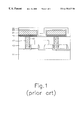
Referring to FIG. 1, there is a sectional view schematically illustrating a simple stack capacitor used in a conventional DRAM device.
As shown in FIG. 1, a lower insulating layer 13, which has storage electrode contact holes 15, is formed over a semiconductor substrate 11. Polysilicon is buried in the contact holes 15, thereby forming contact plugs 17.
Thereafter, a diffusion barrier layer 19 and a lower electrode layer for forming lower electrodes 21 are sequentially formed to desired thicknesses over the entire upper surface of the resulting structure.
The lower electrode layer and diffusion barrier layer 19 are then patterned in accordance with an etch process using a storage electrode mask (not shown), thereby forming diffusion barriers 19 and lower electrodes 21.
Over the entire upper surface of the resulting structure, a dielectric film 23 and a plate electrode layer for forming plate electrodes 25 as upper electrodes are then formed. Thus, stack capacitors are fabricated.
The stack capacitors are electrically connected to transistors formed on the semiconductor substrate 11 via the contact plugs 17, respectively.
The dielectric film 23 is made of a paraelectric or ferroelectric substance exhibiting a very high dielectric constant. Such a paraelectric or ferroelectric substance may be SrTiO3 (ST), (Bax, Sr1−x)TiO3 (BST), Pb(Zrx, Ti1−x)O3 (PZT), or (Pb1−y, Lay) (ZrxTi1−x)O3 (PLZT)
Typically, such a high-dielectric thin film should be deposited or annealed in an oxygen atmosphere maintained at a high temperature of 500 to 800° C. so that it exhibits a desired dielectric constant and leakage current characteristics.
For the material of electrodes used in simple stack capacitors including dielectric films exhibiting a high electric constant, accordingly, a metal such as Pt, Ir or Ru or a conductive oxide such as IrO2 or RuO2 is typically used which exhibits a superior electrical conductivity and superior thermal resistance and anti-oxidation characteristics is typically used.
However, since the above-mentioned high-dielectric thin film made of, for example, ST, BST, PZT or PLZT is deposited in an oxygen atmosphere at a high temperature, oxygen may be easily diffused through the lower electrodes of the capacitors, so that it may react with the polysilicon of the contact plugs. As a result, an insulating layer such as a silicon oxide film may be formed at the interface of the polysilicon with the lower electrodes. That is, there is a problem in that an undesirable electrical insulation is established.
Meanwhile, Si may also be diffused into the lower electrodes. Such a diffusion of Si may result in a degradation in the physical properties of the deposited high-dielectric thin film.
Furthermore, when the material of the lower electrodes of the capacitors come into direct contact with the polysilicon, a reaction between these two materials may occur at a high temperature of 200° C. or more, thereby producing PtSi exhibiting Schottky barrier characteristics. This results in a degradation in CMOS characteristics.
In order to inhibit an oxidizing diffusion of oxygen and Si atoms while preventing Si from coming into direct contact with the lower electrodes, a diffusion barrier layer is typically disposed between the lower electrodes of the stack capacitors and the Si layer.
In a highly integrated DRAM, such a diffusion barrier layer is mainly made of TiN having a resistivity while exhibiting superior diffusion barrier characteristics at a temperature of 600° C. or less.
However, TiN loses its diffusion barrier effect to oxygen and Si in an oxygen atmosphere maintained at a high temperature of more than 600° C. For this reason, TiN serves to greatly limit processing conditions including the deposition temperature of the high-dielectric thin film and the temperature of a subsequent thermal treatment.
SUMMARY OF THE INVENTION
Therefore, an objective of the invention is to solve the above mentioned problems involved in the prior art and to provide a stack capacitor having a diffusion barrier capable of inhibiting an oxidation of a polysilicon contact plug adapted to connect the stack capacitor to a transistor and preventing the interaction between the polysilicon of the contact plug and a lower electrode included in the stack capacitor.
In accordance with the present invention, a stack capacitor comprises a lower electrode connected to a semiconductor substrate via a polysilicon contact plug; a diffusion barrier layer formed at an interface between the contact plug and the lower electrode, the diffusion barrier layer being made of a material of Ti1−xCrxN (0≦x≦1); and a dielectric film and an upper electrode sequentially formed over a surface of the lower electrode opposite to the interface.
BRIEF DESCRIPTION OF THE DRAWINGS
Other objectives and aspects of the invention will become apparent from the following description of embodiments with reference to the accompanying drawings in which:
FIG. 1 is a sectional view illustrating a simple stack capacitor having a conventional structure; and
FIG. 2 is a graph depicting a variation in the oxidation rate constant at a temperature of 600° C., depending on the content of Cr in a Ti1−xCrxN diffusion barrier in accordance with an embodiment of the present invention.
DESCRIPTION OF THE PREFERRED EMBODIMENTS
Prior to the description of the preferred embodiments of the present invention, the principle of the present invention will be described.
A TiN thin film, which has been widely used in highly integrated DRAMs for a diffusion barrier layer interposed between a stack capacitor and a polysilicon contact plug, conducts an oxidation of “TiN+1/202→TiO+N↑” when it is subjected to a thermal treatment in an oxygen atmosphere at a high temperature of about 600° C. or more, thereby forming a thin oxide layer of TiO.
As a result, the contact resistance of the contact plug, which serves as an electrical connection channel of the capacitor with a transistor, may greatly increase. In severe cases, an undesirable electrical insulation may occur.
Furthermore, bubbles are formed at the interface of the contact plug with a lower electrode (made of, for example, Pt) included in the capacitor due to a generation of N2 gas. As a result, the structure of the stack capacitor may be damaged.
The oxidation of the nitride thin film, which is widely used as a diffusion barrier layer, is a thermally active reaction. Accordingly, this oxidation may be expressed by the Arrhenious equation having a temperature dependency of “k′(T)=k0 exp(−Ea/kT)” (here, “k” represents a Boltzmann constant, “T” represents an oxidation temperature, and “Ea” represents energy activating the oxidation).
In accordance with the Wagner theory associated with a parabolic oxidation, the oxidation rate constant “k′(T)” has a relationship with the self diffusion coefficient of ions in the oxide layer and is determined by the activation energy “Ea” and the diffusivity prefactor “k0”.
Based on the comparison between “Ea” and “k0”, it is possible to select one of the various nitrides exhibiting superior electrical conductivity characteristics so that it is used for a diffusion barrier material for stack capacitors in a ULSI DRAM having a polysilicon plug structure. Based on the result of the selection, diffusion barriers are formed using the selected nitride. Thus, capacitors having the diffusion barriers made of a desired material are formed.
The following Table 1 describes the values of “Ea” and “k0” associated with various nitrides.
TABLE 1
Activation Energy Diffusivity Prefactor
Nitride Film (Ea (eV)) (k0(μg/cm4s))
TiN 1.6-1.89 0.12-1.55 × 10¹⁰
ZrN 1.83-2.37 1.39 × 10¹⁰-4.35 × 10¹²
CrN 1.92 1.83 × 10⁸
Ti0.63Zr0.37N 1.04 9.2 × 10⁵
Cr0.72Ti0.28N 3.98-4.11 1.71 × 10¹⁵-7.42 × 10¹⁸
TiN/CrN 2.91 3.58 × 10¹³
ZrN/CrN <1.0
As is apparent from Table 1, the nitride of Cr0.72Ti0.28N exhibits considerably high values of “Ea” and “k0”, as compared to TiN.
The nitride of Ti1−xCrxN (0≦x≦1) which is a solid solution of TiN and CrN exhibits a variation in the reaction rate constant “k′” and a variation in resistivity, depending on the Cr content “x” therein. In order to use this nitride of Ti1−xCrxN as a diffusion barrier material for a ULSI DRAM, it is necessary to determine an appropriate Cr content, taking into consideration the above two physical properties.
Now, a preferred embodiment of the present invention will be described in conjunction with a simple stack capacitor having a diffusion barrier made of Ti1−xCrxN.
Referring to FIG. 2, a graph is illustrated which depicts a variation in the oxidation rate constant at a temperature of 600° C., depending on the content of Cr in a Ti1−xCrxN diffusion barrier in accordance with an embodiment of the present invention.
The simple stack capacitor, which has a Ti1−xCrxN diffusion barrier in accordance with the present invention, has the same structure as that shown in FIG. 1, except that the diffusion barrier is made of Ti1−xCrxN.
The deposition of the Ti1−xCrxN (0≦x≦1) thin film to be used as the diffusion barrier is carried out using a DC reactive sputtering process which is widely used for a metal wiring deposition in an Si semiconductor process.
In accordance with the DC reactive sputtering process, metal targets of Ti and Cr are used. In this case, the Cr content “x” in the composition of “Ti1−xCrxN” can be easily adjusted by adjusting the mixture ratio of Ar and N2 used as sputtering gas, the DC power applied to the Ti and Cr targets, and the distance between the substrate and each target, and the temperature of the substrate.
After the deposition, the Ti1−xCrxN (0≦x≦1) thin film is thermally treated at a temperature of about 600° C. in the atmosphere so that it is oxidized.
The thickness of the resulting oxide film can be measured by measuring the distribution of elements constituting the oxide film in the film thickness direction using an Auger electron spectroscopy.
The thickness “dox” of the oxide film can be expressed, in accordance with the parabolic oxidation law, as follows:
d ox={square root over (2k′t)}
When the thickness dox of the oxide film measured as mentioned above is depicted with respect to the oxidation time “t”, it has the form of a straight line. Based on the gradient of this straight line, it is possible to calculate the oxidation rate constant “k′”.
By referring to FIG. 2, it can be found that the oxidation rate constant “k′” of the Ti1−xCrxN thin film decreases greatly at a rate corresponding to 1/100 to 1/1,000 of the oxidation rate constant of TiN as the Cr content “x” increases from 0 to 1.
In order to use the selected nitride for the diffusion barrier of the ULSI DRAM, it is also necessary to take into consideration the resistivity of the nitride thin film, in addition to the oxidation rate constant.
The resistivity of the Ti1−xCrxN thin film increases in the form of a straight line as the Cr content “x” increases. Taking into consideration both the oxidation rate and resistivity, accordingly, a nitride film of Ti1−xCrxN, in which the Cr content “x” ranges between 0.2 and 0.7 (0.2≦x≦0.7), is suitable for the diffusion barrier.
As is apparent from the above description, the stack capacitor having a diffusion barrier according to the present invention provides various effects.
That is, there are various advantages in regard to manufacturing processes in that the deposition and thermal treatment temperature ranges for a high-dielectric film to be formed can greatly increase because a thin film of Ti1−xCrxN (0≦x≦1) exhibiting superior anti-oxidation characteristics over the conventional TiN film is used as a diffusion barrier film in accordance with the present invention.
Since the Ti1−xCrxN (0≦x≦1) thin film is used as a diffusion barrier film in accordance with the present invention, it is possible to inhibit an oxidation of a plug connecting the capacitor to a transistor while preventing a reaction of silicon with a lower electrode included in the capacitor.
The diffusion barrier film of the present invention also exhibits a considerably low resistivity as compared to the polysilicon contact plug. Accordingly, the diffusion barrier film of the present invention is suitable for use in a ULSI DRAM having a stack capacitor structure.
Although the preferred embodiments of the invention have been disclosed for illustrative purposes, those skilled in the art will appreciate that various modifications, additions and substitutions are possible without departing from the scope and spirit of the invention, as disclosed in the accompanying claims.

Claims (4)

What is claimed is:
1. A stack capacitor comprising:
a lower electrode connected to a semiconductor substrate via a polysilicon contact plug;
a diffusion barrier layer formed at an interface between said contact plug and said lower electrode, said diffusion barrier layer being made of a material of Ti1−xCrxN (0≦x≦1); and
a dielectric film and an upper electrode sequentially formed over a surface of said lower electrode opposite to said interface.
2. The stack capacitor as claimed in claim 1, wherein said lower electrode is made of a material exhibiting superior electrical conductivity, thermal resistance and anti-oxidation characteristics and being a metal selected from Pt, Ir and Ru, or a conductive oxide selected from IrO2 and RuO2.
3. The stack capacitor as claimed in claim 1, wherein the Ti1−xCrxN used for said diffusion barrier layer has a Cr content “x” ranging from 0.2 to 0.7 (0.2≦x≦0.7).
4. The stack capacitor as claimed in claim 1, wherein said dielectric film is comprised of a high-dielectric thin film made of a material selected from SrTiO3 (ST), (Bax, Sr1−x)TiO3 (BST), Pb(Zrx, Ti1−x)O3 (PZT), and (Pb1−y, Lay) (ZrxTi1−x)O3 (PLZT).
US09/349,492 1998-08-27 1999-07-09 Stack capacitor having a diffusion barrier Expired - Lifetime US6175127B1 (en)

Applications Claiming Priority (2)

Application Number Priority Date Filing Date Title
KR98-35021 1998-08-27
KR1019980035021A KR100304285B1 (en) 1998-08-27 1998-08-27 Multilayer Capacitors with Diffusion Barriers

Publications (1)

Publication Number Publication Date
US6175127B1 true US6175127B1 (en) 2001-01-16

Family

ID=19548608

Family Applications (1)

Application Number Title Priority Date Filing Date
US09/349,492 Expired - Lifetime US6175127B1 (en) 1998-08-27 1999-07-09 Stack capacitor having a diffusion barrier

Country Status (3)

Country Link
US (1) US6175127B1 (en)
JP (1) JP2000077629A (en)
KR (1) KR100304285B1 (en)

Cited By (3)

* Cited by examiner, † Cited by third party
Publication number Priority date Publication date Assignee Title
US6603169B2 (en) * 2000-12-20 2003-08-05 Samsung Electronics Co., Ltd. Ferroelectric capacitors for integrated circuit memory devices and methods of manufacturing same
US20050093040A1 (en) * 2003-11-03 2005-05-05 Jingyu Lian Device and method for inhibiting oxidation of contact plugs in ferroelectric capacitor devices
US20190067412A1 (en) * 2017-08-29 2019-02-28 Paolo Tessariol Capacitors having vertical contacts extending through conductive tiers

Families Citing this family (3)

* Cited by examiner, † Cited by third party
Publication number Priority date Publication date Assignee Title
JP4840794B2 (en) * 2002-08-30 2011-12-21 国立大学法人東京工業大学 Manufacturing method of electronic device
KR100522756B1 (en) 2002-09-17 2005-10-24 주식회사 하이닉스반도체 Semiconductor device having diffusion barrier contained chrome and method of fabricating the same
CN116316055B (en) * 2023-05-16 2023-09-01 苏州长光华芯光电技术股份有限公司 Semiconductor laser contact electrode and preparation method thereof

Citations (2)

* Cited by examiner, † Cited by third party
Publication number Priority date Publication date Assignee Title
US5856704A (en) * 1996-07-09 1999-01-05 Micron Technology, Inc. Capacitor, integrated circuitry, diffusion barriers, and method for forming an electrically conductive diffusion barrier
US5877062A (en) 1996-11-13 1999-03-02 Samsung Electronics Co., Ltd. Methods of forming integrated circuit capacitors having protected diffusion barrier metal layers therein

Family Cites Families (3)

* Cited by examiner, † Cited by third party
Publication number Priority date Publication date Assignee Title
JPH07105586B2 (en) * 1992-09-15 1995-11-13 インターナショナル・ビジネス・マシーンズ・コーポレイション Semiconductor chip connection structure
KR0147639B1 (en) * 1995-05-29 1998-08-01 김광호 High dielectronics capacitor electrode & its fabrication method
JP3113173B2 (en) * 1995-06-05 2000-11-27 シャープ株式会社 Nonvolatile random access memory and method of manufacturing the same

Patent Citations (2)

* Cited by examiner, † Cited by third party
Publication number Priority date Publication date Assignee Title
US5856704A (en) * 1996-07-09 1999-01-05 Micron Technology, Inc. Capacitor, integrated circuitry, diffusion barriers, and method for forming an electrically conductive diffusion barrier
US5877062A (en) 1996-11-13 1999-03-02 Samsung Electronics Co., Ltd. Methods of forming integrated circuit capacitors having protected diffusion barrier metal layers therein

Cited By (7)

* Cited by examiner, † Cited by third party
Publication number Priority date Publication date Assignee Title
US6603169B2 (en) * 2000-12-20 2003-08-05 Samsung Electronics Co., Ltd. Ferroelectric capacitors for integrated circuit memory devices and methods of manufacturing same
US7045416B2 (en) 2000-12-20 2006-05-16 Samsung Electronics Co., Ltd. Methods of manufacturing ferroelectric capacitors for integrated circuit memory devices
US20050093040A1 (en) * 2003-11-03 2005-05-05 Jingyu Lian Device and method for inhibiting oxidation of contact plugs in ferroelectric capacitor devices
US6984555B2 (en) * 2003-11-03 2006-01-10 Infineon Technologies Ag Device and method for inhibiting oxidation of contact plugs in ferroelectric capacitor devices
US20190067412A1 (en) * 2017-08-29 2019-02-28 Paolo Tessariol Capacitors having vertical contacts extending through conductive tiers
US11489038B2 (en) * 2017-08-29 2022-11-01 Micron Technology, Inc. Capacitors having vertical contacts extending through conductive tiers
US12457757B2 (en) 2017-08-29 2025-10-28 Micron Technology, Inc. Capacitors having vertical contacts extending through conductive tiers

Also Published As

Publication number Publication date
KR20000015240A (en) 2000-03-15
JP2000077629A (en) 2000-03-14
KR100304285B1 (en) 2001-11-02

Similar Documents

Publication Publication Date Title
KR100297210B1 (en) High Temperature Electrode-Barriers for Ferroelectric Capacitors and Other Capacitor Structures
US6890769B2 (en) Ferroelectric capacitor having upper electrode lamination and manufacture thereof
US5573979A (en) Sloped storage node for a 3-D dram cell structure
US6184550B1 (en) Ternary nitride-carbide barrier layers
US5383088A (en) Storage capacitor with a conducting oxide electrode for metal-oxide dielectrics
US5656852A (en) High-dielectric-constant material electrodes comprising sidewall spacers
KR0147640B1 (en) Capacitor of semiconductor device and manufacturing method thereof
US6165834A (en) Method of forming capacitors, method of processing dielectric layers, method of forming a DRAM cell
US6589839B1 (en) Dielectric cure for reducing oxygen vacancies
US6750500B1 (en) Capacitor electrode for integrating high K materials
US6396092B1 (en) Semiconductor device and method for manufacturing the same
GB2341726A (en) Ferroelectric capacitors
JPWO1998044551A1 (en) Semiconductor device and manufacturing method thereof
US5714402A (en) Method for fabricating a capacitor of a semiconductor device and the structure of the same
US20030059959A1 (en) Method for fabricating capacitor
US7271054B2 (en) Method of manufacturing a ferroelectric capacitor having RU1-XOX electrode
US6239459B1 (en) Capacitors, methods of forming capacitors and integrated circuitry
US6175127B1 (en) Stack capacitor having a diffusion barrier
US6291291B1 (en) Semiconductor device and method of manufacturing the same
KR100614576B1 (en) Capacitor Manufacturing Method
JP4109304B2 (en) Semiconductor device and manufacturing method thereof
KR100235955B1 (en) Capacitor Manufacturing Method of Semiconductor Device
KR100223893B1 (en) Manufacturing Method of Semiconductor Memory Device
KR20010064097A (en) A method for forming high dielectrics capacitor in semiconductor device
JPH09223777A (en) Platinum thin film, semiconductor device and manufacturing method thereof

Legal Events

Date Code Title Description
AS Assignment

Owner name: HYUNDAI ELECTRONICS INDUSTRIES CO., LTD., KOREA, R

Free format text: ASSIGNMENT OF ASSIGNORS INTEREST;ASSIGNOR:HONG, SUK KYOUNG;REEL/FRAME:010099/0812

Effective date: 19990617

FEPP Fee payment procedure

Free format text: PAYOR NUMBER ASSIGNED (ORIGINAL EVENT CODE: ASPN); ENTITY STATUS OF PATENT OWNER: LARGE ENTITY

STCF Information on status: patent grant

Free format text: PATENTED CASE

FPAY Fee payment

Year of fee payment: 4

FPAY Fee payment

Year of fee payment: 8

FEPP Fee payment procedure

Free format text: PAYER NUMBER DE-ASSIGNED (ORIGINAL EVENT CODE: RMPN); ENTITY STATUS OF PATENT OWNER: LARGE ENTITY

Free format text: PAYOR NUMBER ASSIGNED (ORIGINAL EVENT CODE: ASPN); ENTITY STATUS OF PATENT OWNER: LARGE ENTITY

FPAY Fee payment

Year of fee payment: 12