US6166408A - Hexagonally symmetric integrated circuit cell - Google Patents

Hexagonally symmetric integrated circuit cell Download PDF

Info

Publication number
US6166408A
US6166408A US09/216,251 US21625198A US6166408A US 6166408 A US6166408 A US 6166408A US 21625198 A US21625198 A US 21625198A US 6166408 A US6166408 A US 6166408A
Authority
US
United States
Prior art keywords
bitline
storage node
contact
node contacts
drain
Prior art date
Legal status (The legal status is an assumption and is not a legal conclusion. Google has not performed a legal analysis and makes no representation as to the accuracy of the status listed.)
Expired - Lifetime
Application number
US09/216,251
Inventor
Akitoshi Nishimura
Yasutoshi Okuno
Rajesh Khamankar
Shane R. Palmer
Current Assignee (The listed assignees may be inaccurate. Google has not performed a legal analysis and makes no representation or warranty as to the accuracy of the list.)
Entegris Inc
Texas Instruments Inc
Original Assignee
Texas Instruments Inc
Priority date (The priority date is an assumption and is not a legal conclusion. Google has not performed a legal analysis and makes no representation as to the accuracy of the date listed.)
Filing date
Publication date
Application filed by Texas Instruments Inc filed Critical Texas Instruments Inc
Priority to US09/216,251 priority Critical patent/US6166408A/en
Assigned to TEXAS INSTRUMENTS INCORPORATED reassignment TEXAS INSTRUMENTS INCORPORATED ASSIGNMENT OF ASSIGNORS INTEREST (SEE DOCUMENT FOR DETAILS). Assignors: KHAMANKHAR, RAJESH, OKUNO, YASUTOSHI, NISHIMURA, AKITOSHI, PALMER, SHANE
Priority to US09/542,002 priority patent/US6342420B1/en
Application granted granted Critical
Publication of US6166408A publication Critical patent/US6166408A/en
Assigned to MYKROLIS CORPORATION reassignment MYKROLIS CORPORATION ASSIGNMENT OF ASSIGNORS INTEREST (SEE DOCUMENT FOR DETAILS). Assignors: MILLIPORE CORPORATION
Anticipated expiration legal-status Critical
Expired - Lifetime legal-status Critical Current

Links

Images

Classifications

    • HELECTRICITY
    • H10SEMICONDUCTOR DEVICES; ELECTRIC SOLID-STATE DEVICES NOT OTHERWISE PROVIDED FOR
    • H10BELECTRONIC MEMORY DEVICES
    • H10B12/00Dynamic random access memory [DRAM] devices
    • H10B12/30DRAM devices comprising one-transistor - one-capacitor [1T-1C] memory cells
    • H10B12/48Data lines or contacts therefor
    • H10B12/485Bit line contacts
    • HELECTRICITY
    • H10SEMICONDUCTOR DEVICES; ELECTRIC SOLID-STATE DEVICES NOT OTHERWISE PROVIDED FOR
    • H10BELECTRONIC MEMORY DEVICES
    • H10B12/00Dynamic random access memory [DRAM] devices
    • H10B12/30DRAM devices comprising one-transistor - one-capacitor [1T-1C] memory cells
    • YGENERAL TAGGING OF NEW TECHNOLOGICAL DEVELOPMENTS; GENERAL TAGGING OF CROSS-SECTIONAL TECHNOLOGIES SPANNING OVER SEVERAL SECTIONS OF THE IPC; TECHNICAL SUBJECTS COVERED BY FORMER USPC CROSS-REFERENCE ART COLLECTIONS [XRACs] AND DIGESTS
    • Y10TECHNICAL SUBJECTS COVERED BY FORMER USPC
    • Y10STECHNICAL SUBJECTS COVERED BY FORMER USPC CROSS-REFERENCE ART COLLECTIONS [XRACs] AND DIGESTS
    • Y10S257/00Active solid-state devices, e.g. transistors, solid-state diodes
    • Y10S257/905Plural dram cells share common contact or common trench

Definitions

  • the manufacturing cost of a given integrated circuit is largely dependent upon the chip area required to implement desired functions.
  • the chip area is defined by the geometries and sizes of the active components disposed in the wafer substrate.
  • Active components include gate electrodes in metal-oxide semiconductors (MOS) and diffused regions such as MOS source and drain regions and bipolar emitters, collectors and base regions. These geometries and sizes are often dependent upon the photolithographic resolution available for the particular equipment used for processing the integrated circuit.
  • MOS metal-oxide semiconductors
  • the goal of photolithographic patterning is to establish the horizontal and vertical dimensions of the various devices and circuits used to create a pattern that meets design requirements, such as, the correct alignment of circuit patterns on the wafer surface.
  • design requirements such as, the correct alignment of circuit patterns on the wafer surface.
  • line widths shrink photolithography of patterns down to the nanometer level and smaller approach the limits of resolution of present equipment. These nanometer width lines become increasingly more difficult to pattern because of the need to isolate the integrated circuit components.
  • a DRAM cell consists of a transistor and a capacitor.
  • a bitline and a wordline are connected to one of the transistor source/drain and its gate, with the other source/drain being connected to the capacitor.
  • DRAM cells having three dimensional structures such as stacked capacitors, have been developed to meet the increased need for miniaturization.
  • the use of stacked three dimensional structures, for example, allows the DRAM designer to maximize the capacitance of storage nodes within the limited area of the DRAM cell.
  • What is needed is a structure and method for using current integrated circuit processing techniques and manufacturing equipment that meet the demands of VLSI integrated circuits. Also needed, is an improvement in the design of masking patterns that can be used with laser-based step lithography that provides the isolation required for DRAM cell production. These masking and DRAM cell designs must conform to current equipment and manufacturing techniques, and at the same time, provide the required increase in DRAM chip capacity.
  • the present invention is directed to a DRAM circuit comprising, a first source/drain and a bitline electrically connected to the first source/drain by a bitline contact. At least six storage node contacts are hexagonally disposed surrounding the bitline contact. The at least six storage nodes are electrically connected to a second source/drain by at least six storage node contacts.
  • the DRAM circuit further comprises a wordline electrically connected to a field effect transistor, the wordline being disposed at an angle to the bitline.
  • the wordline for use with the invention can comprise a centerline extending through the wordline and protrusions that extend from the centerline to form the transistor gate.
  • the protrusions of the wordline can have an area calculated by the formula:
  • h is the closest distance between, e.g., a storage node contacts and a bitline contact.
  • h is the closest distance between, e.g., a storage node contacts and a bitline contact
  • t is the dielectric constant for a capacitor
  • the present invention is also directed to a method for fabricating DRAM cells on a silicon wafer comprising the steps of simultaneously forming six storage node contacts disposed surrounding a bitline contact, disposing a wordline to form at least one field effect transistor gate, forming six storage nodes surrounding a bitline in a hexagonal manner, contacting each of the storage nodes with a storage node contact and forming a capacitor with the storage node contacts.
  • FIG. 1A is a cross-sectional view of a DRAM cell
  • FIG. 1C is a top view of a group of standard 8f 2 DRAM cells as arranged in the prior art
  • FIG. 2A is a top view of the self-aligning contacts that form a part of DRAM cells arranged according to the present invention
  • FIG. 2B is a close-up top view of the hexagonal DRAM cell arrangement
  • FIG. 3 is a top view of the wordline design and pattern for DRAM cells
  • FIG. 4 is a top view of the moat design for a DRAM cells
  • FIG. 5 is a top view of the hexagonally arranged storage node contacts in isolation
  • FIG. 6 is a top view of the storage nodes, storage node contacts and the bitline contacts for DRAM cells;
  • FIG. 7 is top view of the contours for wordlines for DRAM cells deposited on a silicon wafer.
  • FIG. 8 is a top view of the contours of self aligning contacts for DRAM cells deposited on a silicon wafer.
  • DRAM cells 10 have a substrate 12 that is formed having a conductivity type which is one of either a P-type conductivity or a N-type conductivity, if the substrate 12 is silicon based.
  • Substrate 12 may be made of silicon, gallium arsenide, silicon on insulator (SOI) structures, epitaxial formations, germanium, germanium silicon, polysilicon, amorphous silicon, and/or like substrate, semi-conductive or conductive.
  • the substrate 12 is typically made of single crystal silicon, and is usually lightly doped with boron, phosphorous or arsenic atoms.
  • a moat or active area region 14 is shown disposed within a field oxide region 16 which has been grown from substrate 12 if the substrate 12 is silicon based.
  • the common source/drain 18 (common to both cells), located within moat 14, is connected to bitline contact 38 that is etched through an insulating layer 26.
  • a gate oxides 28 and wordlines 30 Disposed adjacent to the conductive regions 20, and the common source/drain 18, are a gate oxides 28 and wordlines 30. Portions of the wordlines 30 also function as gates, which define the field effect transistors (FET) of the DRAM cells 10.
  • FET field effect transistors
  • the storage nodes 36 (lower plates of the capacitors) of the DRAM cells 10 are electrically connected to the conductive regions 20 by storage node contact 32.
  • a storage node 36, dielectric layer 34 disposed over the storage node 36 and grounded upper plate 37 form the capacitor.
  • the various components of the DRAM cell 10 are electrically isolated by insulating layers 26.
  • FIG. 1B is a top view of the design layout of a pair of prior art DRAM cells 10. Divided across centerline 39 are two 8f 2 sized cells 11, 13 that define the DRAM cells 10. As best viewed in conjunction with FIG. 1A, a bitline contact 38 is disposed spanning one-half of one f unit across both 8f 2 cells 11 and 13 of the DRAM cells 10. Bitline contact 38 is centrally located over the common source/drain 18. Located at a distance of one f unit on either side of bitline contact 38 are storage node contacts 32, which contact storage node 36 through conductive regions 20 to connect to the capacitor which is above the wordlines 30 and the storage node contacts 32.
  • Wordlines 30 have a width of one f unit, which is generally the same as the diameter of the storage node contacts 32. Perpendicular to the wordlines 30 is a bitline 22 that is depicted atop the units 11 and 13 and which forms an electrical contact with bitline contact 38. Bitline 22 also has a width of one f unit and is longitudinally centered over the DRAM unit cell 10.
  • FIG. 1C shows a simplified layout of four pair DRAM unit cells 10 of the prior art from a top view.
  • the DRAM unit cells 10 in FIG. 1C are the same as the DRAM unit cells 10 in FIG. 13 and can be seen aligned as the wordlines 30 and bitlines 22 traverse multiple units.
  • the positioning of bitline contacts 38 relative to each other and of storage node contacts 32 relative to each other are best viewed in plan view.
  • the bitline contacts 38 are disposed at a minimum distance of three to three and a half f units when measured horizontally, vertically, or diagonally.
  • the top view highlights the large gaps that exist between storage node contacts 22, for example, a distance of up to three f units.
  • SAC self aligning contacts
  • Levenson Phaseshift depends on wave cancellations between nearby features, commonly known as destructive interferences, the resultant printability of the pattern is largely a function of the symmetry and separation distances. When non-symmetries in the pattern occur, the result is weaker cancellations of fields (i.e. between features) and a large loss of image contrast and depth of focus during the printing step. The net result are defects, which increase device failure, which can be significantly reduced by the geometry modifications disclosed herein.
  • the present invention generally follows the design rule for cell design and isolation following the typical design rules for cells, such as, 8f 2 -based cells.
  • the present invention also generally follows the design and processing rules when viewing the cell in a cross-sectional manner.
  • the present invention departs from conventional cell design in order to achieve the improvements necessary to reduce the design rule and wiring design patterns for use with current lithographic equipment.
  • Lithographic machines having a light source with a wavelength of, for example, 248 nanometers for a KrF laser can be used to create the design patterns required for cells using an f value of 0.16 or 0.13 micrometers. This is only true, however, for strong phase shift under "ideal" conditions.
  • the dimensions of the DRAM unit 100 can be calculated based on the internal 60 degree angles of a hexagon. Based on a center-to-center distance labeled h, one obtains a value of h divided by 2 for the diameter of each self-aligned contact, again, based on standard 8f 2 geometry. Therefore, the individual transistor units 11 and 13 can be defined as having a length that is 3/2 of h, and a width which is the square root of 3, divided 2, times h.
  • the unit cell area for transistor 11 or transistor 13 is, therefore, the square root of 3, divided by 2, times h times 3/2 times h which gives us a cell size of 3/4 times the square root of 3 times h times h.
  • the image realized on the silicon wafer is a Fourier transform of the mask image.
  • the high frequency part of the Fourier transform is smaller and, as a result, the image of the silicon wafer is closer to the image in a reticle, leading to an improvement in device patterning consistency, and therefore, to device performance. Improved consistency in patterning is achieved even when using the smaller design rules for f values of 0.16 and 0.13 micrometers.
  • Wordlines 30 are made as depicted in FIG. 3.
  • the wordline 30 has evenly spaced protrusions 50 that reach out to contact the bitline contact (not depicted) away from the centerline 39 of the wordline 30.
  • the protrusions 50 of wordline 30 can be seen to face each other and form a wordline spacing 52 that provides isolation between the different wordlines 30.
  • Bitline 22 to bitline 22 spacing is double that of the calculations made for the wordlines 30 and the wordline spacing 52, which gives us a length of 6/10ths of h, which for a 8f 2 geometry of 0.16 equals to an h value of about 0.238 micrometers. Likewise, for the 8f 2 geometry of 0.13, the value of h is about 0.194 micrometers.
  • the masking pattern for the storage node 36 is triangular.
  • the distance between two bitlines contacts 38 is two times h. Based on this geometry, the distance between a bitline contact 38 and the closest edge of a storage node 36 is h divided by 4.
  • FIG. 7 shows the contour 70 of wordlines 30 that were made with a mask having square protrusions 50 extending from wordline 30.
  • the contour 70 on a silicon wafer provides sufficient distance between the alternating protrusions 50 of wordline 30 to provide electrical isolation between the bitline contacts.
  • the contour 70 was created using a Krf laser having a wavelength of 248 mm.
  • FIG. 8 shows the hexagonal arrangement of the self aligned contacts, namely, storage node contacts 32 and bitline contacts 38 on a silicon wafer.
  • the pattern was created using a KrF laser having a wavelength of 248 nanometers.
  • the self-aligning contact mask had square areas which form the generally oval contours depicted herein. As can be seen from the contours on the wafer surface, isolation of the self aligned contacts, namely, the storage node contacts 32 and bitline contacts 38 was achieved within the desired tolerances.

Abstract

An apparatus and method for fabrication a hexagonally symmetric cell, (e.g., a dynamic random access memory cell (100)). The cell can comprise a bitline contact (38), storage node contacts (32) hexagonally surrounding the bitline contact (38), storage nodes (36) also surrounding the bitline contact (38), a wordline (30) portions of which form field effect transistor gates. Large distances between bitline contacts (38) and storage node contacts (32) cause large problems during photolithography because dark areas are difficult to achieve when using Levenson Phaseshift. Because Levenson Phaseshift depends on wave cancellations between nearby features, commonly known as destructive interferences, the resultant printability of the pattern is largely a function of the symmetry and separation distances. When non-symmetries in the pattern occur, the result is weaker cancellations of fields (i.e. between features) and a large loss of image contrast and depth of focus during the printing step. The net result are defects, which increase device failure, can be significantly reduced by the geometry modifications disclosed herein.

Description

CROSS REFERENCE TO PRIOR APPLICATIONS
This application claims priority under 35 U.S.C. 119(e) based upon Provisional Application Ser. No. 60/070,297, filed Dec. 31, 1997.
TECHNICAL FIELD OF THE INVENTION
The present invention relates in general to the field of integrated circuits, and more particularly, to circuits such as a dynamic random access memory cell and a method of manufacturing the same.
BACKGROUND OF THE INVENTION
Without limiting the scope of the invention, its background is described in connection with dynamic random access memory (DRAM) cells, as an example.
As is well known in the art of integrated circuit design, layout and fabrication, the manufacturing cost of a given integrated circuit is largely dependent upon the chip area required to implement desired functions. The chip area is defined by the geometries and sizes of the active components disposed in the wafer substrate. Active components include gate electrodes in metal-oxide semiconductors (MOS) and diffused regions such as MOS source and drain regions and bipolar emitters, collectors and base regions. These geometries and sizes are often dependent upon the photolithographic resolution available for the particular equipment used for processing the integrated circuit.
A significant problem of current photolithographic techniques as applied to very-large-scale integration (VLSI) as more and more layers are added, is that additional steps add additional complexity to the creation of circuits on the wafer surface. The resolution of small image sizes in photolithography becomes more difficult due to light reflection and the thinning of the photoresist during processing.
As a two dimensional process used to achieve a three dimensional structure, the goal of photolithographic patterning is to establish the horizontal and vertical dimensions of the various devices and circuits used to create a pattern that meets design requirements, such as, the correct alignment of circuit patterns on the wafer surface. As line widths shrink, photolithography of patterns down to the nanometer level and smaller approach the limits of resolution of present equipment. These nanometer width lines become increasingly more difficult to pattern because of the need to isolate the integrated circuit components.
A DRAM cell consists of a transistor and a capacitor. A bitline and a wordline are connected to one of the transistor source/drain and its gate, with the other source/drain being connected to the capacitor. As the density of DRAM cells on a silicon chip increases, DRAM cells having three dimensional structures, such as stacked capacitors, have been developed to meet the increased need for miniaturization. The use of stacked three dimensional structures, for example, allows the DRAM designer to maximize the capacitance of storage nodes within the limited area of the DRAM cell.
SUMMARY OF THE INVENTION
What is needed is a structure and method for using current integrated circuit processing techniques and manufacturing equipment that meet the demands of VLSI integrated circuits. Also needed, is an improvement in the design of masking patterns that can be used with laser-based step lithography that provides the isolation required for DRAM cell production. These masking and DRAM cell designs must conform to current equipment and manufacturing techniques, and at the same time, provide the required increase in DRAM chip capacity.
Large distances between bitline contacts and storage node contacts cause large problems during photolithography because dark areas are difficult to achieve when using Levenson Phaseshift. Because Levenson Phaseshift depends on wave cancellations between nearby features, commonly known as destructive interferences, the resultant printability of the pattern is largely a function of the symmetry and separation distances. When non-symmetries in the pattern occur, the result is weaker cancellations of fields (i.e. between features) and a large loss of image contrast and depth of focus during the printing step. The net result are defects, which increase device failure, which can be significantly reduced by the geometry modifications disclosed herein.
The present invention is directed to a DRAM circuit comprising, a first source/drain and a bitline electrically connected to the first source/drain by a bitline contact. At least six storage node contacts are hexagonally disposed surrounding the bitline contact. The at least six storage nodes are electrically connected to a second source/drain by at least six storage node contacts. In one embodiment the DRAM circuit further comprises a wordline electrically connected to a field effect transistor, the wordline being disposed at an angle to the bitline.
In one embodiment the area covered by an individual DRAM cell is calculated by the formula:
3/4√3×h×h=8f.sup.2
where f is a design rule value and h is the closest distance between a storage node contact and a bitline contact. The diameter of said bitline can be h/2, as can be the diameter of said storage node contact is h/2. The wordline for use with the invention can comprise a centerline extending through the wordline and protrusions that extend from the centerline to form the transistor gate. The protrusions of the wordline can have an area calculated by the formula:
√3/2*h-3/10*h=area
wherein h is the closest distance between, e.g., a storage node contacts and a bitline contact.
The storage node can have an area defined by the following formula:
(6-3√3/2)ht+√3/4(1-√3/4).sup.2 h.sup.2
wherein h is the closest distance between, e.g., a storage node contacts and a bitline contact, and t is the dielectric constant for a capacitor.
The present invention is also directed to a method for fabricating DRAM cells on a silicon wafer comprising the steps of simultaneously forming six storage node contacts disposed surrounding a bitline contact, disposing a wordline to form at least one field effect transistor gate, forming six storage nodes surrounding a bitline in a hexagonal manner, contacting each of the storage nodes with a storage node contact and forming a capacitor with the storage node contacts.
In yet another embodiment, a method of fabricating an integrated circuit is provided comprising simultaneously forming at least seven hexagonally arranged via contacts, the lower end of two of the via contacts electrically connect to first and second circuit elements. In one embodiment, the first type of circuit element is a first source/drain of a transistor. In another embodiment, the second type of circuit element is a second source/drain of the transistor. Alternatively, the second type of circuit element is the gate of a transistor.
BRIEF DESCRIPTION OF THE DRAWINGS
For a more complete understanding of the features and advantages of the present invention, reference is now made to the detailed description of the invention along with the accompanying figures in which corresponding numerals in the different figures refer to corresponding parts and in which:
FIG. 1A is a cross-sectional view of a DRAM cell;
FIG. 1B is a top view of a pair of DRAM cells of the prior art using standard 8f2 geometry;
FIG. 1C is a top view of a group of standard 8f2 DRAM cells as arranged in the prior art;
FIG. 2A is a top view of the self-aligning contacts that form a part of DRAM cells arranged according to the present invention;
FIG. 2B is a close-up top view of the hexagonal DRAM cell arrangement;
FIG. 3 is a top view of the wordline design and pattern for DRAM cells;
FIG. 4 is a top view of the moat design for a DRAM cells;
FIG. 5 is a top view of the hexagonally arranged storage node contacts in isolation;
FIG. 6 is a top view of the storage nodes, storage node contacts and the bitline contacts for DRAM cells;
FIG. 7 is top view of the contours for wordlines for DRAM cells deposited on a silicon wafer; and
FIG. 8 is a top view of the contours of self aligning contacts for DRAM cells deposited on a silicon wafer.
DETAILED DESCRIPTION OF THE INVENTION
While the making and using of various embodiments of the present invention are discussed in detail below, it should be appreciated that the present invention provides many applicable inventive concepts which can be embodied in a wide variety of specific contexts. The specific embodiments discussed herein are merely illustrative of specific ways to make and use the invention and do not delimit the scope of the invention.
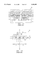
The general features of a pair of prior art DRAM cells generally designated as 10 are shown as a cross-sectional view in FIG. 1A. DRAM cells 10 have a substrate 12 that is formed having a conductivity type which is one of either a P-type conductivity or a N-type conductivity, if the substrate 12 is silicon based. Substrate 12 may be made of silicon, gallium arsenide, silicon on insulator (SOI) structures, epitaxial formations, germanium, germanium silicon, polysilicon, amorphous silicon, and/or like substrate, semi-conductive or conductive. The substrate 12 is typically made of single crystal silicon, and is usually lightly doped with boron, phosphorous or arsenic atoms.
A moat or active area region 14 is shown disposed within a field oxide region 16 which has been grown from substrate 12 if the substrate 12 is silicon based. The moat region 14, generally formed by diffusion, has disposed therein conductive source/drain regions 20. The common source/drain 18 (common to both cells), located within moat 14, is connected to bitline contact 38 that is etched through an insulating layer 26.
Disposed adjacent to the conductive regions 20, and the common source/drain 18, are a gate oxides 28 and wordlines 30. Portions of the wordlines 30 also function as gates, which define the field effect transistors (FET) of the DRAM cells 10. The storage nodes 36 (lower plates of the capacitors) of the DRAM cells 10 are electrically connected to the conductive regions 20 by storage node contact 32. A storage node 36, dielectric layer 34 disposed over the storage node 36 and grounded upper plate 37 form the capacitor. The various components of the DRAM cell 10 are electrically isolated by insulating layers 26.
FIG. 1B is a top view of the design layout of a pair of prior art DRAM cells 10. Divided across centerline 39 are two 8f2 sized cells 11, 13 that define the DRAM cells 10. As best viewed in conjunction with FIG. 1A, a bitline contact 38 is disposed spanning one-half of one f unit across both 8f2 cells 11 and 13 of the DRAM cells 10. Bitline contact 38 is centrally located over the common source/drain 18. Located at a distance of one f unit on either side of bitline contact 38 are storage node contacts 32, which contact storage node 36 through conductive regions 20 to connect to the capacitor which is above the wordlines 30 and the storage node contacts 32. Wordlines 30 have a width of one f unit, which is generally the same as the diameter of the storage node contacts 32. Perpendicular to the wordlines 30 is a bitline 22 that is depicted atop the units 11 and 13 and which forms an electrical contact with bitline contact 38. Bitline 22 also has a width of one f unit and is longitudinally centered over the DRAM unit cell 10.
FIG. 1C shows a simplified layout of four pair DRAM unit cells 10 of the prior art from a top view. The DRAM unit cells 10 in FIG. 1C are the same as the DRAM unit cells 10 in FIG. 13 and can be seen aligned as the wordlines 30 and bitlines 22 traverse multiple units. Following the standard rectangular 8f2 design rule along centerline 39, the positioning of bitline contacts 38 relative to each other and of storage node contacts 32 relative to each other, are best viewed in plan view. As is apparent from the top view, the bitline contacts 38 are disposed at a minimum distance of three to three and a half f units when measured horizontally, vertically, or diagonally. The top view highlights the large gaps that exist between storage node contacts 22, for example, a distance of up to three f units. These large distances between bitline contacts 38 and storage node contacts 32 (collectively, self aligning contacts (SAC)), cause large problems during photolithography because dark areas are difficult to achieve when using Levenson Phaseshift.
Large distances between bitline contacts and storage node contacts cause large problems during photolithography because dark areas are difficult to achieve when using Levenson Phaseshift. Because Levenson Phaseshift depends on wave cancellations between nearby features, commonly known as destructive interferences, the resultant printability of the pattern is largely a function of the symmetry and separation distances. When non-symmetries in the pattern occur, the result is weaker cancellations of fields (i.e. between features) and a large loss of image contrast and depth of focus during the printing step. The net result are defects, which increase device failure, which can be significantly reduced by the geometry modifications disclosed herein.
The present invention generally follows the design rule for cell design and isolation following the typical design rules for cells, such as, 8f2 -based cells. The present invention also generally follows the design and processing rules when viewing the cell in a cross-sectional manner. The present invention, however, departs from conventional cell design in order to achieve the improvements necessary to reduce the design rule and wiring design patterns for use with current lithographic equipment. Lithographic machines having a light source with a wavelength of, for example, 248 nanometers for a KrF laser can be used to create the design patterns required for cells using an f value of 0.16 or 0.13 micrometers. This is only true, however, for strong phase shift under "ideal" conditions.
Using the present invention, cells having a design pattern of 0.16 μm to 0.13 μm can be achieved taking advantage of the Levenson Phaseshift Technique. The Levenson Phaseshift Technique, as is known to those in the art, can be used to produce design patterns smaller than those of the wavelength of the light source by taking advantage of the wave-like characteristics of light. In the cell described herein, an ideal and natural symmetry is employed in the phase shift application. This symmetry, the hexagonal structure, leads to a uniquely balanced interaction between geometries. Because of this balance, the result is an image that is produced with improved contrast and depth of focus. Ultimately, this leads to less defects and improved yields of the circuit.
Turning now to a DRAM embodiment of the present invention, a portion of the mask design for use with the present invention is shown in FIG. 2A having bitline contacts 38 and storage node contacts 32 shown in a hexagonally symmetric pattern. The DRAM (two-cell) unit 100 is depicted from a top view as containing a bitline contact 38 and two storage node contacts 32 in alignment with adjacent DRAM units 100.
Turning to FIG. 2B, the dimensions and symmetry of the DRAM unit 100 (where a unit is a pair of cells) is described in more detail. As is shown by a closeup top view of the hexagonal symmetry, the area dimensions of the DRAM unit 100 can be made to match the standard 8f2 per cell design rule area. The storage node contacts 32 form a hexagonal arrangement around the bitline contacts 38. To obtain the values for the length and width of the DRAM unit 100, the value h is used to define the distance between the center of the nearest storage node contact 32 or bitline contact 38, collectively referred to herein as self-aligning contacts, to obtain the distance necessary to achieve isolation for design pattern geometries of 0.16 and 0.13 micrometers. The term "self-aligned contacts" as used herein is used to describe both bitline contacts 38 and storage node contacts 32, and are "aligned" because their position is defined by a single exposure of a single mask, thereby, eliminating the misalignment that occurs between masking operations.
Because the DRAM unit 100 is hexagonally symmetric, the dimensions of the DRAM unit 100 can be calculated based on the internal 60 degree angles of a hexagon. Based on a center-to-center distance labeled h, one obtains a value of h divided by 2 for the diameter of each self-aligned contact, again, based on standard 8f2 geometry. Therefore, the individual transistor units 11 and 13 can be defined as having a length that is 3/2 of h, and a width which is the square root of 3, divided 2, times h. The unit cell area for transistor 11 or transistor 13 is, therefore, the square root of 3, divided by 2, times h times 3/2 times h which gives us a cell size of 3/4 times the square root of 3 times h times h.
3/4√3×h×h=8f.sup.2
Using design rules for a design pattern having a value of f equal to 0.16 in the 8f2 model, and if we equate that to our transistor unit cell 11 or 13 area, we obtain h values for an f of 0.16 of h equals 0.40 micrometers. Turning to the f value of 0.13, we obtain a transistor unit cell 11 or 13 area of h equals 0.32 micrometers.
The self-aligned contact diameter, as explained hereinabove, is h/2 which gives a self-aligned contact diameter for the f value of 0.16 micrometer design lines of about 0.20 micrometers for the self-aligned contact. For the self-aligned contact having an f value of 0.13, the self-aligned contact diameter is about 0.16 micrometers.
SAC radius:
h/2=0.20 um for f=0.16 um
h/2=0.16 um for f=0.13 um
Based on these calculations, the area of the self-aligned contacts is actually larger than that of the typical design rule of 8f2.
The image realized on the silicon wafer is a Fourier transform of the mask image. In this simple arrangement, the high frequency part of the Fourier transform is smaller and, as a result, the image of the silicon wafer is closer to the image in a reticle, leading to an improvement in device patterning consistency, and therefore, to device performance. Improved consistency in patterning is achieved even when using the smaller design rules for f values of 0.16 and 0.13 micrometers.
Due to the hexagonal arrangement of the self-aligning contacts depicted in FIGS. 2A and 2B, in order for the wordlines 30 to contact the individual bitline contacts 38, instead of having straight wordlines as in the prior art, the wordline 30 of the present invention is designed so as to contact the bitline contacts 38, which are no longer aligned in a straight line.
Wordlines 30 are made as depicted in FIG. 3. In order to maintain the hexagonal symmetry of the DRAM unit 100, the wordline 30 has evenly spaced protrusions 50 that reach out to contact the bitline contact (not depicted) away from the centerline 39 of the wordline 30. In FIG. 3, the protrusions 50 of wordline 30 can be seen to face each other and form a wordline spacing 52 that provides isolation between the different wordlines 30.
In order to conform to the 8f2 design rule, we must solve for the values of the width of the wordline spacing 52 and for the size of the protrusions 50. As was seen in FIGS. 2A and 2B, we assume that the diameter of the bitline contact is h/2. Therefore, we calculate that the thickness of the wordline without protrusions 50 to be 3/10 of h. Again, based on the 8f2 assumption, we find that the wordline spacing 52 also has a width of 3/10 h. Returning to our design rule for the 8f2 pattern having a width of f equals 0.16, we solve for the f value and determine for f equals 0.16, that h has a value equal to about 0.119 micrometers. Likewise, for an f value of 0.13, the h value is about 0.097 micrometers.
The space 54 between protrusions 50 maintains the symmetry of the wordline spacing 52 and as described above, has a width of 3/10 h, again following the 8f2 design rule. The length of the protrusion 50, however, in a trapezoidal shape is resolved by the equation:
√3/2*h-3/10*h=area
giving us a width for the protrusion 50 based on a 0.16 geometry of about 0.225 micrometers in width. For the design geometry of f equals 0.13, the value for h is about 0.183 micrometers.
Bitline 22 to bitline 22 spacing is double that of the calculations made for the wordlines 30 and the wordline spacing 52, which gives us a length of 6/10ths of h, which for a 8f2 geometry of 0.16 equals to an h value of about 0.238 micrometers. Likewise, for the 8f2 geometry of 0.13, the value of h is about 0.194 micrometers.
FIG. 4 shows the design for moat region 14, which for use in this embodiment generally has a rectangular shape. The size of the rectangles can be defined according to the 8f2 design rule area. Therefore, we follow the central assumptions for the hexagonally symmetric DRAM unit 100 is that the geometries underlying the different components of the DRAM unit 100 will be assumed to equal that of the 8f2 design rule based on an f value of, for example, 0.16 and 0.13 micrometers.
√3/4*h=moatwidth/space
To calculate the space occupied by the moat region 14, one can calculate, for example, the width occupied by the width of the rectangular moat shape, which for an f value of 0.16 micrometers will yield a moat to width space area of about 0.17 micrometers. For an 8f2 design geometry of f=0.13 micrometers, the moat width per space will be about 0.14 micrometers.
Moat width/space:
=0.17 um for f=0.16 um
=0.14 um for f=0.13 um
As the length of the rectangle is 21/2 times the length h, we solve for the value of h, and for the value f having an f--equal to 0.16, yielding a moat region 14 length equal to about 3.993 micrometers. For an 8f2 geometry of 0.13, the h value for the length of the rectangular moat region 14 is about 0.807 micrometers. Likewise, the distance measured between the moat region rectangles as they are lined along their length can be calculated to be the square root of the value h. The region between adjacent rectangular lines 44 can be described as the square root of 3, divided by 4, of h. Finally, the distance between the center lines of the rectangular moat regions 14, designated herein as 46, is the square root of 3, divided by 2, of h, using h values as calculated above.
FIG. 5 shows the hexagonal arrangement 60 of the storage node contacts 32. The storage node contacts 32 form part of the self-aligning contacts and are depicted here in the hexagonal arrangement. The storage node contacts 32 and the bitline contacts 38, can be created using one or two masks. When used with Levenson Phaseshift, however, a one mask arrangement is preferred in order to maximize the area used and minimize dark areas.
FIG. 6 shows a top view of storage nodes 36, which also form a hexagonal shape around the bitline contacts 38. The storage node 36, while depicted as triangular in shape, may have alternative shapes, such as generally oval. The storage node contact 32 is shown as being centrally located within the outline of the storage node 36, however, alternative arrangements are possible.
As can be better viewed from the top view showing the storage node 36, in conjunction with the storage node contacts 32 and the bitline contacts 38, one can assume that the masking pattern for the storage node 36 is triangular. In order to obtain the surface area of the storage node 36, again based on the 8f2 design rule of geometry, and based on the hexagonal arrangement of the DRAM unit 100, one can assume that the distance between two bitlines contacts 38 is two times h. Based on this geometry, the distance between a bitline contact 38 and the closest edge of a storage node 36 is h divided by 4. As the distance between storage node contacts 38 is two times h, and the minimum distance between a bitline contact 38 and a storage node 36 is h/4, again from a top view, this permits us to have, an isosceles triangle having a per side length of (1 minus the square root of 2 divided by 4) times h.
To calculate the surface area of the surface node 36 based on the side length, we solve for h based on the following equation:
(6-3/2√3)ht+√3/4(1-√3/4).sup.2 h.sup.2
Using our 8f2 design rule assumption for surface size, and having a goal design pattern of f value equals 0.16, we obtain a surface area of about 0.359 micrometers for the surface area of the storage node 36. Likewise for the design geometry of f equals 0.13, we obtain a surface area of about 0.189 micrometers.
Based on a t value of 0.25 microns and a capacitance density of 76 femtoFarads (fF) per square micrometer, we obtain a capacitance density of 27 fF per cell for the design geometry having a value of f equals 0.16. Likewise for the f value of 0.13 micrometers, we obtain a capacitance density of 22 fF per cell. Using conventional 8f2 design rule, the capacitance density value obtained is 21 fF per cell for an f equals 0.16 micrometer geometry. Therefore, using the present invention increases the capacitance value of both the f equals 0.16 and f equals 0.13 design rule geometry.
Capacitance:
f=0.16; t=0.25 um=0.359 um2 =27 fF/cell
f=0.13; t=0.25 um=0.189 um2 =22 fF/cell
8f2 prior art storage node f=0.16=21 fF/cell
FIG. 7 shows the contour 70 of wordlines 30 that were made with a mask having square protrusions 50 extending from wordline 30. As can be seen in FIG. 9, the contour 70 on a silicon wafer provides sufficient distance between the alternating protrusions 50 of wordline 30 to provide electrical isolation between the bitline contacts. The contour 70 was created using a Krf laser having a wavelength of 248 mm.
FIG. 8 shows the hexagonal arrangement of the self aligned contacts, namely, storage node contacts 32 and bitline contacts 38 on a silicon wafer. As with FIG. 7, the pattern was created using a KrF laser having a wavelength of 248 nanometers. The self-aligning contact mask had square areas which form the generally oval contours depicted herein. As can be seen from the contours on the wafer surface, isolation of the self aligned contacts, namely, the storage node contacts 32 and bitline contacts 38 was achieved within the desired tolerances.
While this invention has been described in reference to illustrative embodiments, this description is not intended to be construed in a limiting sense. Various modifications and combinations of the illustrative embodiments, as well as other embodiments of the invention, will be apparent to persons skilled in the art upon reference to the description. It is therefore intended that the appended claims encompass any such modifications or embodiments.

Claims (17)

What is claimed is:
1. A DRAM circuit comprising:
a field effect transistor having a first source/drain and a second source/drain;
a bitline electrically connected to said first source/drain by a bitline contact;
at least six storage node contacts disposed hexagonally surrounding said bitline contact; and
at least six storage nodes electrically connected to said second source/drain by said at least six storage node contacts.
2. The DRAM circuit of claim 1, further comprising a wordline electrically connected to said field effect transistor, said wordline being disposed at an angle to said bitline.
3. The DRAM circuit of claim 2 wherein said wordline is further defined as comprising:
a centerline extending through said wordline; and
protrusions that extend from said centerline to form said transistor gate.
4. The DRAM circuit of claim 1 wherein said storage nodes are hexagonally arranged surrounding said bitline.
5. A DRAM circuit comprising:
a first source/drain;
a bitline electrically connected to said first source/drain by a bitline contact;
at least six storage node contacts disposed hexagonally surrounding said bitline contact;
at least six storage nodes electrically connected to a second source/drain by said at least six storage node contacts; and
a wordline electrically connected to a field effect transistor said wordline being disposed at an angle to said bitline;
the area covered by an individual DRAM cell being calculated by the formula (3/4) (31/2)×h×h=8f2, wherein said f is a design rule value and h is the closest distance between said storage node contacts and said bitline contact.
6. The DRAM circuit of claim 5 wherein the diameter of said bitline is h/2.
7. The DRAM circuit of claim 5 wherein the diameter of said storage node contact is h/2.
8. The DRAM circuit of claim 5 wherein said wordline is further defined as having protrusions with an area calculated by the formula:
√3/2*h-3/10*h=area
wherein h is the closest distance between said storage node contacts and said bitline contact.
9. The DRAM circuit of claim 5 wherein said storage node has an area defined by the following formula:
(6-3√3/2)ht+√3/4(1-√3/4).sup.2 h.sup.2
wherein h is the closest distance between said storage node contacts and said bitline contact, and t is the dielectric constant for said capacitor.
10. A hexagonally symmetric DRAM circuit on a silicon wafer comprising:
a pair of field effect transistors, each of said transistors having a common first source/drain and a separate gate;
a bitline contact in contact with said source/drain;
a bitline in electrical contact with said bitline contact;
six storage node contacts disposed surrounding said bitline contact; and
two wordlines, each said wordline providing a gate for one of said field effect transistors;
one or more storage nodes providing a portion of a capacitor with said storage node contacts.
11. The DRAM circuit of claim 10, wherein said storage nodes are hexagonally arranged surrounding said bitline.
12. The DRAM circuit of claim 10 wherein said wordline is further defined as comprising:
a centerline extending through said wordline; and
protrusions that extend from said centerline to form a gate transistor with said moat.
13. A hexagonally symmetric DRAM circuit on a silicon wafer comprising:
a first source/drain;
a bitline contact in contact with said source/drain;
a bitline in electrical contact with said bitline contact;
six storage node contacts disposed surrounding said bitline contact, and simultaneously formed with said bitline contact; and
two wordlines forming field effect transistor gates;
one or more storage nodes forming a capacitor with said storage node contacts;
an individual DRAM cell area being calculated by the formula: (3/4) (31/2)×h×h=8f2, wherein said f is a design rule value and h is the closest distance between said storage node contacts and said bitline contact.
14. The DRAM circuit of claim 13, wherein said storage node area is defined by the following formula:
(6-3√3/2)ht+√3/4(1-√3/4).sup.2 h.sub.2
wherein h is the closest distance between said storage node contacts and said bitline contact, and t is the dielectric constant for said capacitor.
15. The DRAM circuit of claim 13 wherein the diameter of said storage node contact is h/2.
16. A hexagonally symmetric DRAM circuit on a silicon wafer comprising:
a first source/drain;
a bitline contact in contact with said source/drain;
a bitline in electrical contact with said bitline contact;
six storage node contacts disposed surrounding said bitline contact, and simultaneously formed with said bitline contact; and
two wordlines forming field effect transistor gates;
one or more storage nodes forming a capacitor with said storage node contacts;
wherein the diameter of said bitline is h/2 wherein h is the closest distance between said storage node contacts and said bitline contact.
17. A hexagonally symmetric DRAM circuit on a silicon wafer comprising:
a first source/drain;
a bitline contact in contact with said source/drain;
a bitline in electrical contact with said bitline contact;
six storage node contacts disposed surrounding said bitline contact, and simultaneously formed with said bitline contact; and
two wordlines forming field effect transistor gates;
one or more storage nodes forming a capacitor with said storage node contacts;
a centerline extending through said wordline; and protrusions that extend from said centerline to form a transistor gate;
wherein said wordline is further defined as having protrusions with an area calculated by the formula /10*h=area wherein h is the closest distance between said storage node contacts and said bitline contact.
US09/216,251 1997-12-31 1998-12-18 Hexagonally symmetric integrated circuit cell Expired - Lifetime US6166408A (en)

Priority Applications (2)

Application Number Priority Date Filing Date Title
US09/216,251 US6166408A (en) 1997-12-31 1998-12-18 Hexagonally symmetric integrated circuit cell
US09/542,002 US6342420B1 (en) 1997-12-31 2000-04-03 Hexagonally symmetric integrated circuit cell

Applications Claiming Priority (2)

Application Number Priority Date Filing Date Title
US7029797P 1997-12-31 1997-12-31
US09/216,251 US6166408A (en) 1997-12-31 1998-12-18 Hexagonally symmetric integrated circuit cell

Related Child Applications (1)

Application Number Title Priority Date Filing Date
US09/542,002 Division US6342420B1 (en) 1997-12-31 2000-04-03 Hexagonally symmetric integrated circuit cell

Publications (1)

Publication Number Publication Date
US6166408A true US6166408A (en) 2000-12-26

Family

ID=26750997

Family Applications (2)

Application Number Title Priority Date Filing Date
US09/216,251 Expired - Lifetime US6166408A (en) 1997-12-31 1998-12-18 Hexagonally symmetric integrated circuit cell
US09/542,002 Expired - Lifetime US6342420B1 (en) 1997-12-31 2000-04-03 Hexagonally symmetric integrated circuit cell

Family Applications After (1)

Application Number Title Priority Date Filing Date
US09/542,002 Expired - Lifetime US6342420B1 (en) 1997-12-31 2000-04-03 Hexagonally symmetric integrated circuit cell

Country Status (1)

Country Link
US (2) US6166408A (en)

Cited By (3)

* Cited by examiner, † Cited by third party
Publication number Priority date Publication date Assignee Title
US6396096B1 (en) * 2000-06-21 2002-05-28 International Business Machines Corporation Design layout for a dense memory cell structure
US20050079386A1 (en) * 2003-10-01 2005-04-14 Board Of Regents, The University Of Texas System Compositions, methods and systems for making and using electronic paper
US20080297878A1 (en) * 2003-10-01 2008-12-04 Board Of Regents, The University Of Texas System Compositions, methods and systems for making and using electronic paper

Families Citing this family (3)

* Cited by examiner, † Cited by third party
Publication number Priority date Publication date Assignee Title
US6548347B2 (en) * 2001-04-12 2003-04-15 Micron Technology, Inc. Method of forming minimally spaced word lines
US7642572B2 (en) * 2007-04-13 2010-01-05 Qimonda Ag Integrated circuit having a memory cell array and method of forming an integrated circuit
KR102214506B1 (en) 2014-08-21 2021-02-09 삼성전자 주식회사 Semiconductor device having contact plugs and method for manufacturing the same

Citations (2)

* Cited by examiner, † Cited by third party
Publication number Priority date Publication date Assignee Title
US5789770A (en) * 1994-11-02 1998-08-04 Lsi Logic Corporation Hexagonal architecture with triangular shaped cells
US5998256A (en) * 1996-11-01 1999-12-07 Micron Technology, Inc. Semiconductor processing methods of forming devices on a substrate, forming device arrays on a substrate, forming conductive lines on a substrate, and forming capacitor arrays on a substrate, and integrated circuitry

Family Cites Families (1)

* Cited by examiner, † Cited by third party
Publication number Priority date Publication date Assignee Title
JP3368002B2 (en) * 1993-08-31 2003-01-20 三菱電機株式会社 Semiconductor storage device

Patent Citations (2)

* Cited by examiner, † Cited by third party
Publication number Priority date Publication date Assignee Title
US5789770A (en) * 1994-11-02 1998-08-04 Lsi Logic Corporation Hexagonal architecture with triangular shaped cells
US5998256A (en) * 1996-11-01 1999-12-07 Micron Technology, Inc. Semiconductor processing methods of forming devices on a substrate, forming device arrays on a substrate, forming conductive lines on a substrate, and forming capacitor arrays on a substrate, and integrated circuitry

Cited By (3)

* Cited by examiner, † Cited by third party
Publication number Priority date Publication date Assignee Title
US6396096B1 (en) * 2000-06-21 2002-05-28 International Business Machines Corporation Design layout for a dense memory cell structure
US20050079386A1 (en) * 2003-10-01 2005-04-14 Board Of Regents, The University Of Texas System Compositions, methods and systems for making and using electronic paper
US20080297878A1 (en) * 2003-10-01 2008-12-04 Board Of Regents, The University Of Texas System Compositions, methods and systems for making and using electronic paper

Also Published As

Publication number Publication date
US6342420B1 (en) 2002-01-29

Similar Documents

Publication Publication Date Title
KR100357297B1 (en) Ultra compact dram cell and method of making
KR100210629B1 (en) Semiconductor memory device
US7259065B2 (en) Method of forming trench in semiconductor device
US6166408A (en) Hexagonally symmetric integrated circuit cell
US6534803B2 (en) Electronic device, semiconductor device, and electrode forming method
US7022440B2 (en) Resist pattern defined by inwardly arched lines
KR20020076455A (en) Manufacturing method for semiconductor device
US6434732B2 (en) Semiconductor circuit design methods employing spacing constraints
KR0161438B1 (en) Semiconductor memory device and manufacture thereof
KR100341159B1 (en) Method of manufacturing semiconductor memory device using two etching patterns
US6249018B1 (en) Fabrication method to approach the conducting structure of a DRAM cell with straightforward bit line
US6468876B2 (en) Simple stack cell capacitor formation
JP3203776B2 (en) Method for manufacturing semiconductor device
JP3152195B2 (en) Method for producing conductor and electrode pattern
KR0135246B1 (en) Method of semiconductor memory
KR100486231B1 (en) Manufacturing method of capacitor having cylindric storage node structure for semiconductor device
KR100218295B1 (en) Semiconductor memory cell manufacturing method
KR100239704B1 (en) Method of fabricating a straight line type dram cell
KR960015527B1 (en) Semiconductor memory device
KR940009610B1 (en) Manufacturing method of highly integrated semiconductor memory device
KR920010194B1 (en) Contact for semicondcutor device and method for manufacturng of the same
KR950002033B1 (en) Semiconductor memory device and fabricating method thereof
KR970010683B1 (en) Semiconductor device & manufacturing method
KR100304284B1 (en) Contact formation method of semiconductor device
KR960003865B1 (en) Fabrication process of semiconductor device

Legal Events

Date Code Title Description
AS Assignment

Owner name: TEXAS INSTRUMENTS INCORPORATED, TEXAS

Free format text: ASSIGNMENT OF ASSIGNORS INTEREST;ASSIGNORS:NISHIMURA, AKITOSHI;OKUNO, YASUTOSHI;KHAMANKHAR, RAJESH;AND OTHERS;REEL/FRAME:009951/0711;SIGNING DATES FROM 19990323 TO 19990427

STCF Information on status: patent grant

Free format text: PATENTED CASE

AS Assignment

Owner name: MYKROLIS CORPORATION, MASSACHUSETTS

Free format text: ASSIGNMENT OF ASSIGNORS INTEREST;ASSIGNOR:MILLIPORE CORPORATION;REEL/FRAME:012134/0787

Effective date: 20010331

FPAY Fee payment

Year of fee payment: 4

FPAY Fee payment

Year of fee payment: 8

FPAY Fee payment

Year of fee payment: 12