US6163063A - Semiconductor device - Google Patents
Semiconductor device Download PDFInfo
- Publication number
- US6163063A US6163063A US09/557,502 US55750200A US6163063A US 6163063 A US6163063 A US 6163063A US 55750200 A US55750200 A US 55750200A US 6163063 A US6163063 A US 6163063A
- Authority
- US
- United States
- Prior art keywords
- pad
- semiconductor device
- external connection
- pads
- link
- Prior art date
- Legal status (The legal status is an assumption and is not a legal conclusion. Google has not performed a legal analysis and makes no representation as to the accuracy of the status listed.)
- Expired - Lifetime
Links
Images
Classifications
-
- H10P74/273—
-
- G—PHYSICS
- G01—MEASURING; TESTING
- G01R—MEASURING ELECTRIC VARIABLES; MEASURING MAGNETIC VARIABLES
- G01R31/00—Arrangements for testing electric properties; Arrangements for locating electric faults; Arrangements for electrical testing characterised by what is being tested not provided for elsewhere
- G01R31/28—Testing of electronic circuits, e.g. by signal tracer
- G01R31/2851—Testing of integrated circuits [IC]
- G01R31/2884—Testing of integrated circuits [IC] using dedicated test connectors, test elements or test circuits on the IC under test
Definitions
- the present invention relates, in general, to semiconductors, and more particularly, to a novel semiconductor device and method.
- Kelvin probing requires the placement of two probes on one electrical conductor in order to force a particular current and measure the voltage derived from such current.
- One problem with this technique is the large bonding pad area that is required to accommodate the Kelvin probes. Large bonding pads increase capacitance thereby degrading the performance of the RF transistor.
- bonding pads are required to be at least 100 microns in diameter in order to accommodate both Kelvin probes.
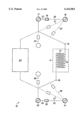
- FIGURE schematically illustrates a portion of a semiconductor device in accordance with the present invention.
- FIG. 1 schematically illustrates a semiconductor device 10 that minimizes the capacitance associated with the electrodes of device 10.
- Device 10 has an active area 11 that includes a first active element 12 and a second active element 13.
- Active element 12 could be the active elements of a transistor such as an emitter for a bipolar transistor or a source of a metal oxide semiconductor (MOS) transistor.
- Element 13 could be another active element of the transistor such as a base or a gate.
- Elements 12 and 13 are electrically connected to nodes or terminals, such as terminals 14 and 16, which facilitate electrically connecting elements 12 and 13 to circuits external to device 10.
- Device 10 is also formed to have a plurality of external connection pads such as a first external connection pad 17 and a second external connection pad 18.
- pads 17 and 18 are circular bonding pads of an RF transistor. As will be seen hereinafter, only pad 17 of this plurality of external connection pads is used to electrically connect device 10 to external circuits.
- Pads 17 and 18 are electrically connected together and also electrically connected to active elements, such as element 12 through terminal 14.
- Pad 18 is physically separated from pad 17 but is electrically connected to pad 17 through a first conductor 26, a second conductor 27, and an electrical link 19.
- First conductor 26 has one end connected to pad 18 and a second end connected to one end of link 19.
- second conductor 27 has a first end connected to link 19 and a second end connected to pad 17 to form the electrical connection between pads 17 and 18.
- Electrical link 19 typically is a fusible link such as a polysilicon fuse, a nichrome fuse, or other electrical link that can be used to electrically disconnect pad 17 from pad 18. Such electrical links are well known to those skilled in the semiconductor art. Activating link 19 typically involves supplying sufficient electrical current through link 19 to create an essentially open circuit. Link 19 is placed a sufficient distance from pad 17 to ensure that activating link 19 to remove the electrical connection between pads 17 and 18 does not disturb pad 17. Typically, link 19 is at least one hundred microns from pad 17. Pad 18 can be placed in a variety of locations and be electrically coupled through a variety of different paths as shown by dashed lines 21, 22, and 23. In the preferred embodiment, pad 18 is physically attached to pad 17. However in other embodiments, pad 18 may be physically attached to terminal 14 or other points along the conductor attached to element 12 but the accuracy of the measurements may be reduced.
- Active element 13 also has a plurality of external connection pads that function similarly to pads 17 and 18.
- a third external connection pad 32 and a fourth external connection pad 31 function similarly to pads 17 and 18, respectively.
- Pad 31 is electrically connected to pad 32 via a third conductor 33, a second electrical link 36, and a fourth conductor 34.
- Conductors 33 and 34 are similar to conductors 26 and 27, respectively, and link 36 is similar to link 19.
- Pad 32 is connected to a terminal 16 that is similar to terminal 14.
- Semiconductor device 10 may have a plurality of active areas that are similar to area 11 and connected to the external connection pads in parallel with area 11. Another such area is illustrated by a dashed box 24.
- Kelvin probing can be used to test device 10.
- One set of the Kelvin probe can have one probe placed on pad 17 and the second probe placed on pad 18.
- Another set of Kelvin probes can be placed on pads 31 and 32 thereby allowing testing of device 10.
- an electrical current is passed between pads 17 and 18 to remove the electrical coupling between pads 17 and 18.
- an electrical current is passed between pads 31 and 32 to remove the electrical coupling.
- the capacitance on pad 17 and thus on element 12 is reduced.
- the size of the pads can be smaller than the pads for a prior art transistor since only one Kelvin probe is placed on a pad.
- the capacitance on element 12 is one fourth the capacitance of a prior art transistor.
Landscapes
- Engineering & Computer Science (AREA)
- Computer Hardware Design (AREA)
- Microelectronics & Electronic Packaging (AREA)
- General Engineering & Computer Science (AREA)
- Physics & Mathematics (AREA)
- General Physics & Mathematics (AREA)
- Semiconductor Integrated Circuits (AREA)
- Testing Of Individual Semiconductor Devices (AREA)
- Testing Or Measuring Of Semiconductors Or The Like (AREA)
Abstract
Description
Claims (5)
Priority Applications (1)
| Application Number | Priority Date | Filing Date | Title |
|---|---|---|---|
| US09/557,502 US6163063A (en) | 1998-06-01 | 2000-04-24 | Semiconductor device |
Applications Claiming Priority (2)
| Application Number | Priority Date | Filing Date | Title |
|---|---|---|---|
| US09/088,019 US6140212A (en) | 1998-06-01 | 1998-06-01 | Semiconductor device and method therefor |
| US09/557,502 US6163063A (en) | 1998-06-01 | 2000-04-24 | Semiconductor device |
Related Parent Applications (1)
| Application Number | Title | Priority Date | Filing Date |
|---|---|---|---|
| US09/088,019 Division US6140212A (en) | 1998-06-01 | 1998-06-01 | Semiconductor device and method therefor |
Publications (1)
| Publication Number | Publication Date |
|---|---|
| US6163063A true US6163063A (en) | 2000-12-19 |
Family
ID=22208734
Family Applications (2)
| Application Number | Title | Priority Date | Filing Date |
|---|---|---|---|
| US09/088,019 Expired - Lifetime US6140212A (en) | 1998-06-01 | 1998-06-01 | Semiconductor device and method therefor |
| US09/557,502 Expired - Lifetime US6163063A (en) | 1998-06-01 | 2000-04-24 | Semiconductor device |
Family Applications Before (1)
| Application Number | Title | Priority Date | Filing Date |
|---|---|---|---|
| US09/088,019 Expired - Lifetime US6140212A (en) | 1998-06-01 | 1998-06-01 | Semiconductor device and method therefor |
Country Status (1)
| Country | Link |
|---|---|
| US (2) | US6140212A (en) |
Citations (7)
| Publication number | Priority date | Publication date | Assignee | Title |
|---|---|---|---|---|
| US4933898A (en) * | 1989-01-12 | 1990-06-12 | General Instrument Corporation | Secure integrated circuit chip with conductive shield |
| US5331195A (en) * | 1991-06-21 | 1994-07-19 | Nippon Steel Corporation | Fuse construction of a semiconductor device |
| US5382831A (en) * | 1992-12-14 | 1995-01-17 | Digital Equipment Corporation | Integrated circuit metal film interconnect having enhanced resistance to electromigration |
| US5410163A (en) * | 1992-03-18 | 1995-04-25 | Fujitsu Limited | Semi-conductor integrated circuit device including connection and disconnection mechanisms to connect and disconnect monitor circuit and semiconductor integrated circuit from each other |
| US5530277A (en) * | 1993-10-14 | 1996-06-25 | Fuji Electric Co., Ltd. | Insulated-gate bipolar transistor |
| US5710538A (en) * | 1995-09-27 | 1998-01-20 | Micrel, Inc. | Circuit having trim pads formed in scribe channel |
| US5780921A (en) * | 1995-08-30 | 1998-07-14 | Nec Corporation | Bipolar transistor constant voltage source circuit |
-
1998
- 1998-06-01 US US09/088,019 patent/US6140212A/en not_active Expired - Lifetime
-
2000
- 2000-04-24 US US09/557,502 patent/US6163063A/en not_active Expired - Lifetime
Patent Citations (7)
| Publication number | Priority date | Publication date | Assignee | Title |
|---|---|---|---|---|
| US4933898A (en) * | 1989-01-12 | 1990-06-12 | General Instrument Corporation | Secure integrated circuit chip with conductive shield |
| US5331195A (en) * | 1991-06-21 | 1994-07-19 | Nippon Steel Corporation | Fuse construction of a semiconductor device |
| US5410163A (en) * | 1992-03-18 | 1995-04-25 | Fujitsu Limited | Semi-conductor integrated circuit device including connection and disconnection mechanisms to connect and disconnect monitor circuit and semiconductor integrated circuit from each other |
| US5382831A (en) * | 1992-12-14 | 1995-01-17 | Digital Equipment Corporation | Integrated circuit metal film interconnect having enhanced resistance to electromigration |
| US5530277A (en) * | 1993-10-14 | 1996-06-25 | Fuji Electric Co., Ltd. | Insulated-gate bipolar transistor |
| US5780921A (en) * | 1995-08-30 | 1998-07-14 | Nec Corporation | Bipolar transistor constant voltage source circuit |
| US5710538A (en) * | 1995-09-27 | 1998-01-20 | Micrel, Inc. | Circuit having trim pads formed in scribe channel |
Also Published As
| Publication number | Publication date |
|---|---|
| US6140212A (en) | 2000-10-31 |
Similar Documents
| Publication | Publication Date | Title |
|---|---|---|
| US5444366A (en) | Wafer burn-in and test system | |
| US6383825B1 (en) | Method and system for testing semiconductor dice, semiconductor packages and semiconductor wafers | |
| KR980005984A (en) | Test Methods for Multiple Integrated Circuits on Semiconductor Wafers | |
| US5381105A (en) | Method of testing a semiconductor device having a first circuit electrically isolated from a second circuit | |
| EP0720023B1 (en) | Test method for power integrated devices | |
| US5897193A (en) | Semiconductor wafer | |
| JPH05267415A (en) | Semiconductor device | |
| US6163063A (en) | Semiconductor device | |
| US6911357B2 (en) | Method for wafer level testing of semiconductor using sacrificial on die power and ground metalization | |
| JP2657315B2 (en) | Probe card | |
| JP3495835B2 (en) | Semiconductor integrated circuit device and inspection method thereof | |
| US6809378B2 (en) | Structure for temporarily isolating a die from a common conductor to facilitate wafer level testing | |
| KR100396344B1 (en) | Monitoring resistor element and measuring method of relative preciseness of resistor elements | |
| JPH10233419A (en) | Semiconductor device | |
| JP2634286B2 (en) | Handler device for testing electrical characteristics of semiconductor devices | |
| JP2002280428A (en) | Method for manufacturing semiconductor device | |
| KR100352113B1 (en) | calibration kit for testing a transistor | |
| JPH0566732B2 (en) | ||
| KR0151836B1 (en) | Wafer level burn-in and its method | |
| US20080122446A1 (en) | Test pattern | |
| JPH1073634A (en) | Ic socket and test method of ic using the ic socket | |
| JP3324770B2 (en) | Semiconductor wafer for burn-in and test of semiconductor devices | |
| JP2978883B1 (en) | Semiconductor device | |
| JP2001217390A (en) | High integrated circuit chip having element to be evaluated, and method of inspecting the element | |
| Schwartz | Electrical Testing in Failure Analysis-The Role of the Curve Tracer |
Legal Events
| Date | Code | Title | Description |
|---|---|---|---|
| STCF | Information on status: patent grant |
Free format text: PATENTED CASE |
|
| AS | Assignment |
Owner name: FREESCALE SEMICONDUCTOR, INC., TEXAS Free format text: ASSIGNMENT OF ASSIGNORS INTEREST;ASSIGNOR:MOTOROLA, INC.;REEL/FRAME:015698/0657 Effective date: 20040404 Owner name: FREESCALE SEMICONDUCTOR, INC.,TEXAS Free format text: ASSIGNMENT OF ASSIGNORS INTEREST;ASSIGNOR:MOTOROLA, INC.;REEL/FRAME:015698/0657 Effective date: 20040404 |
|
| FPAY | Fee payment |
Year of fee payment: 4 |
|
| AS | Assignment |
Owner name: CITIBANK, N.A. AS COLLATERAL AGENT, NEW YORK Free format text: SECURITY AGREEMENT;ASSIGNORS:FREESCALE SEMICONDUCTOR, INC.;FREESCALE ACQUISITION CORPORATION;FREESCALE ACQUISITION HOLDINGS CORP.;AND OTHERS;REEL/FRAME:018855/0129 Effective date: 20061201 Owner name: CITIBANK, N.A. AS COLLATERAL AGENT,NEW YORK Free format text: SECURITY AGREEMENT;ASSIGNORS:FREESCALE SEMICONDUCTOR, INC.;FREESCALE ACQUISITION CORPORATION;FREESCALE ACQUISITION HOLDINGS CORP.;AND OTHERS;REEL/FRAME:018855/0129 Effective date: 20061201 |
|
| FPAY | Fee payment |
Year of fee payment: 8 |
|
| AS | Assignment |
Owner name: CITIBANK, N.A., AS COLLATERAL AGENT,NEW YORK Free format text: SECURITY AGREEMENT;ASSIGNOR:FREESCALE SEMICONDUCTOR, INC.;REEL/FRAME:024397/0001 Effective date: 20100413 Owner name: CITIBANK, N.A., AS COLLATERAL AGENT, NEW YORK Free format text: SECURITY AGREEMENT;ASSIGNOR:FREESCALE SEMICONDUCTOR, INC.;REEL/FRAME:024397/0001 Effective date: 20100413 |
|
| FPAY | Fee payment |
Year of fee payment: 12 |
|
| AS | Assignment |
Owner name: CITIBANK, N.A., AS NOTES COLLATERAL AGENT, NEW YORK Free format text: SECURITY AGREEMENT;ASSIGNOR:FREESCALE SEMICONDUCTOR, INC.;REEL/FRAME:030633/0424 Effective date: 20130521 Owner name: CITIBANK, N.A., AS NOTES COLLATERAL AGENT, NEW YOR Free format text: SECURITY AGREEMENT;ASSIGNOR:FREESCALE SEMICONDUCTOR, INC.;REEL/FRAME:030633/0424 Effective date: 20130521 |
|
| AS | Assignment |
Owner name: CITIBANK, N.A., AS NOTES COLLATERAL AGENT, NEW YORK Free format text: SECURITY AGREEMENT;ASSIGNOR:FREESCALE SEMICONDUCTOR, INC.;REEL/FRAME:031591/0266 Effective date: 20131101 Owner name: CITIBANK, N.A., AS NOTES COLLATERAL AGENT, NEW YOR Free format text: SECURITY AGREEMENT;ASSIGNOR:FREESCALE SEMICONDUCTOR, INC.;REEL/FRAME:031591/0266 Effective date: 20131101 |
|
| AS | Assignment |
Owner name: FREESCALE SEMICONDUCTOR, INC., TEXAS Free format text: PATENT RELEASE;ASSIGNOR:CITIBANK, N.A., AS COLLATERAL AGENT;REEL/FRAME:037354/0225 Effective date: 20151207 Owner name: FREESCALE SEMICONDUCTOR, INC., TEXAS Free format text: PATENT RELEASE;ASSIGNOR:CITIBANK, N.A., AS COLLATERAL AGENT;REEL/FRAME:037356/0143 Effective date: 20151207 Owner name: FREESCALE SEMICONDUCTOR, INC., TEXAS Free format text: PATENT RELEASE;ASSIGNOR:CITIBANK, N.A., AS COLLATERAL AGENT;REEL/FRAME:037356/0553 Effective date: 20151207 |
|
| AS | Assignment |
Owner name: MORGAN STANLEY SENIOR FUNDING, INC., MARYLAND Free format text: ASSIGNMENT AND ASSUMPTION OF SECURITY INTEREST IN PATENTS;ASSIGNOR:CITIBANK, N.A.;REEL/FRAME:037486/0517 Effective date: 20151207 |
|
| AS | Assignment |
Owner name: MORGAN STANLEY SENIOR FUNDING, INC., MARYLAND Free format text: ASSIGNMENT AND ASSUMPTION OF SECURITY INTEREST IN PATENTS;ASSIGNOR:CITIBANK, N.A.;REEL/FRAME:037518/0292 Effective date: 20151207 |
|
| AS | Assignment |
Owner name: MORGAN STANLEY SENIOR FUNDING, INC., MARYLAND Free format text: SUPPLEMENT TO THE SECURITY AGREEMENT;ASSIGNOR:FREESCALE SEMICONDUCTOR, INC.;REEL/FRAME:039138/0001 Effective date: 20160525 |
|
| AS | Assignment |
Owner name: NXP, B.V., F/K/A FREESCALE SEMICONDUCTOR, INC., NETHERLANDS Free format text: RELEASE BY SECURED PARTY;ASSIGNOR:MORGAN STANLEY SENIOR FUNDING, INC.;REEL/FRAME:040925/0001 Effective date: 20160912 Owner name: NXP, B.V., F/K/A FREESCALE SEMICONDUCTOR, INC., NE Free format text: RELEASE BY SECURED PARTY;ASSIGNOR:MORGAN STANLEY SENIOR FUNDING, INC.;REEL/FRAME:040925/0001 Effective date: 20160912 |
|
| AS | Assignment |
Owner name: NXP B.V., NETHERLANDS Free format text: RELEASE BY SECURED PARTY;ASSIGNOR:MORGAN STANLEY SENIOR FUNDING, INC.;REEL/FRAME:040928/0001 Effective date: 20160622 |
|
| AS | Assignment |
Owner name: NXP USA, INC., TEXAS Free format text: CHANGE OF NAME;ASSIGNOR:FREESCALE SEMICONDUCTOR, INC.;REEL/FRAME:040652/0241 Effective date: 20161107 Owner name: NXP USA, INC., TEXAS Free format text: MERGER;ASSIGNOR:FREESCALE SEMICONDUCTOR, INC.;REEL/FRAME:040652/0241 Effective date: 20161107 |
|
| AS | Assignment |
Owner name: NXP USA, INC., TEXAS Free format text: CORRECTIVE ASSIGNMENT TO CORRECT THE NATURE OF CONVEYANCE PREVIOUSLY RECORDED AT REEL: 040652 FRAME: 0241. ASSIGNOR(S) HEREBY CONFIRMS THE MERGER AND CHANGE OF NAME;ASSIGNOR:FREESCALE SEMICONDUCTOR, INC.;REEL/FRAME:041260/0850 Effective date: 20161107 |
|
| AS | Assignment |
Owner name: MORGAN STANLEY SENIOR FUNDING, INC., MARYLAND Free format text: CORRECTIVE ASSIGNMENT TO CORRECT THE REMOVE PATENTS 8108266 AND 8062324 AND REPLACE THEM WITH 6108266 AND 8060324 PREVIOUSLY RECORDED ON REEL 037518 FRAME 0292. ASSIGNOR(S) HEREBY CONFIRMS THE ASSIGNMENT AND ASSUMPTION OF SECURITY INTEREST IN PATENTS;ASSIGNOR:CITIBANK, N.A.;REEL/FRAME:041703/0536 Effective date: 20151207 |
|
| AS | Assignment |
Owner name: SHENZHEN XINGUODU TECHNOLOGY CO., LTD., CHINA Free format text: CORRECTIVE ASSIGNMENT TO CORRECT THE TO CORRECT THE APPLICATION NO. FROM 13,883,290 TO 13,833,290 PREVIOUSLY RECORDED ON REEL 041703 FRAME 0536. ASSIGNOR(S) HEREBY CONFIRMS THE THE ASSIGNMENT AND ASSUMPTION OF SECURITYINTEREST IN PATENTS.;ASSIGNOR:MORGAN STANLEY SENIOR FUNDING, INC.;REEL/FRAME:048734/0001 Effective date: 20190217 Owner name: SHENZHEN XINGUODU TECHNOLOGY CO., LTD., CHINA Free format text: CORRECTIVE ASSIGNMENT TO CORRECT THE TO CORRECT THE APPLICATION NO. FROM 13,883,290 TO 13,833,290 PREVIOUSLY RECORDED ON REEL 041703 FRAME 0536. ASSIGNOR(S) HEREBY CONFIRMS THE THE ASSIGNMENT AND ASSUMPTION OF SECURITY INTEREST IN PATENTS.;ASSIGNOR:MORGAN STANLEY SENIOR FUNDING, INC.;REEL/FRAME:048734/0001 Effective date: 20190217 |
|
| AS | Assignment |
Owner name: NXP B.V., NETHERLANDS Free format text: RELEASE BY SECURED PARTY;ASSIGNOR:MORGAN STANLEY SENIOR FUNDING, INC.;REEL/FRAME:050744/0097 Effective date: 20190903 |
|
| AS | Assignment |
Owner name: MORGAN STANLEY SENIOR FUNDING, INC., MARYLAND Free format text: CORRECTIVE ASSIGNMENT TO CORRECT THE REMOVE APPLICATION11759915 AND REPLACE IT WITH APPLICATION 11759935 PREVIOUSLY RECORDED ON REEL 037486 FRAME 0517. ASSIGNOR(S) HEREBY CONFIRMS THE ASSIGNMENT AND ASSUMPTION OF SECURITYINTEREST IN PATENTS;ASSIGNOR:CITIBANK, N.A.;REEL/FRAME:053547/0421 Effective date: 20151207 Owner name: MORGAN STANLEY SENIOR FUNDING, INC., MARYLAND Free format text: CORRECTIVE ASSIGNMENT TO CORRECT THE REMOVE APPLICATION 11759915 AND REPLACE IT WITH APPLICATION 11759935 PREVIOUSLY RECORDED ON REEL 037486 FRAME 0517. ASSIGNOR(S) HEREBY CONFIRMS THE ASSIGNMENT AND ASSUMPTION OF SECURITY INTEREST IN PATENTS;ASSIGNOR:CITIBANK, N.A.;REEL/FRAME:053547/0421 Effective date: 20151207 |
|
| AS | Assignment |
Owner name: NXP B.V., NETHERLANDS Free format text: CORRECTIVE ASSIGNMENT TO CORRECT THE REMOVEAPPLICATION 11759915 AND REPLACE IT WITH APPLICATION11759935 PREVIOUSLY RECORDED ON REEL 040928 FRAME 0001. ASSIGNOR(S) HEREBY CONFIRMS THE RELEASE OF SECURITYINTEREST;ASSIGNOR:MORGAN STANLEY SENIOR FUNDING, INC.;REEL/FRAME:052915/0001 Effective date: 20160622 Owner name: NXP B.V., NETHERLANDS Free format text: CORRECTIVE ASSIGNMENT TO CORRECT THE REMOVE APPLICATION 11759915 AND REPLACE IT WITH APPLICATION 11759935 PREVIOUSLY RECORDED ON REEL 040928 FRAME 0001. ASSIGNOR(S) HEREBY CONFIRMS THE RELEASE OF SECURITY INTEREST;ASSIGNOR:MORGAN STANLEY SENIOR FUNDING, INC.;REEL/FRAME:052915/0001 Effective date: 20160622 |
|
| AS | Assignment |
Owner name: NXP, B.V. F/K/A FREESCALE SEMICONDUCTOR, INC., NETHERLANDS Free format text: CORRECTIVE ASSIGNMENT TO CORRECT THE REMOVEAPPLICATION 11759915 AND REPLACE IT WITH APPLICATION11759935 PREVIOUSLY RECORDED ON REEL 040925 FRAME 0001. ASSIGNOR(S) HEREBY CONFIRMS THE RELEASE OF SECURITYINTEREST;ASSIGNOR:MORGAN STANLEY SENIOR FUNDING, INC.;REEL/FRAME:052917/0001 Effective date: 20160912 Owner name: NXP, B.V. F/K/A FREESCALE SEMICONDUCTOR, INC., NETHERLANDS Free format text: CORRECTIVE ASSIGNMENT TO CORRECT THE REMOVE APPLICATION 11759915 AND REPLACE IT WITH APPLICATION 11759935 PREVIOUSLY RECORDED ON REEL 040925 FRAME 0001. ASSIGNOR(S) HEREBY CONFIRMS THE RELEASE OF SECURITY INTEREST;ASSIGNOR:MORGAN STANLEY SENIOR FUNDING, INC.;REEL/FRAME:052917/0001 Effective date: 20160912 |