US6150967A - Semiconductor integrated circuit - Google Patents
Semiconductor integrated circuit Download PDFInfo
- Publication number
- US6150967A US6150967A US09/229,995 US22999599A US6150967A US 6150967 A US6150967 A US 6150967A US 22999599 A US22999599 A US 22999599A US 6150967 A US6150967 A US 6150967A
- Authority
- US
- United States
- Prior art keywords
- current
- circuit
- output
- output sensor
- input
- Prior art date
- Legal status (The legal status is an assumption and is not a legal conclusion. Google has not performed a legal analysis and makes no representation as to the accuracy of the status listed.)
- Expired - Fee Related
Links
- 239000004065 semiconductor Substances 0.000 title claims description 15
- 238000006243 chemical reaction Methods 0.000 claims abstract description 9
- 239000000758 substrate Substances 0.000 claims description 5
- 238000010586 diagram Methods 0.000 description 7
- 238000000034 method Methods 0.000 description 2
- 230000006835 compression Effects 0.000 description 1
- 238000007906 compression Methods 0.000 description 1
- 239000011159 matrix material Substances 0.000 description 1
- 238000005070 sampling Methods 0.000 description 1
Images


Classifications
-
- H—ELECTRICITY
- H03—ELECTRONIC CIRCUITRY
- H03M—CODING; DECODING; CODE CONVERSION IN GENERAL
- H03M1/00—Analogue/digital conversion; Digital/analogue conversion
- H03M1/12—Analogue/digital converters
- H03M1/124—Sampling or signal conditioning arrangements specially adapted for A/D converters
- H03M1/1245—Details of sampling arrangements or methods
- H03M1/125—Asynchronous, i.e. free-running operation within each conversion cycle
-
- G—PHYSICS
- G01—MEASURING; TESTING
- G01R—MEASURING ELECTRIC VARIABLES; MEASURING MAGNETIC VARIABLES
- G01R19/00—Arrangements for measuring currents or voltages or for indicating presence or sign thereof
- G01R19/25—Arrangements for measuring currents or voltages or for indicating presence or sign thereof using digital measurement techniques
- G01R19/2506—Arrangements for conditioning or analysing measured signals, e.g. for indicating peak values ; Details concerning sampling, digitizing or waveform capturing
- G01R19/2509—Details concerning sampling, digitizing or waveform capturing
-
- H—ELECTRICITY
- H03—ELECTRONIC CIRCUITRY
- H03M—CODING; DECODING; CODE CONVERSION IN GENERAL
- H03M1/00—Analogue/digital conversion; Digital/analogue conversion
- H03M1/12—Analogue/digital converters
- H03M1/34—Analogue value compared with reference values
- H03M1/38—Analogue value compared with reference values sequentially only, e.g. successive approximation type
- H03M1/44—Sequential comparisons in series-connected stages with change in value of analogue signal
- H03M1/447—Sequential comparisons in series-connected stages with change in value of analogue signal using current mode circuits, i.e. circuits in which the information is represented by current values rather than by voltage values
Definitions
- the present invention relates to a semiconductor integrated circuit and, more particularly, to a semiconductor integrated circuit having a current output sensor and a means for processing an output signal from the current output sensor.
- An output signal from a current output sensor is conventionally processed by a circuit having an arrangement shown in FIG. 1.
- the current output sensor is a photodiode.
- a current output from a photodiode 1 must have a dynamic range of about 80 dB or more from a dark state to a bright state.
- this current signal is processed by, e.g., a 5-V single power source, the signal is first logarithmically compressed by an operational amplifier 23 and a diode 33.
- An output V O1 from the operational amplifier 23 is ##EQU1## where V c is the reference voltage, I S1 is the reverse saturation current of the photodiode, and I OP is the output current from the photodiode.
- the output V O1 is changed into an output V O2 by a transistor 43 for compensating a dark current.
- the output V O2 is ##EQU2## where I B is the value of a constant current 53, and I S2 is the reverse saturation current of the transistor 43.
- a buffer 63 changes the impedance.
- An operational amplifier 93 adjusts a signal to an input range for an AD (analog-to-digital) converter in cooperation with resistors 73 and 83.
- An output V O from the operational amplifier 93 is ##EQU5## where R 1 is the value of the resistor 73, and R 2 is the value of the resistor 83. This output V O is A/D-converted and then transmitted to a CPU or the like.
- the present invention has been made in consideration of the above situation, and has as its object to process an output from a current output sensor with a smaller number of elements (simple circuit arrangement).
- a semiconductor integrated circuit comprising a current output sensor, and current AD conversion means connected to an output side of the current output sensor to connect an output from the current output sensor to an input side of a comparator via a current mirror circuit and A/D (analog-to-digital)-convert the output from the current output sensor.
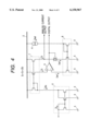
- FIG. 1 is a schematic circuit diagram showing an example of a signal processing circuit using a current output sensor
- FIG. 2 is a schematic block diagram for explaining an example of a semiconductor integrated circuit according to the present invention.
- FIG. 3 is a schematic block diagram for explaining an example of an AD converter according to the present invention.
- FIG. 4 is a schematic circuit diagram for explaining the example of the AD converter.
- FIGS. 5 and 6 are schematic layout views for explaining examples of the layout of functional elements on a semiconductor substrate.
- FIG. 2 is a block diagram showing a semiconductor integrated circuit according to an embodiment of the present invention.
- the semiconductor integrated circuit comprises a current output sensor 1 such as a photodiode or phototransistor (in this embodiment, a photodiode), a power source 2, 1-bit current input AD converters 3, and a constant current source 4 for generating a reference current.
- a current output sensor 1 such as a photodiode or phototransistor (in this embodiment, a photodiode)
- a power source 2 1-bit current input AD converters 3
- a constant current source 4 for generating a reference current.
- FIG. 3 is a schematic block diagram showing an example of each 1-bit current input AD converter 3 in FIG. 2.
- the 1-bit current input AD converter 3 is constituted by an N-type current mirror circuit 6 for receiving an input signal current, a P-type current mirror circuit 7 for receiving an output from the N-type current mirror circuit 6, an N-type current mirror circuit 8 connected to the constant current source 4 to generate a comparison reference current for each 1-bit current input AD converter 3, a current comparator 9 for comparing an output from the P-type current mirror circuit 7 with an output from the N-type current mirror circuit 8 for generating a comparison reference current, and an analog switch 10 controlled by an output from the current comparator 9.
- FIG. 4 is a circuit diagram showing an example of the detailed arrangement of the circuit in FIG. 3.
- n 1-bit current input AD converters set to the same reference current are series-connected, and sequentially perform the above operation while doubling a current input to each 1-bit AD converter.
- the same result can also be obtained by reducing the reference current to 1/2 from an MSB (Most Significant Bit) without doubling the input current by the P-type current mirror circuit 7.
- MSB Mobile Bit
- the integrated circuit is more advantageous in doubling the input current by the P-type current mirror circuit 7 because the same cell can be used.
- the reference current is reduced to 1/2, only one transistor is arranged on the output side of the N-type current mirror circuit 6. The N and P types of the current mirror circuits can be reversed.
- FIG. 5 is a schematic view showing an example of the layout in which one sensor (photodiode) and n-bit current input AD converters are formed on the same semiconductor substrate.
- FIG. 6 is a schematic view showing an example of the layout in which a photo area sensor (constituted by arranging photodiodes in a matrix), a timing control circuit, a current sampling/holding (S/H) circuit, and n-bit current input AD converters are formed on the same semiconductor substrate.
- a photo area sensor constituted by arranging photodiodes in a matrix
- S/H current sampling/holding
- an output current from the current output sensor is directly connected to the current AD conversion means, which can simplify the circuit arrangement and can decrease the number of elements and the power consumption.
- the current output sensor can be directly series-connected to n 1-bit current input AD converters to obtain an n-bit digital output, thereby greatly reducing the number of elements, the power consumption, the chip size, and the cost.
- a simple current input AD converter can be realized to facilitate the chip design and decrease the power consumption.
Abstract
Description
Claims (9)
Priority Applications (1)
| Application Number | Priority Date | Filing Date | Title |
|---|---|---|---|
| US09/662,605 US6392582B1 (en) | 1998-01-21 | 2000-09-14 | Semiconductor integrated circuit |
Applications Claiming Priority (2)
| Application Number | Priority Date | Filing Date | Title |
|---|---|---|---|
| JP10009429A JPH11214998A (en) | 1998-01-21 | 1998-01-21 | Semiconductor integrated circuit |
| JP10-009429 | 1998-01-21 |
Related Child Applications (1)
| Application Number | Title | Priority Date | Filing Date |
|---|---|---|---|
| US09/662,605 Division US6392582B1 (en) | 1998-01-21 | 2000-09-14 | Semiconductor integrated circuit |
Publications (1)
| Publication Number | Publication Date |
|---|---|
| US6150967A true US6150967A (en) | 2000-11-21 |
Family
ID=11720102
Family Applications (2)
| Application Number | Title | Priority Date | Filing Date |
|---|---|---|---|
| US09/229,995 Expired - Fee Related US6150967A (en) | 1998-01-21 | 1999-01-14 | Semiconductor integrated circuit |
| US09/662,605 Expired - Fee Related US6392582B1 (en) | 1998-01-21 | 2000-09-14 | Semiconductor integrated circuit |
Family Applications After (1)
| Application Number | Title | Priority Date | Filing Date |
|---|---|---|---|
| US09/662,605 Expired - Fee Related US6392582B1 (en) | 1998-01-21 | 2000-09-14 | Semiconductor integrated circuit |
Country Status (3)
| Country | Link |
|---|---|
| US (2) | US6150967A (en) |
| EP (1) | EP0932047A1 (en) |
| JP (1) | JPH11214998A (en) |
Cited By (12)
| Publication number | Priority date | Publication date | Assignee | Title |
|---|---|---|---|---|
| US6392582B1 (en) * | 1998-01-21 | 2002-05-21 | Canon Kabushiki Kaisha | Semiconductor integrated circuit |
| US6762706B2 (en) * | 2002-06-12 | 2004-07-13 | Freescale Semiconductor, Inc. | Reduced power analog-to-digital converter and method thereof |
| US20060158362A1 (en) * | 2003-10-21 | 2006-07-20 | Fujitsu Limited | D/A conversion circuit and A/D conversion circuit |
| US20070252829A1 (en) * | 2006-04-28 | 2007-11-01 | Epson Imaging Devices Corporation | Electronic circuit, electro-optical device, and electronic apparatus including the same |
| US20080024346A1 (en) * | 2006-07-25 | 2008-01-31 | Promax Technology (Hong Kong) Limited | Analog-to-digital conversion using asynchronous current-mode cyclic comparison |
| US20080048644A1 (en) * | 2006-07-26 | 2008-02-28 | Hales Rex K | Current Mode Analog-to-Digital Converter |
| US20190110012A1 (en) * | 2016-07-12 | 2019-04-11 | Olympus Corporation | Ad conversion circuit and imaging device |
| US10581448B1 (en) * | 2018-05-28 | 2020-03-03 | Ali Tasdighi Far | Thermometer current mode analog to digital converter |
| US10797718B1 (en) | 2018-04-17 | 2020-10-06 | Ali Tasdighi Far | Tiny low power current mode analog to digital converters for artificial intelligence |
| US10833692B1 (en) | 2018-04-17 | 2020-11-10 | Ali Tasdighi Far | Small low glitch current mode analog to digital converters for artificial intelligence |
| US10862495B1 (en) | 2018-04-17 | 2020-12-08 | Ali Tasdighi Far | Glitch free current mode analog to digital converters for artificial intelligence |
| DE102022202425A1 (en) | 2022-03-10 | 2023-09-14 | Robert Bosch Gesellschaft mit beschränkter Haftung | Device with a comparator device and method for operating a device with a comparator device |
Families Citing this family (6)
| Publication number | Priority date | Publication date | Assignee | Title |
|---|---|---|---|---|
| JP3681374B2 (en) | 2002-12-19 | 2005-08-10 | 株式会社日立製作所 | Current detection device and PWM inverter using the same |
| US7126509B2 (en) * | 2003-07-17 | 2006-10-24 | Massachusetts Institute Of Technology | Micropower logarithmic analog to digital conversion system and method with offset and temperature compensation |
| US6949968B1 (en) * | 2004-02-20 | 2005-09-27 | National Semiconductor Corporation | Method for increasing the sensitivity of integrated circuit temperature sensors |
| JP4137922B2 (en) * | 2005-06-23 | 2008-08-20 | 富士通株式会社 | A / D conversion circuit |
| US20090027821A1 (en) * | 2007-07-26 | 2009-01-29 | Littelfuse, Inc. | Integrated thermistor and metallic element device and method |
| US7659840B2 (en) * | 2008-02-15 | 2010-02-09 | Analog Devices, Inc. | Sigma-delta conversion circuit suitable for photocurrent measurement applications |
Citations (4)
| Publication number | Priority date | Publication date | Assignee | Title |
|---|---|---|---|---|
| US4379285A (en) * | 1981-05-26 | 1983-04-05 | Dooley Daniel J | Analog to digital converter |
| FR2695523A1 (en) * | 1992-09-08 | 1994-03-11 | Thomson Consumer Electronics | Electronic analogue=to=digital converter - uses initial stage to determine sign of input current and subsequent stages to determine Gray Code |
| US5729122A (en) * | 1989-11-22 | 1998-03-17 | Canon Kabushiki Kaisha | Unit using IC device having constant-current circuitry |
| US5966087A (en) * | 1998-02-26 | 1999-10-12 | Motorola, Inc. | Apparatus providing a substantially equal transconductance ratio and method |
Family Cites Families (1)
| Publication number | Priority date | Publication date | Assignee | Title |
|---|---|---|---|---|
| JPH11214998A (en) * | 1998-01-21 | 1999-08-06 | Canon Inc | Semiconductor integrated circuit |
-
1998
- 1998-01-21 JP JP10009429A patent/JPH11214998A/en active Pending
-
1999
- 1999-01-14 US US09/229,995 patent/US6150967A/en not_active Expired - Fee Related
- 1999-01-19 EP EP99300349A patent/EP0932047A1/en not_active Withdrawn
-
2000
- 2000-09-14 US US09/662,605 patent/US6392582B1/en not_active Expired - Fee Related
Patent Citations (4)
| Publication number | Priority date | Publication date | Assignee | Title |
|---|---|---|---|---|
| US4379285A (en) * | 1981-05-26 | 1983-04-05 | Dooley Daniel J | Analog to digital converter |
| US5729122A (en) * | 1989-11-22 | 1998-03-17 | Canon Kabushiki Kaisha | Unit using IC device having constant-current circuitry |
| FR2695523A1 (en) * | 1992-09-08 | 1994-03-11 | Thomson Consumer Electronics | Electronic analogue=to=digital converter - uses initial stage to determine sign of input current and subsequent stages to determine Gray Code |
| US5966087A (en) * | 1998-02-26 | 1999-10-12 | Motorola, Inc. | Apparatus providing a substantially equal transconductance ratio and method |
Cited By (21)
| Publication number | Priority date | Publication date | Assignee | Title |
|---|---|---|---|---|
| US6392582B1 (en) * | 1998-01-21 | 2002-05-21 | Canon Kabushiki Kaisha | Semiconductor integrated circuit |
| US6762706B2 (en) * | 2002-06-12 | 2004-07-13 | Freescale Semiconductor, Inc. | Reduced power analog-to-digital converter and method thereof |
| US7876253B2 (en) * | 2003-10-21 | 2011-01-25 | Fujitsu Semiconductor Limited | A/D conversion circuit for use with low-potential and high-potential power supplies |
| US20060158362A1 (en) * | 2003-10-21 | 2006-07-20 | Fujitsu Limited | D/A conversion circuit and A/D conversion circuit |
| US7397407B2 (en) | 2003-10-21 | 2008-07-08 | Fujitsu Limited | D/A conversion circuit and A/D conversion circuit |
| US20090015450A1 (en) * | 2003-10-21 | 2009-01-15 | Fujitsu Limited | D/a conversion circuit and a/d conversion circuit |
| US7760125B2 (en) | 2003-10-21 | 2010-07-20 | Fujitsu Microelectronics Limited | A/D conversion circuit for use with low-potential and high-potential power supplies |
| US20100225512A1 (en) * | 2003-10-21 | 2010-09-09 | Fujitsu Semiconductor Limited | A/d conversion circuit for use with low-potential and high-potential power supplies |
| US20070252829A1 (en) * | 2006-04-28 | 2007-11-01 | Epson Imaging Devices Corporation | Electronic circuit, electro-optical device, and electronic apparatus including the same |
| US7893932B2 (en) | 2006-04-28 | 2011-02-22 | Sony Corporation | Electronic circuit, electro-optical device, and electronic apparatus including the same |
| US20080024346A1 (en) * | 2006-07-25 | 2008-01-31 | Promax Technology (Hong Kong) Limited | Analog-to-digital conversion using asynchronous current-mode cyclic comparison |
| US7414562B2 (en) * | 2006-07-25 | 2008-08-19 | Intellectual Ventures Fund 27 Llc | Analog-to-digital conversion using asynchronous current-mode cyclic comparison |
| US20080048644A1 (en) * | 2006-07-26 | 2008-02-28 | Hales Rex K | Current Mode Analog-to-Digital Converter |
| US7804436B2 (en) * | 2006-07-26 | 2010-09-28 | Siflare, Inc | Current mode analog-to-digital converter |
| US20190110012A1 (en) * | 2016-07-12 | 2019-04-11 | Olympus Corporation | Ad conversion circuit and imaging device |
| US10797718B1 (en) | 2018-04-17 | 2020-10-06 | Ali Tasdighi Far | Tiny low power current mode analog to digital converters for artificial intelligence |
| US10833692B1 (en) | 2018-04-17 | 2020-11-10 | Ali Tasdighi Far | Small low glitch current mode analog to digital converters for artificial intelligence |
| US10862495B1 (en) | 2018-04-17 | 2020-12-08 | Ali Tasdighi Far | Glitch free current mode analog to digital converters for artificial intelligence |
| US10581448B1 (en) * | 2018-05-28 | 2020-03-03 | Ali Tasdighi Far | Thermometer current mode analog to digital converter |
| US10804921B1 (en) | 2018-05-28 | 2020-10-13 | Ali Tasdighi Far | Current mode analog to digital converter with enhanced accuracy |
| DE102022202425A1 (en) | 2022-03-10 | 2023-09-14 | Robert Bosch Gesellschaft mit beschränkter Haftung | Device with a comparator device and method for operating a device with a comparator device |
Also Published As
| Publication number | Publication date |
|---|---|
| JPH11214998A (en) | 1999-08-06 |
| EP0932047A1 (en) | 1999-07-28 |
| US6392582B1 (en) | 2002-05-21 |
Similar Documents
| Publication | Publication Date | Title |
|---|---|---|
| US6150967A (en) | Semiconductor integrated circuit | |
| US10986296B2 (en) | Solid-state image pickup device and control method thereof | |
| US6271785B1 (en) | CMOS imager with an A/D per pixel convertor | |
| US6518909B1 (en) | Analog-to-digital converter with multiplexed input channels | |
| US6686957B1 (en) | Preview mode low resolution output system and method | |
| US6583817B1 (en) | Autocalibration of the A/D converter within the CMOS type image sensor | |
| US20020130799A1 (en) | Method and apparatus for converting a low dynamic range analog signal to a large dynamic range floating-point digital representation | |
| JP4555103B2 (en) | Ramp signal generation circuit | |
| JPH10256593A (en) | Active integrator optical sensor and fabrication thereof | |
| US20080006765A1 (en) | Photoelectric conversion device and image sensor | |
| US7948542B2 (en) | Fast-settling line driver design for high resolution video IR and visible imagers | |
| US20080054163A1 (en) | Logarithmic-compression analog-digital conversion circuit and semiconductor photosensor device | |
| US6417503B1 (en) | Optical sensor circuit with output changing means | |
| US6670903B2 (en) | A/D converter and solid-state camera | |
| US7323672B2 (en) | Light sensor structure with dark current compensation | |
| US6353401B1 (en) | Optical sensor array with zone-programmable gain and offset | |
| US6943721B1 (en) | Charge-coupled amplifier and converter with matched offsets | |
| KR100250697B1 (en) | Semiconductor image sensing device | |
| US5025146A (en) | Optical sensor line of amorphous or polycrystalline photoelectric material having a plurality of sensor elements | |
| Li et al. | TDI CCD non-uniformity correction algorithm | |
| US20030103152A1 (en) | Image reading device | |
| JPS6160087A (en) | Solid-state image pickup device | |
| Carr et al. | A/D signal conversion in current domain for a visual-to-thermal converter | |
| JPH09266414A (en) | Logarithmic amplifier for very small current and color identification sensor circuit using it | |
| CN115243034A (en) | Readout circuit of photoelectric imaging array, and readout circuit calibration method and system |
Legal Events
| Date | Code | Title | Description |
|---|---|---|---|
| AS | Assignment |
Owner name: CANON KABUSHIKI KAISHA, JAPAN Free format text: ASSIGNMENT OF ASSIGNORS INTEREST;ASSIGNOR:NAKAMURA, HIROYUKI;REEL/FRAME:009709/0405 Effective date: 19990111 |
|
| FEPP | Fee payment procedure |
Free format text: PAYOR NUMBER ASSIGNED (ORIGINAL EVENT CODE: ASPN); ENTITY STATUS OF PATENT OWNER: LARGE ENTITY |
|
| FPAY | Fee payment |
Year of fee payment: 4 |
|
| FPAY | Fee payment |
Year of fee payment: 8 |
|
| REMI | Maintenance fee reminder mailed | ||
| LAPS | Lapse for failure to pay maintenance fees | ||
| STCH | Information on status: patent discontinuation |
Free format text: PATENT EXPIRED DUE TO NONPAYMENT OF MAINTENANCE FEES UNDER 37 CFR 1.362 |
|
| FP | Lapsed due to failure to pay maintenance fee |
Effective date: 20121121 |