US6146909A - Detecting trace levels of copper - Google Patents
Detecting trace levels of copper Download PDFInfo
- Publication number
- US6146909A US6146909A US09/197,412 US19741298A US6146909A US 6146909 A US6146909 A US 6146909A US 19741298 A US19741298 A US 19741298A US 6146909 A US6146909 A US 6146909A
- Authority
- US
- United States
- Prior art keywords
- copper
- solvent
- silicon
- silicon surface
- impurities
- Prior art date
- Legal status (The legal status is an assumption and is not a legal conclusion. Google has not performed a legal analysis and makes no representation as to the accuracy of the status listed.)
- Expired - Lifetime
Links
Images
Classifications
-
- G—PHYSICS
- G01—MEASURING; TESTING
- G01N—INVESTIGATING OR ANALYSING MATERIALS BY DETERMINING THEIR CHEMICAL OR PHYSICAL PROPERTIES
- G01N33/00—Investigating or analysing materials by specific methods not covered by groups G01N1/00 - G01N31/00
- G01N33/20—Metals
- G01N33/202—Constituents thereof
- G01N33/2028—Metallic constituents
-
- G—PHYSICS
- G01—MEASURING; TESTING
- G01N—INVESTIGATING OR ANALYSING MATERIALS BY DETERMINING THEIR CHEMICAL OR PHYSICAL PROPERTIES
- G01N1/00—Sampling; Preparing specimens for investigation
- G01N1/28—Preparing specimens for investigation including physical details of (bio-)chemical methods covered elsewhere, e.g. G01N33/50, C12Q
- G01N1/40—Concentrating samples
-
- G—PHYSICS
- G01—MEASURING; TESTING
- G01N—INVESTIGATING OR ANALYSING MATERIALS BY DETERMINING THEIR CHEMICAL OR PHYSICAL PROPERTIES
- G01N33/00—Investigating or analysing materials by specific methods not covered by groups G01N1/00 - G01N31/00
- G01N2033/0095—Semiconductive materials
Definitions
- This invention relates to methods for detecting trace levels of copper and is particularly applicable to the manufacture of integrated circuits.
- ICs integrated circuits
- OICs optoelectronic integrated circuits
- trace metal contaminants may originate from raw materials and gases, sputtering targets, and cleaning solutions, as well as from the processing equipment used in device manufacture. These trace metals may contaminate wafer surfaces, dielectric films, or metallization layers. Often, the detection and quantification of such trace impurities by conventional analytical techniques are complicated or defeated by the presence of very high levels of metals that are intended to be incorporated in the device structure. These intended metals are referred to here as matrix elements, and the unwanted impurity metals as trace contaminants.
- ICP-MS Inductively Coupled Plasma Mass Spectroscopy
- ICP-MS instruments may be able to discriminate the small differential, but very high resolution settings would be required, resulting in a concomitant loss of sensitivity.
- This mass spectral interference problem is general, affecting not only ICP-MS, but also SIMS (Secondary Ion Mass Spectrometry) and GDMS (Glow Discharge Spectrometry) techniques.
- the technique involves a two step solvent extraction process. The first extraction is made on the sample being analyzed to produce a solution with both the analyte and the background matrix. The separation occurs by exposing a known pure silicon surface to the solution. The analyte selectively deposits on the silicon surface leaving the bulk of the background matrix in the original solution. The silicon surface is then subjected to a second extraction process with a second solvent to dissolve the analyte.
- the second solvent is then analyzed for the impurity being detected.
- the level of the masking substance, or background matrix, on the silicon surface is sufficiently low to allow reliable data on the analyte to be obtained.
- the second solvent treatment step can be skipped and the silicon surface analyzed directly by an appropriate method such as SIMS or TXRF.
- the method is applicable to any combination of metals where the spectrographic signatures of the metals are not easily discriminated, and where the impurity ions and the matrix ions have sufficiently different electrochemical reduction potentials to allow separation by selective metal ion reduction.
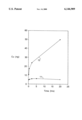
- the FIGURE is a plot of time in hours vs. weight of copper in nanograms showing the rate of deposition for a low concentration solution and a relatively high concentration solution.
- Sample wafers were placed in a high purity dilute HF solution for the first solvent extraction step. Dissolution was allowed to proceed for 2 minutes to dissolve the titanium film, and for an additional twenty minutes to ensure that metal ion impurities were allowed to reach electrochemical equilibrium with the bare silicon surface. The HF solution was analyzed and it was verified that the majority of titanium ions were in this solution.
- the surface of the bare silicon wafers at this point has a selective deposit of trace levels of copper.
- the tendency of copper to deposit from an HF solution onto a bare silicon surface is a phenomenon that has been recognized since the early days of silicon processing and in general has been regarded as an unwanted complication. Accordingly, any silicon IC processing steps that involve HF are incorporated carefully so as to minimize the possibility of copper contamination (i.e., ultra-high purity grade HF is used, and sometimes HCl is added to the HF solution to prevent copper plating).
- ultra-high purity grade HF is used, and sometimes HCl is added to the HF solution to prevent copper plating.
- the surface of the silicon wafers was rinsed with deionized water, and then treated with a second solvent for the second extraction step.
- the solvent in this case was chosen for copper detection and was a HNO 3 /HCl acid mixture.
- This extract solution was analyzed by ICP-MS. The results on four test wafers ranged from 2 to 5 ng of copper (per wafer), while titanium levels were less than0.01% of the original titanium quantity.
- trace levels of copper can be effectively separated from a background matrix of titanium so as to allow reliable and relatively precise detection of very low levels of these impurities.
- the preferred application for this technique is in testing for impurities during the manufacture of semiconductor devices.
- Those semiconductor devices may be semiconductor integrated circuits, or photonic devices such as lasers, optical integrated circuits, fiber amplifiers, etc.
- the semiconductor will be typically silicon or a III-V compound.
- the analytical procedure is conducted on sample wafers or control wafers that are processed through one or more stages in the wafer fabrication manufacturing line. The analysis of these test wafers may reveal a variety of conditions of interest to the process engineer.
- the test will be run after a metal deposition step to determine if the deposition apparatus is contaminated.
- the deposition apparatus may be a vacuum chamber used for evaporation or sputtering. If the contamination exceeds a desired level, the apparatus may be shut down and the source of the contamination removed.
- the silicon surface used to selectively deposit the copper trace impurities in the procedure described is the same surface as the semiconductor substrate on which the titanium layer is deposited.
- the semiconductor substrate being tested may be covered with other materials, e.g. field oxide, or interlevel dielectric, so the silicon surface used to adsorb the copper will be another silicon body, typically a bare silicon wafer.
- the semiconductor substrate on which the analysis is being conducted is another semiconductor, e.g. a III-V compound.
- the technique of the invention can also be implemented using polysilicon or amorphous silicon surfaces.
- deposition occurs most efficiently on single crystal material and that is the preferred choice for the invention. It is also preferred that the material be doped to a level in the range 1-50 ohm cm. Deposition appears to occur most rapidly on p-type silicon. The use of light, for example a halogen lamp, appears to accelerate the process.
Abstract
Description
Claims (12)
Priority Applications (1)
| Application Number | Priority Date | Filing Date | Title |
|---|---|---|---|
| US09/197,412 US6146909A (en) | 1998-11-21 | 1998-11-21 | Detecting trace levels of copper |
Applications Claiming Priority (1)
| Application Number | Priority Date | Filing Date | Title |
|---|---|---|---|
| US09/197,412 US6146909A (en) | 1998-11-21 | 1998-11-21 | Detecting trace levels of copper |
Publications (1)
| Publication Number | Publication Date |
|---|---|
| US6146909A true US6146909A (en) | 2000-11-14 |
Family
ID=22729323
Family Applications (1)
| Application Number | Title | Priority Date | Filing Date |
|---|---|---|---|
| US09/197,412 Expired - Lifetime US6146909A (en) | 1998-11-21 | 1998-11-21 | Detecting trace levels of copper |
Country Status (1)
| Country | Link |
|---|---|
| US (1) | US6146909A (en) |
Cited By (4)
| Publication number | Priority date | Publication date | Assignee | Title |
|---|---|---|---|---|
| US20070207616A1 (en) * | 2006-02-22 | 2007-09-06 | Katsuya Hirano | Method for assaying copper in silicon wafers |
| US20110146717A1 (en) * | 2009-12-23 | 2011-06-23 | Memc Electronic Materials, Inc. | Systems And Methods For Analysis of Water and Substrates Rinsed in Water |
| DE102004023425B4 (en) * | 2003-05-12 | 2017-08-24 | Sumco Corp. | Method for detecting the Cu concentration of a silicon substrate |
| CN112485090A (en) * | 2020-12-03 | 2021-03-12 | 西安奕斯伟硅片技术有限公司 | Method for testing copper content of silicon wafer |
-
1998
- 1998-11-21 US US09/197,412 patent/US6146909A/en not_active Expired - Lifetime
Cited By (5)
| Publication number | Priority date | Publication date | Assignee | Title |
|---|---|---|---|---|
| DE102004023425B4 (en) * | 2003-05-12 | 2017-08-24 | Sumco Corp. | Method for detecting the Cu concentration of a silicon substrate |
| US20070207616A1 (en) * | 2006-02-22 | 2007-09-06 | Katsuya Hirano | Method for assaying copper in silicon wafers |
| US7888265B2 (en) * | 2006-02-22 | 2011-02-15 | Sumco Corporation | Method for assaying copper in silicon wafers |
| US20110146717A1 (en) * | 2009-12-23 | 2011-06-23 | Memc Electronic Materials, Inc. | Systems And Methods For Analysis of Water and Substrates Rinsed in Water |
| CN112485090A (en) * | 2020-12-03 | 2021-03-12 | 西安奕斯伟硅片技术有限公司 | Method for testing copper content of silicon wafer |
Similar Documents
| Publication | Publication Date | Title |
|---|---|---|
| US7888265B2 (en) | Method for assaying copper in silicon wafers | |
| JP3494102B2 (en) | Evaluation method of metal impurity concentration in silicon wafer | |
| US6174740B1 (en) | Method for analyzing impurities within silicon wafer | |
| JP3044881B2 (en) | Method for analyzing metal impurities in surface oxide film of semiconductor substrate | |
| US6146909A (en) | Detecting trace levels of copper | |
| JPH10223713A (en) | Heat treatment evaluating wafer and heat treatment evaluating method using the same | |
| JP2012132779A (en) | Method for analyzing silicon sample | |
| Ferrero et al. | Improving the detection limits for vapor phase decomposition-inductively coupled plasma mass spectrometry (VPD-ICP-MS) analysis | |
| JP2973638B2 (en) | Impurity analysis method | |
| JP3331106B2 (en) | Method for analyzing impurities in semiconductor thin film or semiconductor substrate | |
| Rip et al. | Methodology for measuring trace metal surface contamination on PV silicon substrates | |
| Lu et al. | Evaluation of cleaning efficiency with a radioactive tracer and development of a microwave digestion method for semiconductor processes | |
| Wang et al. | Characterization and Modeling of Out‐Diffusion of Manganese and Zinc Impurities from Deep Ultraviolet Photoresist | |
| Rohatgi et al. | Characterization and control of silicon surface modification produced by CCl4 reactive ion etching | |
| KR100901823B1 (en) | Method of testing defect of silicon wafer | |
| Tan | Application of vapor phase decomposition techniques (VPD/AAS and ICP-MS) for trace element analysis in oxide coatings on silicon | |
| JP2004063721A (en) | Method for evaluating ni contamination in silicon wafer | |
| EP1542006B1 (en) | Impurity measuring method for GE substrates | |
| KR100999358B1 (en) | Method of estimating the concentration of metal contamination in wafer | |
| US20090277875A1 (en) | Method for the Determination of the Surface Occupation of a Silica Glass Component | |
| US6727189B2 (en) | Method for detecting metal contamination on a silicon chip by implanting arsenic | |
| JP4232457B2 (en) | Method for analyzing metal impurities in surface oxide film on silicon substrate surface | |
| Ketata et al. | A comparative secondary ion mass spectrometry technique for evaluation of metallic impurity on silicon surface | |
| JP2023133001A (en) | Method for analyzing polishing slurry for silicon wafer | |
| Mautz | Monitoring and reduction of alkali metal contamination in dielectric oxides |
Legal Events
| Date | Code | Title | Description |
|---|---|---|---|
| AS | Assignment |
Owner name: LUCENT TECHNOLOGIES INC., NEW JERSEY Free format text: ASSIGNMENT OF ASSIGNORS INTEREST;ASSIGNORS:ANTOL, JOZE E.;COULT, DAVID GERALD;DERKITS, GUSTAV EDWARD;AND OTHERS;REEL/FRAME:009609/0525;SIGNING DATES FROM 19981111 TO 19981119 |
|
| STCF | Information on status: patent grant |
Free format text: PATENTED CASE |
|
| FEPP | Fee payment procedure |
Free format text: PAYOR NUMBER ASSIGNED (ORIGINAL EVENT CODE: ASPN); ENTITY STATUS OF PATENT OWNER: LARGE ENTITY |
|
| FPAY | Fee payment |
Year of fee payment: 4 |
|
| FPAY | Fee payment |
Year of fee payment: 8 |
|
| FPAY | Fee payment |
Year of fee payment: 12 |
|
| AS | Assignment |
Owner name: DEUTSCHE BANK AG NEW YORK BRANCH, AS COLLATERAL AG Free format text: PATENT SECURITY AGREEMENT;ASSIGNORS:LSI CORPORATION;AGERE SYSTEMS LLC;REEL/FRAME:032856/0031 Effective date: 20140506 |
|
| AS | Assignment |
Owner name: AVAGO TECHNOLOGIES GENERAL IP (SINGAPORE) PTE. LTD Free format text: ASSIGNMENT OF ASSIGNORS INTEREST;ASSIGNOR:AGERE SYSTEMS LLC;REEL/FRAME:035365/0634 Effective date: 20140804 |
|
| AS | Assignment |
Owner name: LSI CORPORATION, CALIFORNIA Free format text: TERMINATION AND RELEASE OF SECURITY INTEREST IN PATENT RIGHTS (RELEASES RF 032856-0031);ASSIGNOR:DEUTSCHE BANK AG NEW YORK BRANCH, AS COLLATERAL AGENT;REEL/FRAME:037684/0039 Effective date: 20160201 Owner name: AGERE SYSTEMS LLC, PENNSYLVANIA Free format text: TERMINATION AND RELEASE OF SECURITY INTEREST IN PATENT RIGHTS (RELEASES RF 032856-0031);ASSIGNOR:DEUTSCHE BANK AG NEW YORK BRANCH, AS COLLATERAL AGENT;REEL/FRAME:037684/0039 Effective date: 20160201 |
|
| AS | Assignment |
Owner name: BANK OF AMERICA, N.A., AS COLLATERAL AGENT, NORTH CAROLINA Free format text: PATENT SECURITY AGREEMENT;ASSIGNOR:AVAGO TECHNOLOGIES GENERAL IP (SINGAPORE) PTE. LTD.;REEL/FRAME:037808/0001 Effective date: 20160201 Owner name: BANK OF AMERICA, N.A., AS COLLATERAL AGENT, NORTH Free format text: PATENT SECURITY AGREEMENT;ASSIGNOR:AVAGO TECHNOLOGIES GENERAL IP (SINGAPORE) PTE. LTD.;REEL/FRAME:037808/0001 Effective date: 20160201 |
|
| AS | Assignment |
Owner name: AVAGO TECHNOLOGIES GENERAL IP (SINGAPORE) PTE. LTD., SINGAPORE Free format text: TERMINATION AND RELEASE OF SECURITY INTEREST IN PATENTS;ASSIGNOR:BANK OF AMERICA, N.A., AS COLLATERAL AGENT;REEL/FRAME:041710/0001 Effective date: 20170119 Owner name: AVAGO TECHNOLOGIES GENERAL IP (SINGAPORE) PTE. LTD Free format text: TERMINATION AND RELEASE OF SECURITY INTEREST IN PATENTS;ASSIGNOR:BANK OF AMERICA, N.A., AS COLLATERAL AGENT;REEL/FRAME:041710/0001 Effective date: 20170119 |
|
| AS | Assignment |
Owner name: BELL SEMICONDUCTOR, LLC, ILLINOIS Free format text: ASSIGNMENT OF ASSIGNORS INTEREST;ASSIGNORS:AVAGO TECHNOLOGIES GENERAL IP (SINGAPORE) PTE. LTD.;BROADCOM CORPORATION;REEL/FRAME:044886/0608 Effective date: 20171208 |
|
| AS | Assignment |
Owner name: CORTLAND CAPITAL MARKET SERVICES LLC, AS COLLATERA Free format text: SECURITY INTEREST;ASSIGNORS:HILCO PATENT ACQUISITION 56, LLC;BELL SEMICONDUCTOR, LLC;BELL NORTHERN RESEARCH, LLC;REEL/FRAME:045216/0020 Effective date: 20180124 |
|
| AS | Assignment |
Owner name: BELL NORTHERN RESEARCH, LLC, ILLINOIS Free format text: RELEASE BY SECURED PARTY;ASSIGNOR:CORTLAND CAPITAL MARKET SERVICES LLC;REEL/FRAME:059720/0719 Effective date: 20220401 Owner name: BELL SEMICONDUCTOR, LLC, ILLINOIS Free format text: RELEASE BY SECURED PARTY;ASSIGNOR:CORTLAND CAPITAL MARKET SERVICES LLC;REEL/FRAME:059720/0719 Effective date: 20220401 Owner name: HILCO PATENT ACQUISITION 56, LLC, ILLINOIS Free format text: RELEASE BY SECURED PARTY;ASSIGNOR:CORTLAND CAPITAL MARKET SERVICES LLC;REEL/FRAME:059720/0719 Effective date: 20220401 |