US6033935A - Sockets for "springed" semiconductor devices - Google Patents
Sockets for "springed" semiconductor devices Download PDFInfo
- Publication number
- US6033935A US6033935A US09/108,163 US10816398A US6033935A US 6033935 A US6033935 A US 6033935A US 10816398 A US10816398 A US 10816398A US 6033935 A US6033935 A US 6033935A
- Authority
- US
- United States
- Prior art keywords
- spring contact
- interconnection substrate
- terminals
- contact elements
- semiconductor device
- Prior art date
- Legal status (The legal status is an assumption and is not a legal conclusion. Google has not performed a legal analysis and makes no representation as to the accuracy of the status listed.)
- Expired - Fee Related
Links
Images


Classifications
-
- G—PHYSICS
- G01—MEASURING; TESTING
- G01R—MEASURING ELECTRIC VARIABLES; MEASURING MAGNETIC VARIABLES
- G01R1/00—Details of instruments or arrangements of the types included in groups G01R5/00 - G01R13/00 and G01R31/00
- G01R1/02—General constructional details
- G01R1/04—Housings; Supporting members; Arrangements of terminals
- G01R1/0408—Test fixtures or contact fields; Connectors or connecting adaptors; Test clips; Test sockets
-
- B—PERFORMING OPERATIONS; TRANSPORTING
- B23—MACHINE TOOLS; METAL-WORKING NOT OTHERWISE PROVIDED FOR
- B23K—SOLDERING OR UNSOLDERING; WELDING; CLADDING OR PLATING BY SOLDERING OR WELDING; CUTTING BY APPLYING HEAT LOCALLY, e.g. FLAME CUTTING; WORKING BY LASER BEAM
- B23K3/00—Tools, devices, or special appurtenances for soldering, e.g. brazing, or unsoldering, not specially adapted for particular methods
- B23K3/08—Auxiliary devices therefor
- B23K3/087—Soldering or brazing jigs, fixtures or clamping means
-
- G—PHYSICS
- G01—MEASURING; TESTING
- G01R—MEASURING ELECTRIC VARIABLES; MEASURING MAGNETIC VARIABLES
- G01R1/00—Details of instruments or arrangements of the types included in groups G01R5/00 - G01R13/00 and G01R31/00
- G01R1/02—General constructional details
- G01R1/04—Housings; Supporting members; Arrangements of terminals
- G01R1/0408—Test fixtures or contact fields; Connectors or connecting adaptors; Test clips; Test sockets
- G01R1/0433—Sockets for IC's or transistors
- G01R1/0441—Details
- G01R1/0466—Details concerning contact pieces or mechanical details, e.g. hinges or cams; Shielding
-
- G—PHYSICS
- G01—MEASURING; TESTING
- G01R—MEASURING ELECTRIC VARIABLES; MEASURING MAGNETIC VARIABLES
- G01R31/00—Arrangements for testing electric properties; Arrangements for locating electric faults; Arrangements for electrical testing characterised by what is being tested not provided for elsewhere
- G01R31/28—Testing of electronic circuits, e.g. by signal tracer
- G01R31/2851—Testing of integrated circuits [IC]
- G01R31/2886—Features relating to contacting the IC under test, e.g. probe heads; chucks
-
- H—ELECTRICITY
- H01—ELECTRIC ELEMENTS
- H01L—SEMICONDUCTOR DEVICES NOT COVERED BY CLASS H10
- H01L23/00—Details of semiconductor or other solid state devices
- H01L23/02—Containers; Seals
- H01L23/04—Containers; Seals characterised by the shape of the container or parts, e.g. caps, walls
-
- H—ELECTRICITY
- H01—ELECTRIC ELEMENTS
- H01L—SEMICONDUCTOR DEVICES NOT COVERED BY CLASS H10
- H01L23/00—Details of semiconductor or other solid state devices
- H01L23/12—Mountings, e.g. non-detachable insulating substrates
- H01L23/13—Mountings, e.g. non-detachable insulating substrates characterised by the shape
-
- H—ELECTRICITY
- H01—ELECTRIC ELEMENTS
- H01L—SEMICONDUCTOR DEVICES NOT COVERED BY CLASS H10
- H01L23/00—Details of semiconductor or other solid state devices
- H01L23/32—Holders for supporting the complete device in operation, i.e. detachable fixtures
-
- H—ELECTRICITY
- H01—ELECTRIC ELEMENTS
- H01L—SEMICONDUCTOR DEVICES NOT COVERED BY CLASS H10
- H01L23/00—Details of semiconductor or other solid state devices
- H01L23/52—Arrangements for conducting electric current within the device in operation from one component to another, i.e. interconnections, e.g. wires, lead frames
- H01L23/538—Arrangements for conducting electric current within the device in operation from one component to another, i.e. interconnections, e.g. wires, lead frames the interconnection structure between a plurality of semiconductor chips being formed on, or in, insulating substrates
- H01L23/5385—Assembly of a plurality of insulating substrates
-
- H—ELECTRICITY
- H01—ELECTRIC ELEMENTS
- H01L—SEMICONDUCTOR DEVICES NOT COVERED BY CLASS H10
- H01L24/00—Arrangements for connecting or disconnecting semiconductor or solid-state bodies; Methods or apparatus related thereto
- H01L24/71—Means for bonding not being attached to, or not being formed on, the surface to be connected
- H01L24/72—Detachable connecting means consisting of mechanical auxiliary parts connecting the device, e.g. pressure contacts using springs or clips
-
- H—ELECTRICITY
- H05—ELECTRIC TECHNIQUES NOT OTHERWISE PROVIDED FOR
- H05K—PRINTED CIRCUITS; CASINGS OR CONSTRUCTIONAL DETAILS OF ELECTRIC APPARATUS; MANUFACTURE OF ASSEMBLAGES OF ELECTRICAL COMPONENTS
- H05K3/00—Apparatus or processes for manufacturing printed circuits
- H05K3/30—Assembling printed circuits with electric components, e.g. with resistor
- H05K3/306—Lead-in-hole components, e.g. affixing or retention before soldering, spacing means
- H05K3/308—Adaptations of leads
-
- H—ELECTRICITY
- H05—ELECTRIC TECHNIQUES NOT OTHERWISE PROVIDED FOR
- H05K—PRINTED CIRCUITS; CASINGS OR CONSTRUCTIONAL DETAILS OF ELECTRIC APPARATUS; MANUFACTURE OF ASSEMBLAGES OF ELECTRICAL COMPONENTS
- H05K3/00—Apparatus or processes for manufacturing printed circuits
- H05K3/30—Assembling printed circuits with electric components, e.g. with resistor
- H05K3/32—Assembling printed circuits with electric components, e.g. with resistor electrically connecting electric components or wires to printed circuits
- H05K3/325—Assembling printed circuits with electric components, e.g. with resistor electrically connecting electric components or wires to printed circuits by abutting or pinching, i.e. without alloying process; mechanical auxiliary parts therefor
-
- G—PHYSICS
- G01—MEASURING; TESTING
- G01R—MEASURING ELECTRIC VARIABLES; MEASURING MAGNETIC VARIABLES
- G01R1/00—Details of instruments or arrangements of the types included in groups G01R5/00 - G01R13/00 and G01R31/00
- G01R1/02—General constructional details
- G01R1/04—Housings; Supporting members; Arrangements of terminals
- G01R1/0408—Test fixtures or contact fields; Connectors or connecting adaptors; Test clips; Test sockets
- G01R1/0416—Connectors, terminals
-
- H—ELECTRICITY
- H01—ELECTRIC ELEMENTS
- H01L—SEMICONDUCTOR DEVICES NOT COVERED BY CLASS H10
- H01L2224/00—Indexing scheme for arrangements for connecting or disconnecting semiconductor or solid-state bodies and methods related thereto as covered by H01L24/00
- H01L2224/01—Means for bonding being attached to, or being formed on, the surface to be connected, e.g. chip-to-package, die-attach, "first-level" interconnects; Manufacturing methods related thereto
- H01L2224/10—Bump connectors; Manufacturing methods related thereto
- H01L2224/11—Manufacturing methods
- H01L2224/113—Manufacturing methods by local deposition of the material of the bump connector
- H01L2224/1133—Manufacturing methods by local deposition of the material of the bump connector in solid form
- H01L2224/1134—Stud bumping, i.e. using a wire-bonding apparatus
-
- H—ELECTRICITY
- H01—ELECTRIC ELEMENTS
- H01L—SEMICONDUCTOR DEVICES NOT COVERED BY CLASS H10
- H01L2224/00—Indexing scheme for arrangements for connecting or disconnecting semiconductor or solid-state bodies and methods related thereto as covered by H01L24/00
- H01L2224/01—Means for bonding being attached to, or being formed on, the surface to be connected, e.g. chip-to-package, die-attach, "first-level" interconnects; Manufacturing methods related thereto
- H01L2224/10—Bump connectors; Manufacturing methods related thereto
- H01L2224/12—Structure, shape, material or disposition of the bump connectors prior to the connecting process
- H01L2224/13—Structure, shape, material or disposition of the bump connectors prior to the connecting process of an individual bump connector
- H01L2224/13001—Core members of the bump connector
- H01L2224/13099—Material
-
- H—ELECTRICITY
- H01—ELECTRIC ELEMENTS
- H01L—SEMICONDUCTOR DEVICES NOT COVERED BY CLASS H10
- H01L2224/00—Indexing scheme for arrangements for connecting or disconnecting semiconductor or solid-state bodies and methods related thereto as covered by H01L24/00
- H01L2224/01—Means for bonding being attached to, or being formed on, the surface to be connected, e.g. chip-to-package, die-attach, "first-level" interconnects; Manufacturing methods related thereto
- H01L2224/10—Bump connectors; Manufacturing methods related thereto
- H01L2224/15—Structure, shape, material or disposition of the bump connectors after the connecting process
- H01L2224/16—Structure, shape, material or disposition of the bump connectors after the connecting process of an individual bump connector
- H01L2224/161—Disposition
- H01L2224/16151—Disposition the bump connector connecting between a semiconductor or solid-state body and an item not being a semiconductor or solid-state body, e.g. chip-to-substrate, chip-to-passive
- H01L2224/16221—Disposition the bump connector connecting between a semiconductor or solid-state body and an item not being a semiconductor or solid-state body, e.g. chip-to-substrate, chip-to-passive the body and the item being stacked
- H01L2224/16225—Disposition the bump connector connecting between a semiconductor or solid-state body and an item not being a semiconductor or solid-state body, e.g. chip-to-substrate, chip-to-passive the body and the item being stacked the item being non-metallic, e.g. insulating substrate with or without metallisation
- H01L2224/16237—Disposition the bump connector connecting between a semiconductor or solid-state body and an item not being a semiconductor or solid-state body, e.g. chip-to-substrate, chip-to-passive the body and the item being stacked the item being non-metallic, e.g. insulating substrate with or without metallisation the bump connector connecting to a bonding area disposed in a recess of the surface of the item
-
- H—ELECTRICITY
- H01—ELECTRIC ELEMENTS
- H01L—SEMICONDUCTOR DEVICES NOT COVERED BY CLASS H10
- H01L2224/00—Indexing scheme for arrangements for connecting or disconnecting semiconductor or solid-state bodies and methods related thereto as covered by H01L24/00
- H01L2224/73—Means for bonding being of different types provided for in two or more of groups H01L2224/10, H01L2224/18, H01L2224/26, H01L2224/34, H01L2224/42, H01L2224/50, H01L2224/63, H01L2224/71
- H01L2224/732—Location after the connecting process
- H01L2224/73251—Location after the connecting process on different surfaces
-
- H—ELECTRICITY
- H01—ELECTRIC ELEMENTS
- H01L—SEMICONDUCTOR DEVICES NOT COVERED BY CLASS H10
- H01L2224/00—Indexing scheme for arrangements for connecting or disconnecting semiconductor or solid-state bodies and methods related thereto as covered by H01L24/00
- H01L2224/80—Methods for connecting semiconductor or other solid state bodies using means for bonding being attached to, or being formed on, the surface to be connected
- H01L2224/81—Methods for connecting semiconductor or other solid state bodies using means for bonding being attached to, or being formed on, the surface to be connected using a bump connector
- H01L2224/8112—Aligning
- H01L2224/81136—Aligning involving guiding structures, e.g. spacers or supporting members
- H01L2224/81138—Aligning involving guiding structures, e.g. spacers or supporting members the guiding structures being at least partially left in the finished device
- H01L2224/8114—Guiding structures outside the body
-
- H—ELECTRICITY
- H01—ELECTRIC ELEMENTS
- H01L—SEMICONDUCTOR DEVICES NOT COVERED BY CLASS H10
- H01L2224/00—Indexing scheme for arrangements for connecting or disconnecting semiconductor or solid-state bodies and methods related thereto as covered by H01L24/00
- H01L2224/80—Methods for connecting semiconductor or other solid state bodies using means for bonding being attached to, or being formed on, the surface to be connected
- H01L2224/81—Methods for connecting semiconductor or other solid state bodies using means for bonding being attached to, or being formed on, the surface to be connected using a bump connector
- H01L2224/819—Methods for connecting semiconductor or other solid state bodies using means for bonding being attached to, or being formed on, the surface to be connected using a bump connector with the bump connector not providing any mechanical bonding
- H01L2224/81901—Pressing the bump connector against the bonding areas by means of another connector
-
- H—ELECTRICITY
- H01—ELECTRIC ELEMENTS
- H01L—SEMICONDUCTOR DEVICES NOT COVERED BY CLASS H10
- H01L2924/00—Indexing scheme for arrangements or methods for connecting or disconnecting semiconductor or solid-state bodies as covered by H01L24/00
- H01L2924/0001—Technical content checked by a classifier
- H01L2924/00013—Fully indexed content
-
- H—ELECTRICITY
- H01—ELECTRIC ELEMENTS
- H01L—SEMICONDUCTOR DEVICES NOT COVERED BY CLASS H10
- H01L2924/00—Indexing scheme for arrangements or methods for connecting or disconnecting semiconductor or solid-state bodies as covered by H01L24/00
- H01L2924/01—Chemical elements
- H01L2924/01006—Carbon [C]
-
- H—ELECTRICITY
- H01—ELECTRIC ELEMENTS
- H01L—SEMICONDUCTOR DEVICES NOT COVERED BY CLASS H10
- H01L2924/00—Indexing scheme for arrangements or methods for connecting or disconnecting semiconductor or solid-state bodies as covered by H01L24/00
- H01L2924/01—Chemical elements
- H01L2924/01013—Aluminum [Al]
-
- H—ELECTRICITY
- H01—ELECTRIC ELEMENTS
- H01L—SEMICONDUCTOR DEVICES NOT COVERED BY CLASS H10
- H01L2924/00—Indexing scheme for arrangements or methods for connecting or disconnecting semiconductor or solid-state bodies as covered by H01L24/00
- H01L2924/01—Chemical elements
- H01L2924/01023—Vanadium [V]
-
- H—ELECTRICITY
- H01—ELECTRIC ELEMENTS
- H01L—SEMICONDUCTOR DEVICES NOT COVERED BY CLASS H10
- H01L2924/00—Indexing scheme for arrangements or methods for connecting or disconnecting semiconductor or solid-state bodies as covered by H01L24/00
- H01L2924/01—Chemical elements
- H01L2924/01029—Copper [Cu]
-
- H—ELECTRICITY
- H01—ELECTRIC ELEMENTS
- H01L—SEMICONDUCTOR DEVICES NOT COVERED BY CLASS H10
- H01L2924/00—Indexing scheme for arrangements or methods for connecting or disconnecting semiconductor or solid-state bodies as covered by H01L24/00
- H01L2924/01—Chemical elements
- H01L2924/01033—Arsenic [As]
-
- H—ELECTRICITY
- H01—ELECTRIC ELEMENTS
- H01L—SEMICONDUCTOR DEVICES NOT COVERED BY CLASS H10
- H01L2924/00—Indexing scheme for arrangements or methods for connecting or disconnecting semiconductor or solid-state bodies as covered by H01L24/00
- H01L2924/01—Chemical elements
- H01L2924/01039—Yttrium [Y]
-
- H—ELECTRICITY
- H01—ELECTRIC ELEMENTS
- H01L—SEMICONDUCTOR DEVICES NOT COVERED BY CLASS H10
- H01L2924/00—Indexing scheme for arrangements or methods for connecting or disconnecting semiconductor or solid-state bodies as covered by H01L24/00
- H01L2924/01—Chemical elements
- H01L2924/01078—Platinum [Pt]
-
- H—ELECTRICITY
- H01—ELECTRIC ELEMENTS
- H01L—SEMICONDUCTOR DEVICES NOT COVERED BY CLASS H10
- H01L2924/00—Indexing scheme for arrangements or methods for connecting or disconnecting semiconductor or solid-state bodies as covered by H01L24/00
- H01L2924/01—Chemical elements
- H01L2924/01079—Gold [Au]
-
- H—ELECTRICITY
- H05—ELECTRIC TECHNIQUES NOT OTHERWISE PROVIDED FOR
- H05K—PRINTED CIRCUITS; CASINGS OR CONSTRUCTIONAL DETAILS OF ELECTRIC APPARATUS; MANUFACTURE OF ASSEMBLAGES OF ELECTRICAL COMPONENTS
- H05K1/00—Printed circuits
- H05K1/02—Details
- H05K1/11—Printed elements for providing electric connections to or between printed circuits
- H05K1/119—Details of rigid insulating substrates therefor, e.g. three-dimensional details
-
- H—ELECTRICITY
- H05—ELECTRIC TECHNIQUES NOT OTHERWISE PROVIDED FOR
- H05K—PRINTED CIRCUITS; CASINGS OR CONSTRUCTIONAL DETAILS OF ELECTRIC APPARATUS; MANUFACTURE OF ASSEMBLAGES OF ELECTRICAL COMPONENTS
- H05K2201/00—Indexing scheme relating to printed circuits covered by H05K1/00
- H05K2201/03—Conductive materials
- H05K2201/0302—Properties and characteristics in general
- H05K2201/0311—Metallic part with specific elastic properties, e.g. bent piece of metal as electrical contact
-
- H—ELECTRICITY
- H05—ELECTRIC TECHNIQUES NOT OTHERWISE PROVIDED FOR
- H05K—PRINTED CIRCUITS; CASINGS OR CONSTRUCTIONAL DETAILS OF ELECTRIC APPARATUS; MANUFACTURE OF ASSEMBLAGES OF ELECTRICAL COMPONENTS
- H05K2201/00—Indexing scheme relating to printed circuits covered by H05K1/00
- H05K2201/09—Shape and layout
- H05K2201/09209—Shape and layout details of conductors
- H05K2201/09372—Pads and lands
- H05K2201/09472—Recessed pad for surface mounting; Recessed electrode of component
-
- H—ELECTRICITY
- H05—ELECTRIC TECHNIQUES NOT OTHERWISE PROVIDED FOR
- H05K—PRINTED CIRCUITS; CASINGS OR CONSTRUCTIONAL DETAILS OF ELECTRIC APPARATUS; MANUFACTURE OF ASSEMBLAGES OF ELECTRICAL COMPONENTS
- H05K2201/00—Indexing scheme relating to printed circuits covered by H05K1/00
- H05K2201/09—Shape and layout
- H05K2201/09818—Shape or layout details not covered by a single group of H05K2201/09009 - H05K2201/09809
- H05K2201/09827—Tapered, e.g. tapered hole, via or groove
-
- Y—GENERAL TAGGING OF NEW TECHNOLOGICAL DEVELOPMENTS; GENERAL TAGGING OF CROSS-SECTIONAL TECHNOLOGIES SPANNING OVER SEVERAL SECTIONS OF THE IPC; TECHNICAL SUBJECTS COVERED BY FORMER USPC CROSS-REFERENCE ART COLLECTIONS [XRACs] AND DIGESTS
- Y10—TECHNICAL SUBJECTS COVERED BY FORMER USPC
- Y10T—TECHNICAL SUBJECTS COVERED BY FORMER US CLASSIFICATION
- Y10T29/00—Metal working
- Y10T29/49—Method of mechanical manufacture
- Y10T29/49002—Electrical device making
- Y10T29/49117—Conductor or circuit manufacturing
- Y10T29/49124—On flat or curved insulated base, e.g., printed circuit, etc.
- Y10T29/49128—Assembling formed circuit to base
-
- Y—GENERAL TAGGING OF NEW TECHNOLOGICAL DEVELOPMENTS; GENERAL TAGGING OF CROSS-SECTIONAL TECHNOLOGIES SPANNING OVER SEVERAL SECTIONS OF THE IPC; TECHNICAL SUBJECTS COVERED BY FORMER USPC CROSS-REFERENCE ART COLLECTIONS [XRACs] AND DIGESTS
- Y10—TECHNICAL SUBJECTS COVERED BY FORMER USPC
- Y10T—TECHNICAL SUBJECTS COVERED BY FORMER US CLASSIFICATION
- Y10T29/00—Metal working
- Y10T29/49—Method of mechanical manufacture
- Y10T29/49002—Electrical device making
- Y10T29/49117—Conductor or circuit manufacturing
- Y10T29/49124—On flat or curved insulated base, e.g., printed circuit, etc.
- Y10T29/4913—Assembling to base an electrical component, e.g., capacitor, etc.
- Y10T29/49139—Assembling to base an electrical component, e.g., capacitor, etc. by inserting component lead or terminal into base aperture
- Y10T29/4914—Assembling to base an electrical component, e.g., capacitor, etc. by inserting component lead or terminal into base aperture with deforming of lead or terminal
-
- Y—GENERAL TAGGING OF NEW TECHNOLOGICAL DEVELOPMENTS; GENERAL TAGGING OF CROSS-SECTIONAL TECHNOLOGIES SPANNING OVER SEVERAL SECTIONS OF THE IPC; TECHNICAL SUBJECTS COVERED BY FORMER USPC CROSS-REFERENCE ART COLLECTIONS [XRACs] AND DIGESTS
- Y10—TECHNICAL SUBJECTS COVERED BY FORMER USPC
- Y10T—TECHNICAL SUBJECTS COVERED BY FORMER US CLASSIFICATION
- Y10T29/00—Metal working
- Y10T29/49—Method of mechanical manufacture
- Y10T29/49002—Electrical device making
- Y10T29/49117—Conductor or circuit manufacturing
- Y10T29/49124—On flat or curved insulated base, e.g., printed circuit, etc.
- Y10T29/49147—Assembling terminal to base
- Y10T29/49151—Assembling terminal to base by deforming or shaping
- Y10T29/49153—Assembling terminal to base by deforming or shaping with shaping or forcing terminal into base aperture
-
- Y—GENERAL TAGGING OF NEW TECHNOLOGICAL DEVELOPMENTS; GENERAL TAGGING OF CROSS-SECTIONAL TECHNOLOGIES SPANNING OVER SEVERAL SECTIONS OF THE IPC; TECHNICAL SUBJECTS COVERED BY FORMER USPC CROSS-REFERENCE ART COLLECTIONS [XRACs] AND DIGESTS
- Y10—TECHNICAL SUBJECTS COVERED BY FORMER USPC
- Y10T—TECHNICAL SUBJECTS COVERED BY FORMER US CLASSIFICATION
- Y10T29/00—Metal working
- Y10T29/49—Method of mechanical manufacture
- Y10T29/49002—Electrical device making
- Y10T29/49117—Conductor or circuit manufacturing
- Y10T29/49204—Contact or terminal manufacturing
- Y10T29/49208—Contact or terminal manufacturing by assembling plural parts
-
- Y—GENERAL TAGGING OF NEW TECHNOLOGICAL DEVELOPMENTS; GENERAL TAGGING OF CROSS-SECTIONAL TECHNOLOGIES SPANNING OVER SEVERAL SECTIONS OF THE IPC; TECHNICAL SUBJECTS COVERED BY FORMER USPC CROSS-REFERENCE ART COLLECTIONS [XRACs] AND DIGESTS
- Y10—TECHNICAL SUBJECTS COVERED BY FORMER USPC
- Y10T—TECHNICAL SUBJECTS COVERED BY FORMER US CLASSIFICATION
- Y10T29/00—Metal working
- Y10T29/53—Means to assemble or disassemble
- Y10T29/5313—Means to assemble electrical device
- Y10T29/53174—Means to fasten electrical component to wiring board, base, or substrate
- Y10T29/53178—Chip component
-
- Y—GENERAL TAGGING OF NEW TECHNOLOGICAL DEVELOPMENTS; GENERAL TAGGING OF CROSS-SECTIONAL TECHNOLOGIES SPANNING OVER SEVERAL SECTIONS OF THE IPC; TECHNICAL SUBJECTS COVERED BY FORMER USPC CROSS-REFERENCE ART COLLECTIONS [XRACs] AND DIGESTS
- Y10—TECHNICAL SUBJECTS COVERED BY FORMER USPC
- Y10T—TECHNICAL SUBJECTS COVERED BY FORMER US CLASSIFICATION
- Y10T29/00—Metal working
- Y10T29/53—Means to assemble or disassemble
- Y10T29/5313—Means to assemble electrical device
- Y10T29/53174—Means to fasten electrical component to wiring board, base, or substrate
- Y10T29/53183—Multilead component
Definitions
- the invention relates to making interconnections between electronic components, especially microelectronic components and, more particularly, to interconnection elements (contact structures) exhibiting resiliency (springiness), and methods of making same.
- KHANDROS disclose methods for making resilient interconnection elements for microelectronics applications involving mounting an end of a flexible elongate core element (e.g., wire "stem” or “skeletons") to a terminal on an electronic component, coating the flexible core element and adjacent surface of the terminal with a "shell" of one or more materials having a predetermined combination of thickness, yield strength and elastic modulus to ensure predetermined force-to-deflection characteristics of the resulting spring contacts.
- exemplary materials for the core element include gold.
- Exemplary materials for the coating include nickel and its alloys.
- the resulting spring contact element is suitably used to effect pressure, or demountable, connections between two or more electronic components, including semiconductor devices.
- the present invention addresses and is particularly well-suited to making interconnections to modern microelectronic devices having their terminals (bond pads) disposed at a fine-pitch.
- fine-pitch refers to microelectronic devices that have their terminals disposed at a spacing of less than 5 mils, such as 2.5 mils or 65 ⁇ m. As will be evident from the description that follows, this is preferably achieved by taking advantage of the close tolerances that readily can be realized by using lithographic rather than mechanical techniques to fabricate the contact elements.
- a semiconductor device having spring contact elements mounted thereto is termed a “springed semiconductor device”.
- Such a device may be interconnected to an interconnection substrate in one of two main ways. It may be “permanently” connected such as by soldering the free ends of the spring contact elements to corresponding terminals on an interconnection substrate such as a printed circuit board. Alternatively, it may be “temporarily” connected to the terminals simply by urging the springed semiconductor device against the interconnection substrate so that a pressure connection is made between the free ends of the spring contact elements and the terminals. Another way of looking at such temporary pressure connections is that the springed semiconductor device is "self-socketing".
- a certain minimum contact force is desired to effect reliable pressure contact to electronic components (e.g., to terminals on electronic components) .
- a contact (load) force of approximately 15 grams (including as little as 2 grams or less and as much as 150 grams or more, per contact) may be desired to ensure that a reliable electrical connection is made to a terminal of an electronic component which may be contaminated with films on its surface, or which has corrosion or oxidation products on its surface.
- each spring contact element demands either that the yield strength of the spring material or that the size of the spring element are increased.
- the higher the yield strength of a material the more difficult it will be to work with (e.g., punch, bend, etc.).
- the desire to make springs smaller essentially rules out making them larger in cross-section.
- a more fundamental object is achieved simply by making transient (very temporary) connections to a springed semiconductor device. And that is, the ability to test the springed semiconductor device prior to temporarily or permanently mounting it to an interconnection substrate of a system to (1), if necessary, burn-in the springed semiconductor device and (2) to ascertain whether the springed semiconductor device is measuring up to its specifications. As a general proposition, this can be accomplished by making "transient" pressure connections with the spring contact elements with relaxed constraints on contact force and the like. The making of such transient connections to springed semiconductor devices is the focus of the present invention.
- the present invention discloses a number of techniques for socketing (making transient pressure connections) to springed semiconductor devices.
- an interconnection substrate has a terminal which is a plated through hole.
- the spring contact element is inserted through the through hole so that a portion of the spring contact element is within the through hole.
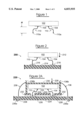
- FIG. 1 is a side cross-sectional view of a "springed" semiconductor device, according to the invention.
- a springed semiconductor device is shown with spring contact elements which are mounted thereto and extend therefrom contacting corresponding terminals of an interconnection substrate.
- the spring contact elements are shown contacting the terminals.
- Other of the figures are slightly exploded for illustrative clarity, showing the spring contact elements nearly in contact with the terminals.
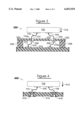
- FIG. 2 is a side cross-sectional view of a "springed" semiconductor device being urged against an interconnection substrate such as a printed circuit board (PCB), according to the invention.
- PCB printed circuit board
- FIG. 2A is a side cross-sectional view of another technique of urging a springed semiconductor device against an interconnection substrate, according to the invention.
- FIG. 3 is a side cross-sectional view of another technique of urging a springed semiconductor device into contact with terminals of an interconnection substrate, according to the invention.
- FIG. 4 is a side cross-sectional view of another technique of connecting a springed semiconductor device to terminals of an interconnection substrate, according to the invention.
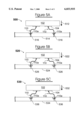
- FIG. 5A is a side cross-sectional view of a technique of urging a springed semiconductor device into contact with concave terminals of an interconnection substrate, according to the invention.
- FIG. 5B is a side cross-sectional view of another technique of urging a springed semiconductor device into contact with concave terminals of an interconnection substrate, according to the invention.
- FIG. 5C is a side cross-sectional view of another technique of urging a springed semiconductor device into contact with concave terminals of an interconnection substrate, according to the invention.
- FIG. 6A is a side cross-sectional view of another technique of horizontally contacting spring contact elements extending from a springed semiconductor device with resilient contact structures extending from terminals of an interconnection substrate, according to the invention.
- FIG. 6B is a bottom plan view of the apparatus of FIG. 6A, according to the invention.
- FIG. 7A is a side cross-sectional view of another technique of horizontally contacting spring contact elements extending from a springed semiconductor device with pairs of resilient contact structures extending from terminals of an interconnection substrate, according to the invention.
- FIG. 7B is a bottom plan view of the apparatus of FIG. 7A, according to the invention.
- FIG. 7C is a bottom plan view of an alternate embodiment of the apparatus of FIG. 7A, according to the invention.
- FIG. 8 is a side cross-sectional view of another technique of horizontally contacting spring contact elements extending from a springed semiconductor device with terminals of an interconnection substrate, according to the invention.
- FIGS. 9A and 9B are side cross-sectional views of another technique of horizontally contacting spring contact elements extending from a springed semiconductor device with terminals of an interconnection substrate, according to the invention.
- FIG. 1 illustrates a "springed" semiconductor device 102, which is an electronic component having a plurality (two of many shown) of free-standing elongate microspring spring contact structures 110 mounted to and extending from a corresponding plurality (two of many shown) of terminals 104 on a surface thereof.
- Each spring contact element 110 extends laterally parallel to the surface of the component 102 (in the “x” and “y” axes, and extends to a height “H” in the z-axis above the surface of the component 102.
- the springed semiconductor device 102 can be connected to another electronic component such as a printed circuit board (PCB) or other suitable interconnection substrate simply by urging the free ends (tips) 110a of the spring contact elements 110 against corresponding terminals (not shown) on the PCB (not shown).
- the free ends (tips) of the spring contact elements 110 can be soldered to the terminals of the PCB or interconnection substrate.
- FIG. 2 illustrates a technique 200 wherein the "springed" semiconductor device 102 is urged (in the direction of the arrow 212) against an interconnection substrate such as a printed circuit board (PCB) 214 so that the tips 110a come into pressure contact with a corresponding plurality (two of many shown) of terminals 216 on the PCB 214 to establish a pressure connection therewith.
- the tips 110a of the spring contact elements 110 can also be soldered to the terminals 216 of the PCB 214.
- the present invention is principally directed to making temporary connections with the spring contact elements (110) of springed semiconductor devices (102).
- FIG. 2 and the figures that follow, are illustrative of making temporary pressure connections to a springed semiconductor device such as for testing the semiconductor device.
- the semiconductor device is termed a "device under test" (DUT).
- DUT device under test
- the temporary pressure connection is made in the z-axis, by applying "vertical" pressure to the tip (110a) of the spring contact element (110) in a direction which is perpendicular to the surface of the electronic component 102.
- the temporary pressure connection is made in the x or y axes, by applying "horizontal" pressure to a midportion of the spring contact element (110) in a direction which is parallel to the surface of the electronic component 102.
- FIG. 2A illustrates another technique 220 for making a vertical temporary pressure connection with spring contact elements 110 of a springed semiconductor device (DUT) 102.
- the tips 110a of the spring contact elements 110 make pressure connections (contact) with terminals 226 (compare 216) of a PCB 224 (compare 214), as illustrated by the arrow 228 (compare 212).
- the DUT 102 is housed within a metal cap (housing) 230 which is a five-sided box such that the back side (top, as viewed) of the DUT is against the bottom surface of the housing 230.
- the open (bottom, as viewed) end of the housing 230 is covered by a rigid planar member (substrate) 232 which has a plurality (two of many shown) of guide holes 234 aligned with the tips 110a of the spring contact elements 110 which extend therethrough.
- a rigid planar member (substrate) 232 which has a plurality (two of many shown) of guide holes 234 aligned with the tips 110a of the spring contact elements 110 which extend therethrough.
- the spring contact elements 110 extend 5 mils beyond the external (bottom, as viewed) surface of the rigid planar substrate 232.
- the rigid planar substrate 232 is suitably formed of silicon and the guide holes are suitably tapered with their wide ends facing the DUT 102 and the interior of the housing 230, and is suitably formed of a silicon wafer using conventional semiconductor micromachining techniques. As illustrated, the rigid planar substrate 232 is sized to extend slightly, such as 100-250 mils beyond the four (two visible in the figure) sidewalls of the housing 230, to completely cover the open (bottom, as viewed) end of the housing 230. In this manner, the DUT 102 and a major portion of each spring contact element 110 are protected from inadvertent mechanical damage, such as from handling this springed semiconductor device "subassembly" (102, 110, 232).
- the subassembly of the DUT 102 within the housing 230 is held against the front (top, as viewed) surface of the PCB 224 by suitable mechanical means, such as spring clips 236 having two ends, one end 236a extending into or through corresponding holes 238 in the PCB 224, the other end 236b extending over the external bottom (top, as viewed) surface of the housing 230.
- suitable mechanical means such as spring clips 236 having two ends, one end 236a extending into or through corresponding holes 238 in the PCB 224, the other end 236b extending over the external bottom (top, as viewed) surface of the housing 230.
- FIGS. 2 and 2A there has been described in FIGS. 2 and 2A a method of effecting temporary connections to free ends (tips) of elongate spring contact elements mounted to and extending from an electronic component such as a semiconductor device by:
- FIG. 3 illustrates another technique 300 of making vertical pressure connections to tips of spring contact elements 110 of a springed semiconductor device (DUT) 102.
- the interconnection substrate (214, 224) simply had terminals against which the tips (110a) of the spring contact elements (110) were pressed
- the tips 110a of the spring contact elements 110 are pressed against terminals 326 (compare 216) which are disposed at and joined to the free ends 310a of free standing resilient contact structures 310 (compare 110) which are mounted to and extend from corresponding terminals 316 (compare 216) of an interconnection substrate 314 (compare 214).
- the terminals 326 are yielding in the z-axis.
- the DUT 102 is moved in the direction indicated by the arrow 312 (compare 212) to effect the connection(s).
- the terminals 326 of the resilient contact structures 310 are formed in any suitable manner, such as has been described with respect to joining prefabricated contact tip structures to free ends of elongate resilient contact structures described, for example, in commonly-owned PCT Patent Application Nos. US96/08107 filed May 24, 1996 by Eldridge, Khandros and Mathieu [C-14-PCT] and US97/08606 filed May 15, 1997 by Dozier, Eldridge, Khandros, Mathieu and Taylor [C-17-PCT], and may be provided with any suitable metallurgy and topology (surface flatness and texture) to optimize pressure connections being made between the terminals 326 and the ends 110 of the spring contact elements 110.
- the terminals 326 are suitably "pads" having a cross-dimension (e.g., diameter) of 8-10 mils and are joined to the ends of the elongate resilient contact structures 310 which have a smaller cross-dimension (diameter) such as 4-6 mils.
- a rigid planar substrate 332 (compare 232) is disposed parallel to the surface of the interconnection substrate 314 at a distance from its surface which is sufficient to be just above the terminals 326, and is provided with holes 334 (compare 234) therethrough which are aligned with the terminals 326.
- the substrate 332 is maintained in this position by suitable spacers 338 which may be a single, rigid, square, rigid ring-like structure which is comparable to the socket body (332) of the aforementioned US95/14842 [C-5-PCT].
- the rigid structure 332 is suitably formed of a silicon wafer using conventional semiconductor micromachining techniques so that the holes 334 are tapered, with their wider opening on the exterior (top, as viewed) surface of the rigid substrate 332.
- the "socket" formed by the interconnection substrate 314, the resilient contact structures 310 having pads 326 mounted at their ends, and the rigid substrate 332 having holes 334 aligned with the pads 326 can serve as a socket for a ball grid array (BGA) package (not shown) rather than as a socket for a springed semiconductor device 102.
- BGA ball grid array
- test socket for making temporary pressure connections to tips of elongate contact structures extending from a DUT by:
- each of said resilient contact structures being provided with "floating" terminals at their free ends for receiving tips of the elongate contact structures extending from the DUT.
- FIG. 4 illustrates another technique 400 of effecting pressure connections to elongate spring contact elements 110 mounted to and extending from a semiconductor device 102.
- This technique is neither strictly vertical (as is the case with the techniques described hereinabove) or horizontal (as is the case with the techniques described hereinbelow).
- end portions (commencing at the ends 110a and extending along the spring contact elements 110) of the spring contact elements 110 are inserted into plated through hole terminals 416 (compare 216) of an interconnection substrate 414 (compare 214) such as a printed circuit board.
- an interconnection substrate 414 such as a printed circuit board.
- a pressure connection may be effected between the spring contact elements 110 and the terminals 416.
- the semiconductor device 102 is moved in a direction indicated by the arrow 412 (compare 212) to effect the connection(s).
- soldering the elongate contact structures to the terminals optionally, soldering the elongate contact structures to the terminals.
- FIGS. 5A, 5B and 5C illustrates other techniques 500, 520 and 530, respectively, of effecting pressure connections to elongate spring contact elements 110 mounted to and extending from a semiconductor device 102.
- This technique effects a vertical pressure connection between concave terminals of an interconnection substrate and the tips 110a of the spring contact elements 110 extending from the DUT 102.
- the ends 110a of the spring contact elements 110) of the spring contact elements 110 are brought vertically, as indicated by the arrow 512 (compare 212), into contact with corresponding ones of a plurality (two of many shown) of terminals 516 (compare 216) of an interconnection substrate 514 (compare 214).
- the terminals 516 are concave.
- the terminals 516 are formed like plated through holes (compare 416) that have an upper portion in the form of a cone or pyramid which has its base at an upper (top, as viewed) surface of the interconnection substrate 514 and its apex (point) within the interconnection substrate 514.
- the ends 110a of the spring contact elements 110) of the spring contact elements 110 are brought vertically, as indicated by the arrow 522 (compare 212), into contact with corresponding ones of a plurality (two of many shown) of terminals 526 (compare 216) of an interconnection substrate 524 (compare 214).
- the terminals 526 are concave.
- the terminals 526 are formed like plated through holes (compare 416) that have an upper portion in the form of a hemisphere which has its base at an upper (top, as viewed) surface of the interconnection substrate 524 and its apex within the interconnection substrate 524.
- the ends 110a of the spring contact elements 110) of the spring contact elements 110 are brought vertically, as indicated by the arrow 532 (compare 212), into contact with corresponding ones of a plurality (two of many shown) of terminals 536 (compare 216) of an interconnection substrate 534 (compare 214).
- the terminals 536 are concave.
- the terminals 536 are formed like plated through holes (compare 416) that have an upper portion in the form of a trapezoidal solid which has relatively wider base portion at an upper (top, as viewed) surface of the interconnection substrate 534 and its relatively shorter base portion within the interconnection substrate 534.
- each of the concave terminals having a widest portion at a surface of the interconnection substrate;
- FIGS. 6A and 6B illustrate a technique 600 for making temporary pressure connections to elongate spring contact elements 110 of a springed semiconductor device (DUT) 102.
- the tips 110a of the elongate spring contact elements 110 extend through a plurality (two of many shown) of holes 634 (compare 334) through a rigid substrate 632 which is comparable to the aforementioned rigid substrate 332 in that the rigid substrate 632 formes a protective cover for elongate rigid contact structures 610 (compare 310) mounted to and extending from terminals 616 (compare 316) on an interconnection substrate 614 (compare 314).
- the interconnection substrate 614 is supported below the rigid substrate 632 by a spacer 638 (compare 338) such as a square ring.
- a body portion 640 of the socket has sidewalls which extends from the lower (bottom, as viewed) surface of the rigid substrate, around the periphery of the interconnection substrate 614, to the bottom surface of the interconnection substrate 614 just within its periphery.
- the interconnection substrate 614 may be provided with resilient contact structures (not shown) on its bottom (as viewed) surface to make pressure connections to yet another interconnection substrate (not shown) such as a printed circuit board (PCB).
- PCB printed circuit board
- each resilient contact structure 630 is positioned to extend horizontally across an end portion of a corresponding one of the spring contact elements 110. Stated another way, the tip 110a of each spring contact element 110 extends beyond the horizontal end portion of a corresponding one of the resilient contact structures 630. As best viewed in FIG.
- a single resilient contact structure (610) the end portion of which is horizontally (parallel to the interconnection substrate) oriented, criss-crosses and contacts an end portion of a single spring contact element (110) extending vertically from a semiconductor device (102) with a contact force which is horizontal.
- FIGS. 7A, 7B and 7C illustrate another horizontal pressure technique 700 wherein a pair of (two) generally parallel spaced-apart resilient contact structures 710 and 711 (compare 610) make horizontal contact with an end portion of a spring contact element 110 extending from a springed semiconductor device 102.
- a pair of two spaced-apart resilient contact structures 710 and 711 extend from a single terminal 716 (compare 616) on a bottom (as viewed) surface of an interconnection substrate 714 across a hole 734 (compare 634) through the interconnection substrate 714.
- An end portion of a corresponding one of the spring contact elements 110 extending from the semiconductor device 102 extends through the hole 734 beyond the resilient contact structures 710 and 711 (i.e., past their z-axis coordinate) at a position which is slightly inward from the ends 710a and 711a of the resilient contact structures 710 and 711, respectively.
- the two resilient contact structures 710 and 711 are spaced apart a distance (e.g., 3 mm) which is less than the thickness or diameter (e.g., 5 mm) of the end portion of the spring contact element 110 being captured (pinched) at the position where they will grab the spring contact element 110 and are shaped as follows. They originate from (are mounted to) the same terminal 716 at a distance (e.g.
- the two resilient contact structures 710' and 711' are spaced apart a distance (e.g., 3 mm) which is less than the thickness or diameter (e.g., 5 mm) of the end portion of the spring contact element 110 being captured (pinched) at the position where they will grab the spring contact element 110 and are shaped as follows. They originate from (are mounted to) the same terminal 716' at a distance (e.g.
- FIGS. 6A, 6B, 7A, 7B, 7C techniques are described for effecting a horizontal pressure connection to an elongate spring contact element 110 extending from an electronic component 102 with one or more resilient contact structures (610, 710, 711, 710', 711') extending from terminals (616, 716, 716') of an interconnection substrate (614, 714).
- This is pronounced of the technique described with respect to FIG. 3 wherein a vertical pressure connection is made to an elongate spring contact element 110 extending from an electronic component 102 with a resilient contact structures (310) extending from a terminal (316) of an interconnection substrate (314). Both techniques will effect a "soft" pressure connection.
- FIG. 8 illustrates a technique 800 for effecting a "harder" temporary pressure connection to an end portion of an elongate spring contact element 110 (only one shown in this example) extending from an electronic component 102.
- an interconnection substrate 814 (compare 214, 414) is provided with a plurality of through holes 834 (compare 234) which are tapered to have a wider opening to receive the end 110a of a spring contact element 110.
- the through holes are plated 816 (compare 416) to provide terminals for contacting the end portions of the spring contact elements 110.
- the through holes need only be partially plated on one side, but are shown as being fully plated.
- the tip 110a of the spring contact element 110 is inserted from one (top, as viewed) side (surface) of the interconnection substrate 110, through the through hole 834 in the interconnection substrate 814, so that its tip 110a extends out the other (opposite) side of the interconnection substrate 814. Then, the interconnection substrate 814 is moved horizontally, typically in any direction which is parallel to the surface of the electronic component 802, as indicated by the arrow 812 (compare 412) so that the narrower wedge-like portion of the terminal 816 presses into an end portion of the spring contact element 110 near the tip 110a thereof.
- This wedge-like contact concentrates force over a small contact area, thereby ensuring that sufficient contact force is achieved to effect at least a reliable transient pressure connection between the terminals 816 of the interconnection substrate 814 and the spring contact elements 110 of the springed semiconductor device 102.
- FIG. 8 illustrated a technique 800 for effecting a relatively "hard” wedge-like horizontal pressure connection to an end portion of an elongate spring contact element 110 extending from an electronic component 102.
- Previously-described techniques for example that of FIG. 3, illustrate a technique 300 for making relatively “soft” vertical connections to the ends of spring contact elements of springed semiconductor devices.
- FIGS. 9A and 9B illustrate a technique 900 for making a relatively "soft” horizontal pressure connection to the ends of spring contact elements of springed semiconductor devices.
- FIG. 9A illustrates a first step of the technique 900 wherein tapered through holes (one of a plurality shown) 934 (compare 834) are provided through an interconnection substrate 914 (compare 814).
- the through holes are hourglass shaped, having relatively larger area openings on the two opposite surfaces (top and bottom, as viewed) of the interconnection substrate 914 and a smaller cross-secctional area at a midpoint (thicknesswise) of the interconnection substrate 914. This is a double-tapered through hole which comes to a point within the body of the interconnection substrate 914.
- a patterned layer 915 of sacrificial metal material such as aluminum is applied to a one (right, as viewed) side of each through hole 934, such as by plating.
- the interconnection substrate 914 can be a copper clad PCB to facilitate such plating, and a patterned layer can be plated by first masking the copper.
- a layer 916 (compare 816) of another dissimilar metal material such as nickel is applied over the patterned layer 915. This layer 916 will conform to the pattern of the underlying layer 915. Alternatively, the layer 915 is not patterned, and the layer 916 is applied to be patterned (e.g., by first masking the layer 915).
- the patterned sacrificial layer 915 is removed. This is done using any suitable well-known process such as selective chemical etching, and results in terminals which are double-tapered "fingers" of relatively hard material (916) originating from one side of the interconnection substrate 914 and extending in a cantilever manner within the through holes 934. As illustrated, each of these finger-like terminals (916) comes to a point within the body of the interconnection substrate.
- the tip 110a of the spring contact element 110 is inserted from one (top, as viewed) side (surface) of the interconnection substrate 110, through the through hole 934 in the interconnection substrate 914, so that its tip 110a extends out the other (opposite) side of the interconnection substrate 914. Then, the interconnection substrate 914 is moved horizontally, typically in any direction which is parallel to the surface of the electronic component 802, as indicated by the arrow 912 (compare 812) so that the point of the finger-like terminal 916 presses into an end portion of the spring contact element 110 near the tip 110a thereof.
- This wedge-like contact concentrates force over a small contact area, thereby ensuring that sufficient contact force is achieved to effect at least a reliable transient pressure connection between the terminals 916 of the interconnection substrate 914 and the spring contact elements 110 of the springed semiconductor device 102.
- the material and thickness of the material 916 is selected to be somewhat yielding when the interconnection substrate 914 is urged horizontally against the spring contact elements 110 extending through the through holes.
Abstract
Description
Claims (3)
Priority Applications (19)
| Application Number | Priority Date | Filing Date | Title |
|---|---|---|---|
| US09/108,163 US6033935A (en) | 1997-06-30 | 1998-06-30 | Sockets for "springed" semiconductor devices |
| US09/205,502 US20020004320A1 (en) | 1995-05-26 | 1998-12-04 | Attaratus for socketably receiving interconnection elements of an electronic component |
| JP2000557668A JP3723079B2 (en) | 1998-06-30 | 1999-06-30 | Electronic component assembly with spring-type packaging |
| DE69937416T DE69937416T2 (en) | 1998-06-30 | 1999-06-30 | SEMICONDUCTOR TESTING DEVICE, TESTING SURFACE DEVICE AND METHOD OF MANUFACTURE |
| KR1020007014998A KR20010053283A (en) | 1998-06-30 | 1999-06-30 | Assembly of an electronic component with spring packaging |
| DE69922656T DE69922656T2 (en) | 1998-06-30 | 1999-06-30 | ASSEMBLY OF ELECTRONIC COMPONENTS BY SPRING PACK |
| PCT/US1999/014924 WO2000001208A1 (en) | 1998-06-30 | 1999-06-30 | Assembly of an electronic component with spring packaging |
| CNB998079707A CN1197443C (en) | 1998-06-30 | 1999-06-30 | Assembly of an electronic component with spring packaging |
| EP99933638A EP1092338B1 (en) | 1998-06-30 | 1999-06-30 | Assembly of an electronic component with spring packaging |
| EP04025133A EP1523229B1 (en) | 1998-06-30 | 1999-06-30 | Semiconductor exercising apparatus, test socket apparatus and method of making thereof |
| TW088111317A TW548756B (en) | 1998-06-30 | 1999-06-30 | Socket for mating with electronic component, particularly semiconductor device with spring packaging, for fixturing, testing, burning-in or operating such a component |
| US09/519,279 US6232149B1 (en) | 1997-06-30 | 2000-03-07 | Sockets for “springed” semiconductor devices |
| US09/819,143 US6534856B1 (en) | 1997-06-30 | 2001-03-27 | Sockets for “springed” semiconductor devices |
| US10/299,131 US6642625B2 (en) | 1997-06-30 | 2002-11-19 | Sockets for “springed” semiconductor devices |
| US10/673,691 US7059047B2 (en) | 1997-06-30 | 2003-09-29 | Sockets for “springed” semiconductor devices |
| US10/749,028 US7202677B2 (en) | 1995-05-26 | 2003-12-30 | Socket for mating with electronic component, particularly semiconductor device with spring packaging, for fixturing, testing, burning-in or operating such a component |
| JP2005201965A JP2006013526A (en) | 1998-06-30 | 2005-07-11 | Assembly of electronic component equipped with spring packaging |
| US11/423,767 US20060223345A1 (en) | 1997-06-30 | 2006-06-13 | Sockets for "springed" semiconductor devices |
| US11/733,562 US7534654B2 (en) | 1995-05-26 | 2007-04-10 | Socket for making with electronic component, particularly semiconductor device with spring packaging, for fixturing, testing, burning-in or operating such a component |
Applications Claiming Priority (2)
| Application Number | Priority Date | Filing Date | Title |
|---|---|---|---|
| US5136597P | 1997-06-30 | 1997-06-30 | |
| US09/108,163 US6033935A (en) | 1997-06-30 | 1998-06-30 | Sockets for "springed" semiconductor devices |
Related Parent Applications (2)
| Application Number | Title | Priority Date | Filing Date |
|---|---|---|---|
| US08/452,255 Continuation-In-Part US6336269B1 (en) | 1993-11-16 | 1995-05-26 | Method of fabricating an interconnection element |
| US08/784,862 Continuation-In-Part US6064213A (en) | 1993-11-16 | 1997-01-15 | Wafer-level burn-in and test |
Related Child Applications (3)
| Application Number | Title | Priority Date | Filing Date |
|---|---|---|---|
| US08/784,862 Continuation-In-Part US6064213A (en) | 1993-11-16 | 1997-01-15 | Wafer-level burn-in and test |
| US09/205,502 Continuation-In-Part US20020004320A1 (en) | 1995-05-26 | 1998-12-04 | Attaratus for socketably receiving interconnection elements of an electronic component |
| US09/519,279 Continuation US6232149B1 (en) | 1997-06-30 | 2000-03-07 | Sockets for “springed” semiconductor devices |
Publications (1)
| Publication Number | Publication Date |
|---|---|
| US6033935A true US6033935A (en) | 2000-03-07 |
Family
ID=21970864
Family Applications (6)
| Application Number | Title | Priority Date | Filing Date |
|---|---|---|---|
| US09/108,163 Expired - Fee Related US6033935A (en) | 1995-05-26 | 1998-06-30 | Sockets for "springed" semiconductor devices |
| US09/519,279 Expired - Fee Related US6232149B1 (en) | 1997-06-30 | 2000-03-07 | Sockets for “springed” semiconductor devices |
| US09/819,143 Expired - Fee Related US6534856B1 (en) | 1997-06-30 | 2001-03-27 | Sockets for “springed” semiconductor devices |
| US10/299,131 Expired - Fee Related US6642625B2 (en) | 1997-06-30 | 2002-11-19 | Sockets for “springed” semiconductor devices |
| US10/673,691 Expired - Fee Related US7059047B2 (en) | 1997-06-30 | 2003-09-29 | Sockets for “springed” semiconductor devices |
| US11/423,767 Abandoned US20060223345A1 (en) | 1997-06-30 | 2006-06-13 | Sockets for "springed" semiconductor devices |
Family Applications After (5)
| Application Number | Title | Priority Date | Filing Date |
|---|---|---|---|
| US09/519,279 Expired - Fee Related US6232149B1 (en) | 1997-06-30 | 2000-03-07 | Sockets for “springed” semiconductor devices |
| US09/819,143 Expired - Fee Related US6534856B1 (en) | 1997-06-30 | 2001-03-27 | Sockets for “springed” semiconductor devices |
| US10/299,131 Expired - Fee Related US6642625B2 (en) | 1997-06-30 | 2002-11-19 | Sockets for “springed” semiconductor devices |
| US10/673,691 Expired - Fee Related US7059047B2 (en) | 1997-06-30 | 2003-09-29 | Sockets for “springed” semiconductor devices |
| US11/423,767 Abandoned US20060223345A1 (en) | 1997-06-30 | 2006-06-13 | Sockets for "springed" semiconductor devices |
Country Status (3)
| Country | Link |
|---|---|
| US (6) | US6033935A (en) |
| AU (1) | AU8280398A (en) |
| WO (1) | WO1999000844A2 (en) |
Cited By (57)
| Publication number | Priority date | Publication date | Assignee | Title |
|---|---|---|---|---|
| US6221749B1 (en) * | 1998-09-02 | 2001-04-24 | Shinko Electric Industries Co., Ltd. | Semiconductor device and production thereof |
| US20020025603A1 (en) * | 1998-12-04 | 2002-02-28 | Douglas S. Ondricek | Method for mounting an electronic component |
| US20030048108A1 (en) * | 1993-04-30 | 2003-03-13 | Beaman Brian Samuel | Structural design and processes to control probe position accuracy in a wafer test probe assembly |
| US20030090278A1 (en) * | 2001-08-21 | 2003-05-15 | Kenneth Smith | Membrane probing system |
| US6585527B2 (en) | 2001-05-31 | 2003-07-01 | Samtec, Inc. | Compliant connector for land grid array |
| US6627980B2 (en) | 2001-04-12 | 2003-09-30 | Formfactor, Inc. | Stacked semiconductor device assembly with microelectronic spring contacts |
| US20030192183A1 (en) * | 1999-06-04 | 2003-10-16 | Reed Gleason | Method for constructing a membrane probe using a depression |
| US6646357B2 (en) | 2001-05-25 | 2003-11-11 | Shinko Electric Industries, Co. Ltd. | Semiconductor device and method of production of same |
| US20030237061A1 (en) * | 2002-06-19 | 2003-12-25 | Formfactor, Inc. | Test method for yielding a known good die |
| US20040022042A1 (en) * | 1999-07-28 | 2004-02-05 | Sammy Mok | Construction structures and manufacturing processes for integrated circuit wafer probe card assemblies |
| US20040064941A1 (en) * | 1997-06-30 | 2004-04-08 | Formfactor, Inc. | Sockets for "springed" semiconductor device |
| US20040072456A1 (en) * | 1993-11-16 | 2004-04-15 | Formfactor, Inc. | Methods of removably mounting electronic components to a circuit board, and sockets formed by the methods |
| US20040075455A1 (en) * | 2002-07-15 | 2004-04-22 | Sammy Mok | Mosaic decal probe |
| US6727115B2 (en) * | 2001-10-31 | 2004-04-27 | Hewlett-Packard Development Company, L.P. | Back-side through-hole interconnection of a die to a substrate |
| US20040096994A1 (en) * | 2001-09-12 | 2004-05-20 | Formfactor, Inc. | Method of assembling and testing an electronics module |
| US20040152348A1 (en) * | 1995-05-26 | 2004-08-05 | Formfactor, Inc. | Socket for mating with electronic component, particularly semiconductor device with spring packaging, for fixturing, testing, burning-in or operating such a component |
| US20040154155A1 (en) * | 1998-07-14 | 2004-08-12 | Reed Gleason | Membrane probing system |
| US6791171B2 (en) | 2000-06-20 | 2004-09-14 | Nanonexus, Inc. | Systems for testing and packaging integrated circuits |
| US20050026476A1 (en) * | 2000-06-20 | 2005-02-03 | Sammy Mok | Systems for testing and packaging integrated circuits |
| US20050035779A1 (en) * | 1997-06-10 | 2005-02-17 | Tervo Paul A. | Low-current pogo probe card |
| US20050051353A1 (en) * | 1999-05-27 | 2005-03-10 | Chong Fu Chiung | Massively parallel interface for electronic circuit |
| US20050068054A1 (en) * | 2000-05-23 | 2005-03-31 | Sammy Mok | Standardized layout patterns and routing structures for integrated circuit wafer probe card assemblies |
| US6891385B2 (en) | 2001-12-27 | 2005-05-10 | Formfactor, Inc. | Probe card cooling assembly with direct cooling of active electronic components |
| US20050099191A1 (en) * | 2003-05-23 | 2005-05-12 | Gleason K. R. | Probe for testing a device under test |
| US20050108875A1 (en) * | 2003-11-26 | 2005-05-26 | Mathieu Gaetan L. | Methods for making vertical electric feed through structures usable to form removable substrate tiles in a wafer test system |
| US20050151548A1 (en) * | 2002-11-13 | 2005-07-14 | Cascade Microtech, Inc. | Probe for combined signals |
| US20050194180A1 (en) * | 2004-03-02 | 2005-09-08 | Kirby Kyle K. | Compliant contact pin assembly, card system and methods thereof |
| US20050231223A1 (en) * | 1996-08-08 | 2005-10-20 | Cascade Microtech, Inc. | Membrane probing system with local contact scrub |
| US20050231226A1 (en) * | 1995-12-01 | 2005-10-20 | Cascade Microtech, Inc. | Low-current probe card |
| US20050248359A1 (en) * | 2000-02-25 | 2005-11-10 | Cascade Microtech, Inc. | Membrane probing system |
| US20060006889A1 (en) * | 2004-07-07 | 2006-01-12 | Kenneth Smith | Probe head having a membrane suspended probe |
| US20060074836A1 (en) * | 2004-09-03 | 2006-04-06 | Biowisdom Limited | System and method for graphically displaying ontology data |
| US7064953B2 (en) | 2001-12-27 | 2006-06-20 | Formfactor, Inc. | Electronic package with direct cooling of active electronic components |
| US20060186906A1 (en) * | 2000-05-23 | 2006-08-24 | Bottoms W R | High density interconnect system for IC packages and interconnect assemblies |
| US20060290367A1 (en) * | 2005-06-24 | 2006-12-28 | Formfactor, Inc. | Method and apparatus for adjusting a multi-substrate probe structure |
| US20070098895A1 (en) * | 2001-08-24 | 2007-05-03 | Smith Donald L | Method and Apparatus for Producing Uniform, Isotropic Stresses in a Sputtered Film |
| US20070245553A1 (en) * | 1999-05-27 | 2007-10-25 | Chong Fu C | Fine pitch microfabricated spring contact structure & method |
| US20070265795A1 (en) * | 2006-05-09 | 2007-11-15 | Formfactor, Inc. | Air Bridge Structures And Methods Of Making And Using Air Bridge Structures |
| US7420381B2 (en) | 2004-09-13 | 2008-09-02 | Cascade Microtech, Inc. | Double sided probing structures |
| US7479792B2 (en) | 2003-11-26 | 2009-01-20 | Formfactor, Inc. | Methods for making plated through holes usable as interconnection wire or probe attachments |
| US20090153165A1 (en) * | 1999-05-27 | 2009-06-18 | Fu Chiung Chong | High Density Interconnect System Having Rapid Fabrication Cycle |
| KR100935838B1 (en) * | 2001-10-03 | 2010-01-08 | 폼팩터, 인크. | Multiple die interconnect system |
| US7656172B2 (en) | 2005-01-31 | 2010-02-02 | Cascade Microtech, Inc. | System for testing semiconductors |
| US7688097B2 (en) | 2000-12-04 | 2010-03-30 | Cascade Microtech, Inc. | Wafer probe |
| US7723999B2 (en) | 2006-06-12 | 2010-05-25 | Cascade Microtech, Inc. | Calibration structures for differential signal probing |
| US7750652B2 (en) | 2006-06-12 | 2010-07-06 | Cascade Microtech, Inc. | Test structure and probe for differential signals |
| US7759953B2 (en) | 2003-12-24 | 2010-07-20 | Cascade Microtech, Inc. | Active wafer probe |
| US7764072B2 (en) | 2006-06-12 | 2010-07-27 | Cascade Microtech, Inc. | Differential signal probing system |
| US7876114B2 (en) | 2007-08-08 | 2011-01-25 | Cascade Microtech, Inc. | Differential waveguide probe |
| US7888957B2 (en) | 2008-10-06 | 2011-02-15 | Cascade Microtech, Inc. | Probing apparatus with impedance optimized interface |
| US7898281B2 (en) | 2005-01-31 | 2011-03-01 | Cascade Mircotech, Inc. | Interface for testing semiconductors |
| US7952373B2 (en) | 2000-05-23 | 2011-05-31 | Verigy (Singapore) Pte. Ltd. | Construction structures and manufacturing processes for integrated circuit wafer probe card assemblies |
| US8410806B2 (en) | 2008-11-21 | 2013-04-02 | Cascade Microtech, Inc. | Replaceable coupon for a probing apparatus |
| US20140354315A1 (en) * | 2013-05-28 | 2014-12-04 | Shinko Electric Industries Co., Ltd. | Probe guide plate and semiconductor inspection apparatus |
| US20170242057A1 (en) * | 2016-02-23 | 2017-08-24 | Japan Electronic Materials Corporation | Probe Guide, Probe Card, And Method For Probe Guide Manufacturing |
| US9958476B2 (en) | 2015-11-25 | 2018-05-01 | Formfactor, Inc. | Floating nest for a test socket |
| US20180359860A1 (en) * | 2017-04-10 | 2018-12-13 | Tactotek Oy | Multilayer structure and related method of manufacture for electronics |
Families Citing this family (27)
| Publication number | Priority date | Publication date | Assignee | Title |
|---|---|---|---|---|
| US6313523B1 (en) * | 1999-10-28 | 2001-11-06 | Hewlett-Packard Company | IC die power connection using canted coil spring |
| US6367763B1 (en) * | 2000-06-02 | 2002-04-09 | Wayne K. Pfaff | Test mounting for grid array packages |
| US7182672B2 (en) * | 2001-08-02 | 2007-02-27 | Sv Probe Pte. Ltd. | Method of probe tip shaping and cleaning |
| KR100443999B1 (en) * | 2003-02-28 | 2004-08-21 | 주식회사 파이컴 | Interconnector for Printed Circuit Board, method thereby and interconnector assembly having it |
| US6965245B2 (en) * | 2003-05-01 | 2005-11-15 | K&S Interconnect, Inc. | Prefabricated and attached interconnect structure |
| US6848936B2 (en) * | 2003-05-27 | 2005-02-01 | Intel Corporation | Electronic assembly having a socket with features that ensure alignment in X- and Y-directions of a component held thereby |
| DE102004032358B4 (en) * | 2004-07-03 | 2006-09-28 | Infineon Technologies Ag | connecting device |
| JP4196901B2 (en) * | 2004-08-11 | 2008-12-17 | ソニー株式会社 | Electronic circuit equipment |
| DE102005008511B4 (en) * | 2005-02-24 | 2019-09-12 | Tdk Corporation | MEMS microphone |
| DE102005008512B4 (en) | 2005-02-24 | 2016-06-23 | Epcos Ag | Electrical module with a MEMS microphone |
| DE102005008514B4 (en) * | 2005-02-24 | 2019-05-16 | Tdk Corporation | Microphone membrane and microphone with the microphone membrane |
| DE102005050398A1 (en) * | 2005-10-20 | 2007-04-26 | Epcos Ag | Cavity housing for a mechanically sensitive electronic device and method of manufacture |
| DE102005053767B4 (en) * | 2005-11-10 | 2014-10-30 | Epcos Ag | MEMS microphone, method of manufacture and method of installation |
| DE102005053765B4 (en) * | 2005-11-10 | 2016-04-14 | Epcos Ag | MEMS package and method of manufacture |
| US7426117B2 (en) * | 2005-12-21 | 2008-09-16 | Xerox Corporation | Chip on a board |
| WO2008041484A1 (en) * | 2006-09-26 | 2008-04-10 | Alps Electric Co., Ltd. | Elastic contact and method for bonding between metal terminals using the same |
| KR100757345B1 (en) * | 2006-12-29 | 2007-09-10 | 삼성전자주식회사 | Flip chip package and method of manufacturing the same |
| CN101316014B (en) * | 2007-10-17 | 2012-02-01 | 番禺得意精密电子工业有限公司 | Electric connection device and assembly method thereof |
| US20090127667A1 (en) * | 2007-11-21 | 2009-05-21 | Powertech Technology Inc. | Semiconductor chip device having through-silicon-via (TSV) and its fabrication method |
| DE102009022659B4 (en) * | 2009-05-26 | 2012-01-19 | Semikron Elektronik Gmbh & Co. Kg | Contact device for a power semiconductor module |
| US8315065B2 (en) * | 2009-09-28 | 2012-11-20 | Oracle America, Inc. | Self-locking features in a multi-chip module |
| DE102010001711A1 (en) * | 2010-02-09 | 2011-08-11 | Robert Bosch GmbH, 70469 | Semiconductor device and corresponding manufacturing method |
| KR101149759B1 (en) * | 2011-03-14 | 2012-06-01 | 리노공업주식회사 | A testing apparatus of the semiconductor device |
| JP5718203B2 (en) * | 2011-10-05 | 2015-05-13 | 富士通コンポーネント株式会社 | Socket module and socket |
| DE102013106353B4 (en) * | 2013-06-18 | 2018-06-28 | Tdk Corporation | Method for applying a structured coating to a component |
| US20180263136A1 (en) * | 2017-03-11 | 2018-09-13 | Microsoft Technology Licensing, Llc | Flexible or rotatable connectors in electronic devices |
| CN110133409B (en) * | 2019-05-31 | 2020-06-09 | 江苏金智科技股份有限公司 | Join in marriage two clamping mechanism that becomes terminal detection usefulness |
Citations (2)
| Publication number | Priority date | Publication date | Assignee | Title |
|---|---|---|---|---|
| US5897236A (en) * | 1992-11-30 | 1999-04-27 | Ricoh Company, Ltd. | Communication control device connected between an image forming apparatus and a host system |
| US5917707A (en) * | 1993-11-16 | 1999-06-29 | Formfactor, Inc. | Flexible contact structure with an electrically conductive shell |
Family Cites Families (74)
| Publication number | Priority date | Publication date | Assignee | Title |
|---|---|---|---|---|
| US422584A (en) * | 1890-03-04 | Flooring | ||
| US2740097A (en) * | 1951-04-19 | 1956-03-27 | Hughes Aircraft Co | Electrical hinge connector for circuit boards |
| NL292051A (en) | 1962-04-27 | |||
| US3142847A (en) * | 1962-08-16 | 1964-08-04 | Adrian F Kurrels | Portable knock-down commode having separable parts for nesting |
| US3290636A (en) | 1963-09-30 | 1966-12-06 | Northern Electric Co | Thin-film circuit connector |
| US3676832A (en) * | 1970-12-28 | 1972-07-11 | Ibm | Connector |
| US3982159A (en) | 1974-11-11 | 1976-09-21 | E. I. Du Pont De Nemours And Company | Leadless package retaining frame |
| US4074342A (en) | 1974-12-20 | 1978-02-14 | International Business Machines Corporation | Electrical package for lsi devices and assembly process therefor |
| US4528500A (en) * | 1980-11-25 | 1985-07-09 | Lightbody James D | Apparatus and method for testing circuit boards |
| US4417777A (en) | 1981-10-13 | 1983-11-29 | Molex Incorporated | Integrated circuit carrier assembly |
| US4480888A (en) | 1982-06-23 | 1984-11-06 | Amp Incorporated | Multi terminal low insertion force connector |
| US4533199A (en) * | 1983-11-14 | 1985-08-06 | Burndy Corporation | IDC termination for coaxial cable |
| US4627161A (en) * | 1983-12-19 | 1986-12-09 | At&T Technologies, Inc. | Method for inserting multilead components into printed wiring boards |
| US4667219A (en) | 1984-04-27 | 1987-05-19 | Trilogy Computer Development Partners, Ltd. | Semiconductor chip interface |
| JPS61170054A (en) | 1985-01-23 | 1986-07-31 | Mitsubishi Electric Corp | Clip lead |
| GB2170593B (en) * | 1985-02-01 | 1988-09-14 | Central Electr Generat Board | Temperature measurement |
| US4616414A (en) * | 1985-03-13 | 1986-10-14 | At&T Technologies, Inc. | Method and apparatus for gripping multilead articles |
| US5131535A (en) | 1986-06-27 | 1992-07-21 | Symtek Systems, Inc. | Electrical device transport medium |
| US5189507A (en) | 1986-12-17 | 1993-02-23 | Raychem Corporation | Interconnection of electronic components |
| JP2533511B2 (en) | 1987-01-19 | 1996-09-11 | 株式会社日立製作所 | Electronic component connection structure and manufacturing method thereof |
| US4761140A (en) | 1987-02-20 | 1988-08-02 | Augat Inc. | Minimum insertion force self-cleaning anti-overstress PLCC receiving socket |
| US5045975A (en) | 1987-05-21 | 1991-09-03 | Cray Computer Corporation | Three dimensionally interconnected module assembly |
| US4833776A (en) * | 1988-01-29 | 1989-05-30 | Westinghouse Electric Corp. | Tactile retrieval and insertion and method for electronic components in through-hole printed circuit boards |
| JPH01313969A (en) | 1988-06-13 | 1989-12-19 | Hitachi Ltd | Semiconductor device |
| US4950980A (en) * | 1988-07-29 | 1990-08-21 | Pfaff Wayne | Test socket for electronic device packages |
| US5073118A (en) * | 1988-12-08 | 1991-12-17 | Amp Incorporated | Surface mounting an electronic component |
| US4935284A (en) * | 1988-12-21 | 1990-06-19 | Amp Incorporated | Molded circuit board with buried circuit layer |
| US4906194A (en) | 1989-04-13 | 1990-03-06 | Amp Incorporated | High density connector for an IC chip carrier |
| US5425649A (en) * | 1989-06-13 | 1995-06-20 | General Datacomm, Inc. | Connector system having switching and testing functions using tapered spring contact elements and actuators therefor |
| US5160270A (en) | 1989-06-13 | 1992-11-03 | General Datacomm, Inc. | Integrated circuit packages using tapered spring contact leads for direct mounting to circuit boards |
| US5366380A (en) * | 1989-06-13 | 1994-11-22 | General Datacomm, Inc. | Spring biased tapered contact elements for electrical connectors and integrated circuit packages |
| US4988310A (en) * | 1989-10-10 | 1991-01-29 | Amp Incorporated | ZIF PGA socket and a tool for use therewith |
| JPH03142847A (en) | 1989-10-30 | 1991-06-18 | Hitachi Ltd | Semiconductor integrated circuit device |
| US5038467A (en) * | 1989-11-09 | 1991-08-13 | Advanced Interconnections Corporation | Apparatus and method for installation of multi-pin components on circuit boards |
| JPH03185847A (en) * | 1989-12-15 | 1991-08-13 | Toshiba Corp | Universal probe card |
| JPH0711422Y2 (en) | 1989-12-25 | 1995-03-15 | 山一電機工業株式会社 | IC socket |
| US5015946A (en) * | 1990-02-26 | 1991-05-14 | Tektronix, Inc. | High density probe |
| US5123850A (en) | 1990-04-06 | 1992-06-23 | Texas Instruments Incorporated | Non-destructive burn-in test socket for integrated circuit die |
| US5541525A (en) | 1991-06-04 | 1996-07-30 | Micron Technology, Inc. | Carrier for testing an unpackaged semiconductor die |
| US5302891A (en) | 1991-06-04 | 1994-04-12 | Micron Technology, Inc. | Discrete die burn-in for non-packaged die |
| US5230632A (en) | 1991-12-19 | 1993-07-27 | International Business Machines Corporation | Dual element electrical contact and connector assembly utilizing same |
| US5371654A (en) | 1992-10-19 | 1994-12-06 | International Business Machines Corporation | Three dimensional high performance interconnection package |
| FR2703839B1 (en) | 1993-04-09 | 1995-07-07 | Framatome Connectors France | Intermediate connector between printed circuit board and electronic circuit substrate. |
| US5500605A (en) | 1993-09-17 | 1996-03-19 | At&T Corp. | Electrical test apparatus and method |
| US5772451A (en) | 1993-11-16 | 1998-06-30 | Form Factor, Inc. | Sockets for electronic components and methods of connecting to electronic components |
| US6029344A (en) | 1993-11-16 | 2000-02-29 | Formfactor, Inc. | Composite interconnection element for microelectronic components, and method of making same |
| US6064213A (en) | 1993-11-16 | 2000-05-16 | Formfactor, Inc. | Wafer-level burn-in and test |
| US5897326A (en) | 1993-11-16 | 1999-04-27 | Eldridge; Benjamin N. | Method of exercising semiconductor devices |
| JPH07161426A (en) * | 1993-12-03 | 1995-06-23 | Furukawa Electric Co Ltd:The | Socket for bare chip burn-in test and its manufacture |
| GB9400384D0 (en) | 1994-01-11 | 1994-03-09 | Inmos Ltd | Circuit connection in an electrical assembly |
| US5455390A (en) | 1994-02-01 | 1995-10-03 | Tessera, Inc. | Microelectronics unit mounting with multiple lead bonding |
| JP2761562B2 (en) | 1994-06-15 | 1998-06-04 | 株式会社アドバンテスト | IC handler carrier for IC handler |
| WO1996008056A1 (en) | 1994-09-06 | 1996-03-14 | The Whitaker Corporation | Ball grid array socket |
| AU4160096A (en) * | 1994-11-15 | 1996-06-06 | Formfactor, Inc. | Probe card assembly and kit, and methods of using same |
| JP2876106B2 (en) | 1995-01-31 | 1999-03-31 | タバイエスペック株式会社 | Composite for burn-in and burn-in device using the composite |
| JPH08213128A (en) | 1995-02-08 | 1996-08-20 | Texas Instr Japan Ltd | Socket |
| US20020004320A1 (en) * | 1995-05-26 | 2002-01-10 | David V. Pedersen | Attaratus for socketably receiving interconnection elements of an electronic component |
| US5998864A (en) * | 1995-05-26 | 1999-12-07 | Formfactor, Inc. | Stacking semiconductor devices, particularly memory chips |
| US5874780A (en) * | 1995-07-27 | 1999-02-23 | Nec Corporation | Method of mounting a semiconductor device to a substrate and a mounted structure |
| US5714803A (en) | 1995-07-28 | 1998-02-03 | Sgs-Thomson Microelectronics, Inc. | Low-profile removable ball-grid-array integrated circuit package |
| US5686842A (en) | 1995-08-31 | 1997-11-11 | Nat Semiconductor Corp | Known good die test apparatus and method |
| US5573435A (en) | 1995-08-31 | 1996-11-12 | The Whitaker Corporation | Tandem loop contact for an electrical connector |
| US6046597A (en) | 1995-10-04 | 2000-04-04 | Oz Technologies, Inc. | Test socket for an IC device |
| US5994152A (en) | 1996-02-21 | 1999-11-30 | Formfactor, Inc. | Fabricating interconnects and tips using sacrificial substrates |
| JP3414593B2 (en) * | 1996-06-28 | 2003-06-09 | 日本発条株式会社 | Conductive contact |
| AU3603497A (en) | 1996-07-05 | 1998-02-02 | Formfactor, Inc. | Floating lateral support for ends of elongate interconnection elements |
| US6051982A (en) * | 1996-08-02 | 2000-04-18 | International Business Machines Corporation | Electronic component test apparatus with rotational probe and conductive spaced apart means |
| WO1999000844A2 (en) | 1997-06-30 | 1999-01-07 | Formfactor, Inc. | Sockets for semiconductor devices with spring contact elements |
| JPH1172534A (en) | 1997-08-28 | 1999-03-16 | Mitsubishi Electric Corp | Semiconductor device with test terminal, and ic socket |
| WO1999037001A1 (en) * | 1998-01-16 | 1999-07-22 | Sony Corporation | Ic socket and method for manufacturing ic |
| US6078500A (en) | 1998-05-12 | 2000-06-20 | International Business Machines Inc. | Pluggable chip scale package |
| US6887723B1 (en) * | 1998-12-04 | 2005-05-03 | Formfactor, Inc. | Method for processing an integrated circuit including placing dice into a carrier and testing |
| US7694246B2 (en) * | 2002-06-19 | 2010-04-06 | Formfactor, Inc. | Test method for yielding a known good die |
| JP2006278531A (en) * | 2005-03-28 | 2006-10-12 | Toshiba Corp | Process management system, process management method, and method of manufacturing semiconductor device |
-
1998
- 1998-06-30 WO PCT/US1998/013692 patent/WO1999000844A2/en active Application Filing
- 1998-06-30 AU AU82803/98A patent/AU8280398A/en not_active Abandoned
- 1998-06-30 US US09/108,163 patent/US6033935A/en not_active Expired - Fee Related
-
2000
- 2000-03-07 US US09/519,279 patent/US6232149B1/en not_active Expired - Fee Related
-
2001
- 2001-03-27 US US09/819,143 patent/US6534856B1/en not_active Expired - Fee Related
-
2002
- 2002-11-19 US US10/299,131 patent/US6642625B2/en not_active Expired - Fee Related
-
2003
- 2003-09-29 US US10/673,691 patent/US7059047B2/en not_active Expired - Fee Related
-
2006
- 2006-06-13 US US11/423,767 patent/US20060223345A1/en not_active Abandoned
Patent Citations (2)
| Publication number | Priority date | Publication date | Assignee | Title |
|---|---|---|---|---|
| US5897236A (en) * | 1992-11-30 | 1999-04-27 | Ricoh Company, Ltd. | Communication control device connected between an image forming apparatus and a host system |
| US5917707A (en) * | 1993-11-16 | 1999-06-29 | Formfactor, Inc. | Flexible contact structure with an electrically conductive shell |
Cited By (133)
| Publication number | Priority date | Publication date | Assignee | Title |
|---|---|---|---|---|
| US20030048108A1 (en) * | 1993-04-30 | 2003-03-13 | Beaman Brian Samuel | Structural design and processes to control probe position accuracy in a wafer test probe assembly |
| US20040072456A1 (en) * | 1993-11-16 | 2004-04-15 | Formfactor, Inc. | Methods of removably mounting electronic components to a circuit board, and sockets formed by the methods |
| US6913468B2 (en) | 1993-11-16 | 2005-07-05 | Formfactor, Inc. | Methods of removably mounting electronic components to a circuit board, and sockets formed by the methods |
| US20070285114A1 (en) * | 1995-05-26 | 2007-12-13 | Formfactor, Inc. | Socket For Making With Electronic Component, Particularly Semiconductor Device With Spring Packaging, For Fixturing, Testing, Burning-In Or Operating Such A Component |
| US20040152348A1 (en) * | 1995-05-26 | 2004-08-05 | Formfactor, Inc. | Socket for mating with electronic component, particularly semiconductor device with spring packaging, for fixturing, testing, burning-in or operating such a component |
| US7202677B2 (en) | 1995-05-26 | 2007-04-10 | Formfactor, Inc. | Socket for mating with electronic component, particularly semiconductor device with spring packaging, for fixturing, testing, burning-in or operating such a component |
| US7534654B2 (en) | 1995-05-26 | 2009-05-19 | Formfactor, Inc. | Socket for making with electronic component, particularly semiconductor device with spring packaging, for fixturing, testing, burning-in or operating such a component |
| US7071718B2 (en) | 1995-12-01 | 2006-07-04 | Gascade Microtech, Inc. | Low-current probe card |
| US20050231226A1 (en) * | 1995-12-01 | 2005-10-20 | Cascade Microtech, Inc. | Low-current probe card |
| US7893704B2 (en) | 1996-08-08 | 2011-02-22 | Cascade Microtech, Inc. | Membrane probing structure with laterally scrubbing contacts |
| US20050231223A1 (en) * | 1996-08-08 | 2005-10-20 | Cascade Microtech, Inc. | Membrane probing system with local contact scrub |
| US20050146345A1 (en) * | 1997-06-10 | 2005-07-07 | Tervo Paul A. | Low-current pogo probe card |
| US20050035779A1 (en) * | 1997-06-10 | 2005-02-17 | Tervo Paul A. | Low-current pogo probe card |
| US20050151557A1 (en) * | 1997-06-10 | 2005-07-14 | Cascade Microtech, Inc. | Low-current pogo probe card |
| US20040064941A1 (en) * | 1997-06-30 | 2004-04-08 | Formfactor, Inc. | Sockets for "springed" semiconductor device |
| US7059047B2 (en) | 1997-06-30 | 2006-06-13 | Formfactor, Inc. | Sockets for “springed” semiconductor devices |
| US8451017B2 (en) | 1998-07-14 | 2013-05-28 | Cascade Microtech, Inc. | Membrane probing method using improved contact |
| US7761986B2 (en) | 1998-07-14 | 2010-07-27 | Cascade Microtech, Inc. | Membrane probing method using improved contact |
| US20050136562A1 (en) * | 1998-07-14 | 2005-06-23 | Reed Gleason | Membrane probing system |
| US7681312B2 (en) | 1998-07-14 | 2010-03-23 | Cascade Microtech, Inc. | Membrane probing system |
| US20040154155A1 (en) * | 1998-07-14 | 2004-08-12 | Reed Gleason | Membrane probing system |
| US6221749B1 (en) * | 1998-09-02 | 2001-04-24 | Shinko Electric Industries Co., Ltd. | Semiconductor device and production thereof |
| US6887723B1 (en) | 1998-12-04 | 2005-05-03 | Formfactor, Inc. | Method for processing an integrated circuit including placing dice into a carrier and testing |
| US20070269909A1 (en) * | 1998-12-04 | 2007-11-22 | Formfactor, Inc. | Method for processing an integrated circuit |
| US6627483B2 (en) | 1998-12-04 | 2003-09-30 | Formfactor, Inc. | Method for mounting an electronic component |
| US7217580B2 (en) | 1998-12-04 | 2007-05-15 | Formfactor Inc. | Method for processing an integrated circuit |
| US20050164416A1 (en) * | 1998-12-04 | 2005-07-28 | Formfactor, Inc. | Method for processing an integrated circuit |
| US6644982B1 (en) | 1998-12-04 | 2003-11-11 | Formfactor, Inc. | Method and apparatus for the transport and tracking of an electronic component |
| US20020025603A1 (en) * | 1998-12-04 | 2002-02-28 | Douglas S. Ondricek | Method for mounting an electronic component |
| US20090153165A1 (en) * | 1999-05-27 | 2009-06-18 | Fu Chiung Chong | High Density Interconnect System Having Rapid Fabrication Cycle |
| US20050051353A1 (en) * | 1999-05-27 | 2005-03-10 | Chong Fu Chiung | Massively parallel interface for electronic circuit |
| US7884634B2 (en) | 1999-05-27 | 2011-02-08 | Verigy (Singapore) Pte, Ltd | High density interconnect system having rapid fabrication cycle |
| US20070245553A1 (en) * | 1999-05-27 | 2007-10-25 | Chong Fu C | Fine pitch microfabricated spring contact structure & method |
| US20070057684A1 (en) * | 1999-05-27 | 2007-03-15 | Chong Fu C | Massively parallel interface for electronic circuit |
| US7772860B2 (en) | 1999-05-27 | 2010-08-10 | Nanonexus, Inc. | Massively parallel interface for electronic circuit |
| US20030192183A1 (en) * | 1999-06-04 | 2003-10-16 | Reed Gleason | Method for constructing a membrane probe using a depression |
| US6815961B2 (en) | 1999-07-28 | 2004-11-09 | Nanonexus, Inc. | Construction structures and manufacturing processes for integrated circuit wafer probe card assemblies |
| US20040022042A1 (en) * | 1999-07-28 | 2004-02-05 | Sammy Mok | Construction structures and manufacturing processes for integrated circuit wafer probe card assemblies |
| US20050248359A1 (en) * | 2000-02-25 | 2005-11-10 | Cascade Microtech, Inc. | Membrane probing system |
| US7952373B2 (en) | 2000-05-23 | 2011-05-31 | Verigy (Singapore) Pte. Ltd. | Construction structures and manufacturing processes for integrated circuit wafer probe card assemblies |
| US7872482B2 (en) | 2000-05-23 | 2011-01-18 | Verigy (Singapore) Pte. Ltd | High density interconnect system having rapid fabrication cycle |
| US20050068054A1 (en) * | 2000-05-23 | 2005-03-31 | Sammy Mok | Standardized layout patterns and routing structures for integrated circuit wafer probe card assemblies |
| US20060186906A1 (en) * | 2000-05-23 | 2006-08-24 | Bottoms W R | High density interconnect system for IC packages and interconnect assemblies |
| US20080090429A1 (en) * | 2000-06-20 | 2008-04-17 | Sammy Mok | Systems for testing and packaging integrated circuits |
| US20060240690A9 (en) * | 2000-06-20 | 2006-10-26 | Sammy Mok | Systems for testing and packaging integrated circuits |
| US7247035B2 (en) | 2000-06-20 | 2007-07-24 | Nanonexus, Inc. | Enhanced stress metal spring contactor |
| US20050026476A1 (en) * | 2000-06-20 | 2005-02-03 | Sammy Mok | Systems for testing and packaging integrated circuits |
| US6791171B2 (en) | 2000-06-20 | 2004-09-14 | Nanonexus, Inc. | Systems for testing and packaging integrated circuits |
| US7688097B2 (en) | 2000-12-04 | 2010-03-30 | Cascade Microtech, Inc. | Wafer probe |
| US7761983B2 (en) | 2000-12-04 | 2010-07-27 | Cascade Microtech, Inc. | Method of assembling a wafer probe |
| US6627980B2 (en) | 2001-04-12 | 2003-09-30 | Formfactor, Inc. | Stacked semiconductor device assembly with microelectronic spring contacts |
| US6646357B2 (en) | 2001-05-25 | 2003-11-11 | Shinko Electric Industries, Co. Ltd. | Semiconductor device and method of production of same |
| US20040192081A1 (en) * | 2001-05-31 | 2004-09-30 | Samtec, Inc. | Compliant connector for land grid array |
| US6824396B2 (en) | 2001-05-31 | 2004-11-30 | Samtec, Inc. | Compliant connector for land grid array |
| US6585527B2 (en) | 2001-05-31 | 2003-07-01 | Samtec, Inc. | Compliant connector for land grid array |
| US6758683B2 (en) | 2001-05-31 | 2004-07-06 | Samtec, Inc. | Compliant connector for land grid array |
| US7355420B2 (en) | 2001-08-21 | 2008-04-08 | Cascade Microtech, Inc. | Membrane probing system |
| US7492175B2 (en) | 2001-08-21 | 2009-02-17 | Cascade Microtech, Inc. | Membrane probing system |
| US20030090278A1 (en) * | 2001-08-21 | 2003-05-15 | Kenneth Smith | Membrane probing system |
| US20070098895A1 (en) * | 2001-08-24 | 2007-05-03 | Smith Donald L | Method and Apparatus for Producing Uniform, Isotropic Stresses in a Sputtered Film |
| US7634849B2 (en) | 2001-09-12 | 2009-12-22 | Formfactor, Inc. | Method of assembling and testing an electronics module |
| US20040096994A1 (en) * | 2001-09-12 | 2004-05-20 | Formfactor, Inc. | Method of assembling and testing an electronics module |
| US20070194779A1 (en) * | 2001-09-12 | 2007-08-23 | Formfactor, Inc. | Method Of Assembling And Testing An Electronics Module |
| US6764869B2 (en) | 2001-09-12 | 2004-07-20 | Formfactor, Inc. | Method of assembling and testing an electronics module |
| US7204008B2 (en) | 2001-09-12 | 2007-04-17 | Formfactor, Inc. | Method of making an electronics module |
| KR100935838B1 (en) * | 2001-10-03 | 2010-01-08 | 폼팩터, 인크. | Multiple die interconnect system |
| US6727115B2 (en) * | 2001-10-31 | 2004-04-27 | Hewlett-Packard Development Company, L.P. | Back-side through-hole interconnection of a die to a substrate |
| US20050206397A1 (en) * | 2001-12-27 | 2005-09-22 | Formfactor, Inc. | Probe card cooling assembly with direct cooling of active electronic components |
| US6891385B2 (en) | 2001-12-27 | 2005-05-10 | Formfactor, Inc. | Probe card cooling assembly with direct cooling of active electronic components |
| US7579847B2 (en) | 2001-12-27 | 2009-08-25 | Formfactor, Inc. | Probe card cooling assembly with direct cooling of active electronic components |
| US20100052714A1 (en) * | 2001-12-27 | 2010-03-04 | Formfactor, Inc. | Probe card cooling assembly with direct cooling of active electronic components |
| US20060274501A1 (en) * | 2001-12-27 | 2006-12-07 | Formfactor, Inc. | Electronic package with direct cooling of active electronic components |
| US7768777B2 (en) | 2001-12-27 | 2010-08-03 | Formfactor, Inc. | Electronic package with direct cooling of active electronic components |
| US20090032938A1 (en) * | 2001-12-27 | 2009-02-05 | Formfactor, Inc. | Electronic Package With Direct Cooling Of Active Electronic Components |
| US7433188B2 (en) | 2001-12-27 | 2008-10-07 | Formfactor, Inc. | Electronic package with direct cooling of active electronic components |
| US7064953B2 (en) | 2001-12-27 | 2006-06-20 | Formfactor, Inc. | Electronic package with direct cooling of active electronic components |
| US7863915B2 (en) | 2001-12-27 | 2011-01-04 | Formfactor, Inc. | Probe card cooling assembly with direct cooling of active electronic components |
| US20030237061A1 (en) * | 2002-06-19 | 2003-12-25 | Formfactor, Inc. | Test method for yielding a known good die |
| US7694246B2 (en) | 2002-06-19 | 2010-04-06 | Formfactor, Inc. | Test method for yielding a known good die |
| US20040075455A1 (en) * | 2002-07-15 | 2004-04-22 | Sammy Mok | Mosaic decal probe |
| US20060214677A1 (en) * | 2002-11-13 | 2006-09-28 | Cascade Microtech, Inc. | Probe for combined signals |
| US7205784B2 (en) | 2002-11-13 | 2007-04-17 | Cascade Microtech, Inc. | Probe for combined signals |
| US7075320B2 (en) | 2002-11-13 | 2006-07-11 | Cascade Microtech, Inc. | Probe for combined signals |
| US20050151548A1 (en) * | 2002-11-13 | 2005-07-14 | Cascade Microtech, Inc. | Probe for combined signals |
| US7898273B2 (en) | 2003-05-23 | 2011-03-01 | Cascade Microtech, Inc. | Probe for testing a device under test |
| US7057404B2 (en) | 2003-05-23 | 2006-06-06 | Sharp Laboratories Of America, Inc. | Shielded probe for testing a device under test |
| US20050099191A1 (en) * | 2003-05-23 | 2005-05-12 | Gleason K. R. | Probe for testing a device under test |
| US7479792B2 (en) | 2003-11-26 | 2009-01-20 | Formfactor, Inc. | Methods for making plated through holes usable as interconnection wire or probe attachments |
| US20050108875A1 (en) * | 2003-11-26 | 2005-05-26 | Mathieu Gaetan L. | Methods for making vertical electric feed through structures usable to form removable substrate tiles in a wafer test system |
| US7759953B2 (en) | 2003-12-24 | 2010-07-20 | Cascade Microtech, Inc. | Active wafer probe |
| US7488899B2 (en) | 2004-03-02 | 2009-02-10 | Micron Technology, Inc. | Compliant contact pin assembly and card system |
| US7358751B2 (en) | 2004-03-02 | 2008-04-15 | Micron Technology, Inc. | Contact pin assembly and contactor card |
| US20050275083A1 (en) * | 2004-03-02 | 2005-12-15 | Kirby Kyle K | Compliant contact pin assembly and card system |
| US20050194180A1 (en) * | 2004-03-02 | 2005-09-08 | Kirby Kyle K. | Compliant contact pin assembly, card system and methods thereof |
| US7394267B2 (en) | 2004-03-02 | 2008-07-01 | Micron Technology, Inc. | Compliant contact pin assembly and card system |
| US7287326B2 (en) | 2004-03-02 | 2007-10-30 | Micron Technology, Inc. | Methods of forming a contact pin assembly |
| US7282932B2 (en) * | 2004-03-02 | 2007-10-16 | Micron Technology, Inc. | Compliant contact pin assembly, card system and methods thereof |
| US7288954B2 (en) | 2004-03-02 | 2007-10-30 | Micron Technology, Inc. | Compliant contact pin test assembly and methods thereof |
| US20050229393A1 (en) * | 2004-03-02 | 2005-10-20 | Kirby Kyle K | Methods of forming a contact pin assembly |
| US20050230810A1 (en) * | 2004-03-02 | 2005-10-20 | Kirby Kyle K | Compliant contact pin assembly and card system |
| US7297563B2 (en) | 2004-03-02 | 2007-11-20 | Micron Technology, Inc. | Method of making contact pin card system |
| US20050230809A1 (en) * | 2004-03-02 | 2005-10-20 | Kirby Kyle K | Compliant contact pin assembly and card system |
| US20050230811A1 (en) * | 2004-03-02 | 2005-10-20 | Kirby Kyle K | Compliant contact pin assembly and card system |
| US20050275084A1 (en) * | 2004-03-02 | 2005-12-15 | Kirby Kyle K | Compliant contact pin assembly and card system |
| US20050233482A1 (en) * | 2004-03-02 | 2005-10-20 | Kirby Kyle K | Method of making contact pin card system |
| US20060006889A1 (en) * | 2004-07-07 | 2006-01-12 | Kenneth Smith | Probe head having a membrane suspended probe |
| US20060074836A1 (en) * | 2004-09-03 | 2006-04-06 | Biowisdom Limited | System and method for graphically displaying ontology data |
| US8013623B2 (en) | 2004-09-13 | 2011-09-06 | Cascade Microtech, Inc. | Double sided probing structures |
| US7420381B2 (en) | 2004-09-13 | 2008-09-02 | Cascade Microtech, Inc. | Double sided probing structures |
| US7898281B2 (en) | 2005-01-31 | 2011-03-01 | Cascade Mircotech, Inc. | Interface for testing semiconductors |
| US7656172B2 (en) | 2005-01-31 | 2010-02-02 | Cascade Microtech, Inc. | System for testing semiconductors |
| US7940069B2 (en) | 2005-01-31 | 2011-05-10 | Cascade Microtech, Inc. | System for testing semiconductors |
| US20060290367A1 (en) * | 2005-06-24 | 2006-12-28 | Formfactor, Inc. | Method and apparatus for adjusting a multi-substrate probe structure |
| US20070265795A1 (en) * | 2006-05-09 | 2007-11-15 | Formfactor, Inc. | Air Bridge Structures And Methods Of Making And Using Air Bridge Structures |
| US7444253B2 (en) * | 2006-05-09 | 2008-10-28 | Formfactor, Inc. | Air bridge structures and methods of making and using air bridge structures |
| US7729878B2 (en) | 2006-05-09 | 2010-06-01 | Formfactor, Inc. | Air bridge structures and methods of making and using air bridge structures |
| US20090051378A1 (en) * | 2006-05-09 | 2009-02-26 | Formfactor, Inc. | Air Bridge Structures And Methods Of Making And Using Air Bridge Structures |
| US7723999B2 (en) | 2006-06-12 | 2010-05-25 | Cascade Microtech, Inc. | Calibration structures for differential signal probing |
| US7750652B2 (en) | 2006-06-12 | 2010-07-06 | Cascade Microtech, Inc. | Test structure and probe for differential signals |
| US7764072B2 (en) | 2006-06-12 | 2010-07-27 | Cascade Microtech, Inc. | Differential signal probing system |
| US7876114B2 (en) | 2007-08-08 | 2011-01-25 | Cascade Microtech, Inc. | Differential waveguide probe |
| US7888957B2 (en) | 2008-10-06 | 2011-02-15 | Cascade Microtech, Inc. | Probing apparatus with impedance optimized interface |
| US9429638B2 (en) | 2008-11-21 | 2016-08-30 | Cascade Microtech, Inc. | Method of replacing an existing contact of a wafer probing assembly |
| US8410806B2 (en) | 2008-11-21 | 2013-04-02 | Cascade Microtech, Inc. | Replaceable coupon for a probing apparatus |
| US10267848B2 (en) | 2008-11-21 | 2019-04-23 | Formfactor Beaverton, Inc. | Method of electrically contacting a bond pad of a device under test with a probe |
| US20140354315A1 (en) * | 2013-05-28 | 2014-12-04 | Shinko Electric Industries Co., Ltd. | Probe guide plate and semiconductor inspection apparatus |
| US9829509B2 (en) * | 2013-05-28 | 2017-11-28 | Shinko Electric Industries Co., Ltd. | Probe guide plate and semiconductor inspection apparatus |
| US9958476B2 (en) | 2015-11-25 | 2018-05-01 | Formfactor, Inc. | Floating nest for a test socket |
| US20170242057A1 (en) * | 2016-02-23 | 2017-08-24 | Japan Electronic Materials Corporation | Probe Guide, Probe Card, And Method For Probe Guide Manufacturing |
| US10139430B2 (en) * | 2016-02-23 | 2018-11-27 | Shinko Electric Industries Co., Ltd. | Probe guide, probe card, and method for probe guide manufacturing |
| TWI711825B (en) * | 2016-02-23 | 2020-12-01 | 日商日本電子材料股份有限公司 | Probe guide, probe card and method for probe guide manufacturing |
| US20180359860A1 (en) * | 2017-04-10 | 2018-12-13 | Tactotek Oy | Multilayer structure and related method of manufacture for electronics |
| US10667401B2 (en) * | 2017-04-10 | 2020-05-26 | Tactotek Oy | Multilayer structure and related method of manufacture for electronics |
Also Published As
| Publication number | Publication date |
|---|---|
| US20030067080A1 (en) | 2003-04-10 |
| WO1999000844A3 (en) | 1999-04-29 |
| US6534856B1 (en) | 2003-03-18 |
| US7059047B2 (en) | 2006-06-13 |
| US20040064941A1 (en) | 2004-04-08 |
| US6232149B1 (en) | 2001-05-15 |
| US6642625B2 (en) | 2003-11-04 |
| US20060223345A1 (en) | 2006-10-05 |
| AU8280398A (en) | 1999-01-19 |
| WO1999000844A2 (en) | 1999-01-07 |
Similar Documents
| Publication | Publication Date | Title |
|---|---|---|
| US6033935A (en) | Sockets for "springed" semiconductor devices | |
| US5810609A (en) | Socket for engaging bump leads on a microelectronic device and methods therefor | |
| EP0764352B1 (en) | Microelectronic contacts and assemblies | |
| US5632631A (en) | Microelectronic contacts with asperities and methods of making same | |
| EP1092338B1 (en) | Assembly of an electronic component with spring packaging | |
| US6329827B1 (en) | High density cantilevered probe for electronic devices | |
| KR100408948B1 (en) | How to Mount Electronic Components on a Circuit Board | |
| US5811982A (en) | High density cantilevered probe for electronic devices | |
| US6957963B2 (en) | Compliant interconnect assembly | |
| US6722032B2 (en) | Method of forming a structure for electronic devices contact locations | |
| US5914614A (en) | High density cantilevered probe for electronic devices | |
| US7332922B2 (en) | Method for fabricating a structure for making contact with a device |
Legal Events
| Date | Code | Title | Description |
|---|---|---|---|
| AS | Assignment |
Owner name: FORMFACTOR, INC., CALIFORNIA Free format text: ASSIGNMENT OF ASSIGNORS INTEREST;ASSIGNORS:DOZIER II, THOMAS H.;ELDRIDGE, BENJAMIN N.;GRUBE, GARY W.;AND OTHERS;REEL/FRAME:009422/0565 Effective date: 19980729 |
|
| FPAY | Fee payment |
Year of fee payment: 4 |
|
| FPAY | Fee payment |
Year of fee payment: 8 |
|
| REMI | Maintenance fee reminder mailed | ||
| REMI | Maintenance fee reminder mailed | ||
| LAPS | Lapse for failure to pay maintenance fees | ||
| STCH | Information on status: patent discontinuation |
Free format text: PATENT EXPIRED DUE TO NONPAYMENT OF MAINTENANCE FEES UNDER 37 CFR 1.362 |
|
| FP | Lapsed due to failure to pay maintenance fee |
Effective date: 20120307 |
|
| AS | Assignment |
Owner name: HSBC BANK USA, NATIONAL ASSOCIATION, CALIFORNIA Free format text: SECURITY INTEREST IN UNITED STATES PATENTS AND TRADEMARKS;ASSIGNORS:FORMFACTOR, INC.;ASTRIA SEMICONDUCTOR HOLDINGS, INC.;CASCADE MICROTECH, INC.;AND OTHERS;REEL/FRAME:039184/0280 Effective date: 20160624 |