US6033264A - Electrical or electronic device for seating on a mounting rail and process for producing same - Google Patents

Electrical or electronic device for seating on a mounting rail and process for producing same Download PDF

Info

Publication number
US6033264A
US6033264A US09/073,644 US7364498A US6033264A US 6033264 A US6033264 A US 6033264A US 7364498 A US7364498 A US 7364498A US 6033264 A US6033264 A US 6033264A
Authority
US
United States
Prior art keywords
contact
circuit board
bus
legs
contacts
Prior art date
Legal status (The legal status is an assumption and is not a legal conclusion. Google has not performed a legal analysis and makes no representation as to the accuracy of the status listed.)
Expired - Lifetime
Application number
US09/073,644
Inventor
Jorgen Feye-Hohmann
Current Assignee (The listed assignees may be inaccurate. Google has not performed a legal analysis and makes no representation or warranty as to the accuracy of the list.)
Phoenix Contact GmbH and Co KG
Original Assignee
Phoenix Contact GmbH and Co KG
Priority date (The priority date is an assumption and is not a legal conclusion. Google has not performed a legal analysis and makes no representation as to the accuracy of the date listed.)
Filing date
Publication date
Application filed by Phoenix Contact GmbH and Co KG filed Critical Phoenix Contact GmbH and Co KG
Assigned to PHOENIX CONTACT GMBH & CO. reassignment PHOENIX CONTACT GMBH & CO. ASSIGNMENT OF ASSIGNORS INTEREST (SEE DOCUMENT FOR DETAILS). Assignors: FEYE-HOHMANN, JURGEM
Assigned to PHOENIX CONTACT GMBH & CO. reassignment PHOENIX CONTACT GMBH & CO. ASSIGNMENT OF ASSIGNORS INTEREST (SEE DOCUMENT FOR DETAILS). Assignors: FEYE-HOHMANN, JURGEN
Application granted granted Critical
Publication of US6033264A publication Critical patent/US6033264A/en
Anticipated expiration legal-status Critical
Expired - Lifetime legal-status Critical Current

Links

Images

Classifications

    • HELECTRICITY
    • H01ELECTRIC ELEMENTS
    • H01RELECTRICALLY-CONDUCTIVE CONNECTIONS; STRUCTURAL ASSOCIATIONS OF A PLURALITY OF MUTUALLY-INSULATED ELECTRICAL CONNECTING ELEMENTS; COUPLING DEVICES; CURRENT COLLECTORS
    • H01R9/00Structural associations of a plurality of mutually-insulated electrical connecting elements, e.g. terminal strips or terminal blocks; Terminals or binding posts mounted upon a base or in a case; Bases therefor
    • H01R9/22Bases, e.g. strip, block, panel
    • H01R9/24Terminal blocks
    • H01R9/26Clip-on terminal blocks for side-by-side rail- or strip-mounting
    • H01R9/2675Electrical interconnections between two blocks, e.g. by means of busbars
    • HELECTRICITY
    • H05ELECTRIC TECHNIQUES NOT OTHERWISE PROVIDED FOR
    • H05KPRINTED CIRCUITS; CASINGS OR CONSTRUCTIONAL DETAILS OF ELECTRIC APPARATUS; MANUFACTURE OF ASSEMBLAGES OF ELECTRICAL COMPONENTS
    • H05K7/00Constructional details common to different types of electric apparatus
    • H05K7/14Mounting supporting structure in casing or on frame or rack
    • H05K7/1438Back panels or connecting means therefor; Terminals; Coding means to avoid wrong insertion
    • H05K7/1439Back panel mother boards
    • H05K7/1441Back panel mother boards with a segmented structure
    • HELECTRICITY
    • H01ELECTRIC ELEMENTS
    • H01RELECTRICALLY-CONDUCTIVE CONNECTIONS; STRUCTURAL ASSOCIATIONS OF A PLURALITY OF MUTUALLY-INSULATED ELECTRICAL CONNECTING ELEMENTS; COUPLING DEVICES; CURRENT COLLECTORS
    • H01R12/00Structural associations of a plurality of mutually-insulated electrical connecting elements, specially adapted for printed circuits, e.g. printed circuit boards [PCB], flat or ribbon cables, or like generally planar structures, e.g. terminal strips, terminal blocks; Coupling devices specially adapted for printed circuits, flat or ribbon cables, or like generally planar structures; Terminals specially adapted for contact with, or insertion into, printed circuits, flat or ribbon cables, or like generally planar structures
    • H01R12/70Coupling devices
    • H01R12/71Coupling devices for rigid printing circuits or like structures
    • H01R12/72Coupling devices for rigid printing circuits or like structures coupling with the edge of the rigid printed circuits or like structures
    • H01R12/721Coupling devices for rigid printing circuits or like structures coupling with the edge of the rigid printed circuits or like structures cooperating directly with the edge of the rigid printed circuits
    • HELECTRICITY
    • H02GENERATION; CONVERSION OR DISTRIBUTION OF ELECTRIC POWER
    • H02BBOARDS, SUBSTATIONS OR SWITCHING ARRANGEMENTS FOR THE SUPPLY OR DISTRIBUTION OF ELECTRIC POWER
    • H02B1/00Frameworks, boards, panels, desks, casings; Details of substations or switching arrangements
    • H02B1/015Boards, panels, desks; Parts thereof or accessories therefor
    • H02B1/04Mounting thereon of switches or of other devices in general, the switch or device having, or being without, casing
    • H02B1/052Mounting on rails
    • H02B1/0523Mounting on rails locked into position by a sliding member
    • YGENERAL TAGGING OF NEW TECHNOLOGICAL DEVELOPMENTS; GENERAL TAGGING OF CROSS-SECTIONAL TECHNOLOGIES SPANNING OVER SEVERAL SECTIONS OF THE IPC; TECHNICAL SUBJECTS COVERED BY FORMER USPC CROSS-REFERENCE ART COLLECTIONS [XRACs] AND DIGESTS
    • Y10TECHNICAL SUBJECTS COVERED BY FORMER USPC
    • Y10STECHNICAL SUBJECTS COVERED BY FORMER USPC CROSS-REFERENCE ART COLLECTIONS [XRACs] AND DIGESTS
    • Y10S439/00Electrical connectors
    • Y10S439/928Modular electrically interengaging parts, e.g. stove with replaceable heating elements formed on coupling parts

Landscapes

  • Engineering & Computer Science (AREA)
  • Microelectronics & Electronic Packaging (AREA)
  • Coupling Device And Connection With Printed Circuit (AREA)
  • Lubricants (AREA)
  • Photoreceptors In Electrophotography (AREA)
  • Developing Agents For Electrophotography (AREA)
  • Connection Or Junction Boxes (AREA)
  • Multi-Conductor Connections (AREA)
  • Reciprocating, Oscillating Or Vibrating Motors (AREA)
  • Macromonomer-Based Addition Polymer (AREA)

Abstract

The invention relates to electrical or electronic device (1) for seating on a mounting rail (2), with a housing (3), at least one circuit board (4) located in the housing (3), and with at least one contact arrangement (6) having a contact (8) for making contact with the circuit board (4), and front and rear bus contacts for a data and/or power bus connection to adjacent devices (1) which have corresponding contact arrangements (6) and which are seated on the mounting rail (2). To be able to the produce contact arrangement (6) of the device (1) easily and quickly, the circuit board contact (8), the front bus contact (9) and the rear bus contact (10) are produced from the same continuous piece of electrically conductive material.

Description

BACKGROUND OF THE INVENTION
1. Field of the Invention
The invention relates to an electrical or electronic device for seating on a mounting rail, with a housing, with at least one circuit board located in the housing, and with at least one contact arrangement which, on the one hand, makes contact with the circuit board, and on the other hand, provides a data and/or power bus connection with adjacent devices which have corresponding contact arrangements and which are seated on the mounting rail, the contact arrangement having a circuit board contact, a front bus contact and a rear bus contact. Furthermore, the invention relates to a process for producing a contact arrangement for an electrical or electronic device, especially of the aforementioned type.
2. Description of Related Art
An electrical or electronic device of the initially mentioned type is already known from practice. In the known device, which has a plurality of contact means for the data and/or power bus connection, each individual contact means consists of a plurality of individual parts which are joined to one another to be electrically conductive via a riveted or welded connection. Production of the known contact means takes place such that the individual contact tips of the contact are first punched out and bent accordingly, then moved into the correspondingly required arrangement relative to one another, and finally are connected to one another via the indicated connection. This type of production of the known contact means is associated with relatively high cost.
SUMMARY OF THE INVENTION
The primary object of this invention is to make available a contact means for an electrical or electronic device of the initially mentioned type which can be easily and economically produced.
This object is achieved in an electrical or electronic device of the aforementioned type or in a process for producing a contact means for a device of the aforementioned type by the circuit board contact, the front bus contact and the rear bus contact being produced from a continuous piece of electrically conductive material. The invention makes it possible to easily and quickly produce the contact means by a single punching process and some subsequent bending, and if necessary, other machining steps. Because the contact means is a single piece, the necessary connection of the individual contacts is eliminated; this had been necessary in the prior art.
The specific configuration of the individual contacts of the contact means advantageously is such that the circuit board contact is made as a tulip-like contact receiver with two contact legs which open to the outside, while the circuit board is located roughly transversely to the longitudinal direction of the mounting rail. This design of the circuit board contact enables simple insertion of the circuit board into the housing from overhead. Conversely, one bus contact is made as a contact blade, and the other bus contact is made as the corresponding contact receiver. The bus contacts, themselves, are aligned coaxially to the longitudinal direction of the mounting rail in the housing. Here moreover, it is provided that the contact receiver of the bus contact, proceeding from the central longitudinal axis, opens outwardly toward its two longitudinal edges, while the contact blade of the bus contact becomes narrower toward its two longitudinal edges. The beveling or chamfering of the two longitudinal edges of the contact blade of the one bus contact or the opening contact receiver of the other bus contact enable reliable contacting when an electrical or electronic device is swung onto the mounting rail with adjacent devices.
In the preferred embodiment of this invention, the bus contacts are produced from a folded first strip with the formation of two legs. In doing so, one folded end of the strip forms the contact blade of one bus contact, while the other open end forms the contact receiver of the other bus contact. The circuit board connected to the bus contact via a bridge projects from a longitudinal side of one leg of the strip. To guarantee good serviceability of the contact receiver of the bus contact, on one leg of the first strip is an opening and on the other leg is a corresponding projection for fitting into the opening. In the folded-together state of the first strip, the projection is held by form-fit and/or force-fit, for example, by fitting, riveting or welding in the opening.
Other features, advantages and possible applications of this invention follow from the following description of embodiments using the drawings and the drawings themselves.
BRIEF DESCRIPTION OF THE DRAWINGS
FIG. 1 is a perspective view of an electronic device in accordance with a preferred embodiment of the invention in schematic form;
FIG. 2 is a perspective view of a contact means of the device shown in FIG. 1 in an intermediate stage of production;
FIG. 3 is a perspective view of the contact means from FIG. 2 in an advanced stage of production; and
FIG. 4 is a perspective view of the contact means FIGS. 2 & 3 after completion.
DETAILED DESCRIPTION OF THE PREFERRED EMBODIMENT
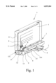
FIG. 1 shows electronic device 1 for seating on mounting rail 2. Mounting rail 2 is a top hat rail. The electronic device 1, itself, has a housing 3 which is made of an insulating material, especially plastic. In housing 3 is a circuit board 4. Circuit board 4 is provided, in a conventional manner with printed conductors 5 and with electronic components which are not shown in detail and they form no part of this invention.
Furthermore, device 1 has a plurality of contact means 6. The number of contact means 6 corresponds, in this case, to the number of printed conductor connections 7. In the embodiment shown in FIG. 1, there are five contact means 6. Contact means 6 are used, on the one hand, for making contact with circuit board 4, and on the other hand, for a data and/or power bus connection with adjacent devices 1 which have corresponding contact means 6 and which are seated on mounting rail 2. As follows especially from FIG. 4, each of contact means 6 has a circuit board contact 8, front bus contact 9 and rear bus contact 10.
Electronic devices 1 of the type described above can be placed in a row on mounting rail 2 based on their design, a data and/or power bus connection being formed via respective contact means 6.
In the embodiment shown in FIG. 1, it is now such that housing 3 is made in two parts; but, it is not necessary for this to be so. Housing 3 can also be made in one part. In the embodiment shown, housing 3 has an upper part 11 which holds circuit board 4 and a base part 12 which has the contact means 6. To make contact with circuit board 4, base part 12 has a circuit board receiver 13 which projects above the top side 14 of the base part 12. In circuit board receiver 13, there are circuit board contacts 8 of individual contact means 6. Front bus contacts 9, in the installed state, project from one longitudinal side 15 of base part 12. On the opposite longitudinal side (not shown), are rear bus contacts 10.
For detachable connection of the upper part 11 to the base part 12, a catch connection 15a is used. For detachable connection of base part 12 to mounting rail 2 a detachable lock is used which takes effect when base part 12 is swung onto mounting rail 2. For this reason on base part 12, there is a spring-loaded bolt 15b which is used for fitting under mounting rail 2 on one side when base part 12 is swung onto mounting rail 2.
It should be pointed out again that the embodiment shown in FIG. 1 is simply one embodiment of the invention. In particular, it is not necessary to make the housing 3 in two parts, i.e., with the upper part 11 and base part 12.
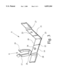
It is significant for this invention that circuit board contact 8, front bus contact 9 and rear bus contact 10 are composed of a continuous piece of flat, electrically conductive material. This is especially apparent from FIG. 2 in which an intermediate stage of production is shown. Circuit board contact 8, in the embodiment shown, is made as a so-called tulip-shaped contact receiver. For this reason, it has two contact legs 16, 17 which open outwardly. It follows especially from FIG. 1 that the circuit board contact 8 is aligned such that circuit board 4 is located roughly transversely to longitudinal direction L of the mounting rail.
As is apparent from FIG. 4, the front bus contact 9 is made in the form of a contact blade and the rear bus contact 10 in the form of a contact receiver. The bus contacts 9, 10, themselves, are aligned parallel relative to the longitudinal direction L of the mounting rail in the housing 3 or base part 12. So that front bus contact 9 of an adjacent electronic device 1 can be easily inserted into the contact receiver of rear bus contact 10, the contact is outwardly flared, proceeding from its central longitudinal axis M. Conversely, the contact blade of the front bus contact 9 becomes narrower toward its two longitudinal edges 18, 19. This also facilitates insertion or swinging of the electronic device 1 for producing a data and/or power bus connection to adjacent devices.
As is especially apparent from examination of FIGS. 2, 3 and 4, bus contacts 9, 10 are produced by folding strip 20 (compare FIG. 2) with formation of two legs 21, 22. The two legs 21, 22 are separated from one another via a fold line 23. In doing so, the folded end of strip 20 forms the contact blade, i.e. front bus contact 9, while the opposite, open end of folded strip 20 forms the contact receiver of rear bus contact 10. Circuit board contact 8 is located on longitudinal edge 18 of strip 20 or leg 22. The connection to strip 20 takes placed via bridge 24 which is bent such that it is located above leg 21.
In the folded-together state shown in FIG. 4, the two legs 21, 22 are securely joined to one another. For this reason, an opening 25 is provided in leg 21, while a projection 26 is provided on other leg 22. Projection 26 can be made in one part with strip 20 or leg 22 and can be produced, for example, by deep drawing, stamping, or plunge-cutting. Here, it can also be a separate part, for example, a rivet, in which case a corresponding opening is provided in leg 22. By riveting, fitting or welding of the projection 26, there is a form-fit and/or force-fit connection in opening 25.
Production of contact means 6 now proceeds as follows. From flat metal material, a continuous piece is produced, with first strip 20 and a second strip which runs parallel thereto (from which in the subsequent production stage circuit board contact 8 is formed) is punched out, the two strips being joined to one another via bridge 24. When the two strips are punched out, the opening 25 can be also be punched, and the projection 26 can be created as well. Then, each of the ends of the first strip 20 is bent to form a step 27, 28. The two angled ends which later form the contact receiver of rear bus contact 10 are slightly angled proceeding from the central longitudinal axis M, so that, in the folded state, the above described opening of rear bus contact 10 which flares outwardly results. Then, the strip 20 can be folded in the middle so that, on the folded end of the first strip 20, the contact blade of front bus contact 9 is formed, and on the back end, the contact receiver of rear bus contact 10 is formed.
In addition, the second strip is shaped to form the circuit board contact 8 such that the "tulip shape" with two contact legs 16, 17 which flare to the outside shown in FIGS. 2-4 is produced when the strip 20 is folded. The shaping or bending of circuit board contact 8 can, otherwise, also take place before the strip 20 is folded. Furthermore, it is still necessary to angle the second strip or circuit board contact 8 over bridge 24 relative to first strip 20, roughly at a right angle to the alignment of first strip 20.
Although the bridge 24 is shown to be located at the transition to the step 28, the bridge 24 can be located elsewhere on one of the two longitudinal edges 18, 19.
Strip 20 is chamfered between the two steps 27, 28 on longitudinal edges 18, 19 so that the contact blade of front bus contact 9 becomes narrower on its two longitudinal edges 18, 19 in the folded-together state (FIG. 4).
After the two legs 21, 22 are completely folded together, the projection 26 is fitted, riveted or welded in opening 25 so that a form-fit and/or force-fit connection arises between the two legs 21, 22.
As technically possible, the specific sequence of the individual process steps is optional; this means that the aforementioned process steps, if technically possible, can also have a sequence different that described above.
While only one embodiment in accordance with the present invention has been shown and described, it is understood that the invention is not limited thereto, and is susceptible to numerous changes and modifications as known to those skilled in the art. Therefore, this invention is not limited to the details shown and described herein, and includes all such changes and modifications as are encompassed by the scope of the appended claims.

Claims (9)

I claim:
1. An electrical or electronic device for seating on a mounting rail comprising a housing with at least one circuit board located in said housing and with at least one contact means having a circuit board contact for electrical connection with the circuit board, the circuit board contact having a contact receiver with two contact legs, and having a front bus contact and a rear bus contact for making one of a data and power bus connection with adjacent devices which have corresponding contact means; wherein the circuit board contact, the front bus contact and the rear bus contact are formed as part of a single continuous piece of electrically conductive sheet material having major surfaces and relatively thin edge surfaces, said sheet material having been punched and bent to form said contacts with the major and edge surfaces of portions of the sheet material from which the contact legs of the circuit board contact are formed being oriented crosswise relative to the major and edge surfaces of portions of the sheet material from which the front and rear bus contacts are formed.
2. The device as claimed in claim 1, wherein the circuit board is located roughly transversely to a longitudinal direction of a slot for axially receiving the mounting rail.
3. The device as claimed in claim 2, wherein a first of the front and rear bus contacts is a contact blade and a second of the bus contacts is contact receiver shaped for receiving a corresponding contact blade of said adjacent devices.
4. The device as claimed in claim 3, wherein the bus contacts are aligned parallel relative to said longitudinal direction of said slot.
5. The device as claimed in claim 3, wherein the contact receiver flares outwardly from a central longitudinal axis of the contact means.
6. The device as claimed in claim 3, wherein the contact blade has outwardly tapering longitudinal edges.
7. An electrical or electronic device for seating on a mounting rail comprising a housing with at least one circuit board located in said housing and with at least one contact means having a circuit board contact for electrical connection with the circuit board, the circuit board contact having a contact receiver with two contact legs, and having a front bus contact and a rear bus contact for making one of a data and power bus connection with adjacent devices which have corresponding contact means; wherein the circuit board contact, the front bus contact and the rear bus contact are formed as part of a single continuous piece of electrically conductive material; wherein a first of the front and rear bus contacts is a contact blade and a second of the front and rear bus contacts is a contact receiver; wherein the bus contacts are on opposite ends of a strip of said electrically conductive material which is folded in a manner forming a pair of legs connected by a fold, the contact blade being formed on a folded end of the strip, and the contact receiver being formed by outwardly bent free ends of the legs; and wherein the circuit board contact projects from a longitudinal edge of one of the legs.
8. The device as claimed in claim 7, wherein an opening is provided on one of said leg and a corresponding projection for fitting into said opening is provided on the other of said legs.
9. The device as claimed in claim 8, wherein said projection is held in said opening by one of a form-fit and a force-fit connection.
US09/073,644 1997-05-06 1998-05-06 Electrical or electronic device for seating on a mounting rail and process for producing same Expired - Lifetime US6033264A (en)

Applications Claiming Priority (2)

Application Number Priority Date Filing Date Title
DE19718996 1997-05-06
DE19718996A DE19718996C1 (en) 1997-05-06 1997-05-06 Module for rail mounted electronic module for data and energy bus lines

Publications (1)

Publication Number Publication Date
US6033264A true US6033264A (en) 2000-03-07

Family

ID=7828701

Family Applications (1)

Application Number Title Priority Date Filing Date
US09/073,644 Expired - Lifetime US6033264A (en) 1997-05-06 1998-05-06 Electrical or electronic device for seating on a mounting rail and process for producing same

Country Status (6)

Country Link
US (1) US6033264A (en)
EP (1) EP0877542B1 (en)
AT (1) ATE260018T1 (en)
DE (2) DE19718996C1 (en)
DK (1) DK0877542T3 (en)
ES (1) ES2213853T3 (en)

Cited By (11)

* Cited by examiner, † Cited by third party
Publication number Priority date Publication date Assignee Title
US6568943B2 (en) * 2000-10-18 2003-05-27 Sony Corporation Electric connection device, battery having electric connection device, and electronic equipment having battery
US6692311B1 (en) * 1999-10-25 2004-02-17 Omron Corporation Sensor system and connector used therefor
FR2912626A1 (en) * 2007-02-16 2008-08-22 Fernando Groisman Storage case for e.g. jewellery store, has electronic circuit including connector with male part that is inserted in female part of another connector of another case by electric connection for transmitting current towards circuit
FR2932316A1 (en) * 2008-06-09 2009-12-11 Hispano Suiza Sa Male-female connector for printed circuit boards in electronic control unit of e.g. airplane, has connection pins with three pairs of ends, where respective ends of pins form connection member to cross printed circuit board in mounted state
US20130027890A1 (en) * 2010-03-31 2013-01-31 Weidmueller Interface Gmbh & Co. Kg Connection module being capable of serving as a bus
JP2013526758A (en) * 2010-05-10 2013-06-24 ワイドミュラー インターフェース ゲゼルシャフト ミット ベシュレンクテル ハフツング ウント コンパニー コマンディートゲゼルシャフト Mounting rail bus system
DE102012204026A1 (en) 2012-03-14 2013-09-19 Dinkle Enterprise Co., Ltd. Data bus structure for coupling terminal blocks utilized to couple e.g. power lines, of processing machine, has two conductive elements insertable into slots of main body to form guide rail, where main body is plugable into supporting rail
US9078368B2 (en) 2011-08-24 2015-07-07 Phoenix Contact Gmbh & Co. Kg Cross-jump supporting I/O module and electrical contact element
US9548552B2 (en) 2011-05-13 2017-01-17 Te Connectivity Germany Gmbh Plug contact modules and plug contact arrangement for transmitting frequencies in the gigahertz range
US9583849B1 (en) * 2015-09-16 2017-02-28 Dinkle Enterprise Co., Ltd. Connector module with multiple connection modes
CN107425345A (en) * 2016-04-28 2017-12-01 町洋企业股份有限公司 Connector module and knife switch thereof

Families Citing this family (12)

* Cited by examiner, † Cited by third party
Publication number Priority date Publication date Assignee Title
DE19826390C2 (en) * 1998-06-12 2003-11-20 Whitaker Corp Electrical contact element
DE19851566A1 (en) * 1998-11-09 2000-05-11 Grote & Hartmann Potential distributor e.g. stackable connector strip for motor vehicle has locking elements to lock lug into receptacle
DE19856390A1 (en) * 1998-12-07 2000-06-08 Hoffmann Elektrokohle Electric motor noise suppression module e.g. for automobile electric fuel pump, has noise suppression circuit connected between input and output terminals supported by housing enclosing noise suppression circuit
DE29901194U1 (en) 1999-01-25 1999-05-20 Weidmueller Interface Bus conductor section for an electrical device
ATE233962T1 (en) * 1999-04-14 2003-03-15 Whitaker Corp ELECTRICAL CONNECTOR FOR AN INPUT/OUTPUT MODULE
DE29916302U1 (en) * 1999-09-16 2001-03-01 Weidmueller Interface Bus conductor section for an electrical device
DE10117061A1 (en) * 2001-04-05 2002-10-10 Delphi Tech Inc Electrical connector e.g. for high current equipment in motor vehicles, includes stack of mutually aligned contact elements forming at least one connection section
DE10227422B4 (en) 2002-06-20 2018-11-22 Werner Turck Gmbh & Co. Kg data converters
DE202010010275U1 (en) * 2010-07-15 2011-12-20 Weidmüller Interface GmbH & Co. KG Electrical contact part
BE1026797B1 (en) 2018-11-26 2020-06-22 Phoenix Contact Gmbh & Co Modular switching device for controlling at least one electric drive
LU102017B1 (en) * 2020-08-25 2022-02-25 Phoenix Contact Gmbh & Co potential distributor arrangement
DE102022109759A1 (en) 2022-04-22 2023-10-26 HARTING Electronics GmbH Bus connector for an electrical control system

Citations (9)

* Cited by examiner, † Cited by third party
Publication number Priority date Publication date Assignee Title
US4322120A (en) * 1980-05-19 1982-03-30 Hans Rilling Plug-in connector with improved spring contact
DE3215054A1 (en) * 1981-04-24 1982-11-11 La Télémécanique Electrique, 92002 Nanterre, Hauts-de-Seine SYSTEM FOR DISTRIBUTING PNEUMATIC CONTROL SIGNALS BY ELECTRICAL WAY
DE3436119A1 (en) * 1984-10-02 1986-04-03 Siemens AG, 1000 Berlin und 8000 München Contact spring element for making contact with printed circuit boards
EP0364618A1 (en) * 1988-10-18 1990-04-25 Weidmüller Interface GmbH & Co. Multiple signal transmission device
DE4140611C1 (en) * 1991-12-10 1993-05-27 Kloeckner-Moeller Gmbh, 5300 Bonn, De Bus contacting device for modular control system - comprises modular blocks with three-point contact for connecting bus board of module to contact surface of pcb surrounded by housing shell
DE4310369A1 (en) * 1993-03-30 1994-10-06 Amphenol Tuchel Elect adapter
DE4324061A1 (en) * 1993-07-17 1995-01-19 Weidmueller Interface Distribution strip
DE29514711U1 (en) * 1995-09-13 1995-11-02 Weidmueller Interface Terminal block arrangement
US5716241A (en) * 1994-01-18 1998-02-10 Wago Verwaltungsgesellschaft Mbh I/O device for a data bus

Family Cites Families (3)

* Cited by examiner, † Cited by third party
Publication number Priority date Publication date Assignee Title
US4331370A (en) * 1980-04-28 1982-05-25 Amp Incorporated Connection system for printed circuit boards
FR2559335B1 (en) * 1984-02-08 1986-05-23 Telemecanique Electrique MODULAR CELL FOR SUPPORTING AND PROTECTING ELECTRONIC CARDS
DE3614689A1 (en) * 1986-04-30 1987-11-05 Siemens Ag Arrangement of electrical assemblies of different formats

Patent Citations (9)

* Cited by examiner, † Cited by third party
Publication number Priority date Publication date Assignee Title
US4322120A (en) * 1980-05-19 1982-03-30 Hans Rilling Plug-in connector with improved spring contact
DE3215054A1 (en) * 1981-04-24 1982-11-11 La Télémécanique Electrique, 92002 Nanterre, Hauts-de-Seine SYSTEM FOR DISTRIBUTING PNEUMATIC CONTROL SIGNALS BY ELECTRICAL WAY
DE3436119A1 (en) * 1984-10-02 1986-04-03 Siemens AG, 1000 Berlin und 8000 München Contact spring element for making contact with printed circuit boards
EP0364618A1 (en) * 1988-10-18 1990-04-25 Weidmüller Interface GmbH & Co. Multiple signal transmission device
DE4140611C1 (en) * 1991-12-10 1993-05-27 Kloeckner-Moeller Gmbh, 5300 Bonn, De Bus contacting device for modular control system - comprises modular blocks with three-point contact for connecting bus board of module to contact surface of pcb surrounded by housing shell
DE4310369A1 (en) * 1993-03-30 1994-10-06 Amphenol Tuchel Elect adapter
DE4324061A1 (en) * 1993-07-17 1995-01-19 Weidmueller Interface Distribution strip
US5716241A (en) * 1994-01-18 1998-02-10 Wago Verwaltungsgesellschaft Mbh I/O device for a data bus
DE29514711U1 (en) * 1995-09-13 1995-11-02 Weidmueller Interface Terminal block arrangement

Cited By (16)

* Cited by examiner, † Cited by third party
Publication number Priority date Publication date Assignee Title
US6692311B1 (en) * 1999-10-25 2004-02-17 Omron Corporation Sensor system and connector used therefor
US20040142602A1 (en) * 1999-10-25 2004-07-22 Omron Corporation Sensor system and connector used therefor
US6945828B2 (en) 1999-10-25 2005-09-20 Omron Corporation Sensor system and connector used therefor
US6568943B2 (en) * 2000-10-18 2003-05-27 Sony Corporation Electric connection device, battery having electric connection device, and electronic equipment having battery
FR2912626A1 (en) * 2007-02-16 2008-08-22 Fernando Groisman Storage case for e.g. jewellery store, has electronic circuit including connector with male part that is inserted in female part of another connector of another case by electric connection for transmitting current towards circuit
FR2932316A1 (en) * 2008-06-09 2009-12-11 Hispano Suiza Sa Male-female connector for printed circuit boards in electronic control unit of e.g. airplane, has connection pins with three pairs of ends, where respective ends of pins form connection member to cross printed circuit board in mounted state
US20130027890A1 (en) * 2010-03-31 2013-01-31 Weidmueller Interface Gmbh & Co. Kg Connection module being capable of serving as a bus
US8986033B2 (en) * 2010-03-31 2015-03-24 Weidmueller Interface Gmbh & Co. Kg Connection module being capable of serving as a bus
JP2013526758A (en) * 2010-05-10 2013-06-24 ワイドミュラー インターフェース ゲゼルシャフト ミット ベシュレンクテル ハフツング ウント コンパニー コマンディートゲゼルシャフト Mounting rail bus system
US9548552B2 (en) 2011-05-13 2017-01-17 Te Connectivity Germany Gmbh Plug contact modules and plug contact arrangement for transmitting frequencies in the gigahertz range
US9078368B2 (en) 2011-08-24 2015-07-07 Phoenix Contact Gmbh & Co. Kg Cross-jump supporting I/O module and electrical contact element
DE102012204026A1 (en) 2012-03-14 2013-09-19 Dinkle Enterprise Co., Ltd. Data bus structure for coupling terminal blocks utilized to couple e.g. power lines, of processing machine, has two conductive elements insertable into slots of main body to form guide rail, where main body is plugable into supporting rail
US9583849B1 (en) * 2015-09-16 2017-02-28 Dinkle Enterprise Co., Ltd. Connector module with multiple connection modes
CN107425345A (en) * 2016-04-28 2017-12-01 町洋企业股份有限公司 Connector module and knife switch thereof
CN107425345B (en) * 2016-04-28 2019-11-15 町洋企业股份有限公司 Connector module and knife switch thereof
CN110635315A (en) * 2016-04-28 2019-12-31 町洋企业股份有限公司 Connector module and knife switch thereof

Also Published As

Publication number Publication date
ATE260018T1 (en) 2004-03-15
DE19718996C1 (en) 1998-06-04
ES2213853T3 (en) 2004-09-01
EP0877542A1 (en) 1998-11-11
DK0877542T3 (en) 2004-06-28
EP0877542B1 (en) 2004-02-18
DE59810773D1 (en) 2004-03-25

Similar Documents

Publication Publication Date Title
US6033264A (en) Electrical or electronic device for seating on a mounting rail and process for producing same
JP4011920B2 (en) Manufacturing method of connection terminal
EP0703117B1 (en) Electric connection casing
US5078625A (en) Wedge base socket attached to spg substrate
US5679034A (en) Construction of retaining resilient contact piece in female electrical connection member
US2904771A (en) Electrical connector with doubleended socket contacts
EP1372220B1 (en) A circuit board terminal
US7976345B2 (en) Electrical contact assembly and method of manufacturing thereof
US3955877A (en) Low profile contact
JPH05144484A (en) Insulation rejecting type probe and connector using this probe
JPH0636818A (en) Electric contact and electric connector using this
GB2058485A (en) Electrical terminals
US6238252B1 (en) Flat plug-in contact member for electrical plug-in connections
US4331376A (en) Electric connectors
US4017135A (en) Electrical contact element
US20010039139A1 (en) Insulation-displacement terminal contact, and a connecting terminal
EP0971461B1 (en) Electrical busbar with female terminals
US6848955B2 (en) Method for producing male terminal fittings and terminal fitting
US6241564B1 (en) Carrier plate for forming a plug contact
US10847913B2 (en) Terminal fitting
US6589084B1 (en) Device for plug-connecting electric lines
US6287158B1 (en) Contact element
US5332395A (en) Computer cable connectors
JP3226211B2 (en) Busbar wiring board
US5933946A (en) Process for providing an electronic module with a cover and terminal pins

Legal Events

Date Code Title Description
AS Assignment

Owner name: PHOENIX CONTACT GMBH & CO., GERMANY

Free format text: ASSIGNMENT OF ASSIGNORS INTEREST;ASSIGNOR:FEYE-HOHMANN, JURGEM;REEL/FRAME:009166/0395

Effective date: 19980429

AS Assignment

Owner name: PHOENIX CONTACT GMBH & CO., GERMANY

Free format text: ASSIGNMENT OF ASSIGNORS INTEREST;ASSIGNOR:FEYE-HOHMANN, JURGEN;REEL/FRAME:010207/0963

Effective date: 19980429

STCF Information on status: patent grant

Free format text: PATENTED CASE

FPAY Fee payment

Year of fee payment: 4

FEPP Fee payment procedure

Free format text: PAYOR NUMBER ASSIGNED (ORIGINAL EVENT CODE: ASPN); ENTITY STATUS OF PATENT OWNER: LARGE ENTITY

Free format text: PAYER NUMBER DE-ASSIGNED (ORIGINAL EVENT CODE: RMPN); ENTITY STATUS OF PATENT OWNER: LARGE ENTITY

FPAY Fee payment

Year of fee payment: 8

FPAY Fee payment

Year of fee payment: 12