US6028641A - Device and method for generating a stable system clock in HDTV - Google Patents
Device and method for generating a stable system clock in HDTV Download PDFInfo
- Publication number
- US6028641A US6028641A US08/862,963 US86296397A US6028641A US 6028641 A US6028641 A US 6028641A US 86296397 A US86296397 A US 86296397A US 6028641 A US6028641 A US 6028641A
- Authority
- US
- United States
- Prior art keywords
- signal
- clock
- signals
- selecting
- frame rate
- Prior art date
- Legal status (The legal status is an assumption and is not a legal conclusion. Google has not performed a legal analysis and makes no representation as to the accuracy of the status listed.)
- Expired - Fee Related
Links
Images
Classifications
-
- H—ELECTRICITY
- H04—ELECTRIC COMMUNICATION TECHNIQUE
- H04N—PICTORIAL COMMUNICATION, e.g. TELEVISION
- H04N5/00—Details of television systems
- H04N5/44—Receiver circuitry for the reception of television signals according to analogue transmission standards
- H04N5/46—Receiver circuitry for the reception of television signals according to analogue transmission standards for receiving on more than one standard at will
-
- H—ELECTRICITY
- H04—ELECTRIC COMMUNICATION TECHNIQUE
- H04N—PICTORIAL COMMUNICATION, e.g. TELEVISION
- H04N7/00—Television systems
- H04N7/015—High-definition television systems
-
- H—ELECTRICITY
- H04—ELECTRIC COMMUNICATION TECHNIQUE
- H04N—PICTORIAL COMMUNICATION, e.g. TELEVISION
- H04N21/00—Selective content distribution, e.g. interactive television or video on demand [VOD]
- H04N21/40—Client devices specifically adapted for the reception of or interaction with content, e.g. set-top-box [STB]; Operations thereof
- H04N21/41—Structure of client; Structure of client peripherals
- H04N21/426—Internal components of the client ; Characteristics thereof
-
- H—ELECTRICITY
- H04—ELECTRIC COMMUNICATION TECHNIQUE
- H04N—PICTORIAL COMMUNICATION, e.g. TELEVISION
- H04N21/00—Selective content distribution, e.g. interactive television or video on demand [VOD]
- H04N21/40—Client devices specifically adapted for the reception of or interaction with content, e.g. set-top-box [STB]; Operations thereof
- H04N21/43—Processing of content or additional data, e.g. demultiplexing additional data from a digital video stream; Elementary client operations, e.g. monitoring of home network or synchronising decoder's clock; Client middleware
- H04N21/4302—Content synchronisation processes, e.g. decoder synchronisation
- H04N21/4305—Synchronising client clock from received content stream, e.g. locking decoder clock with encoder clock, extraction of the PCR packets
Definitions
- the present invention relates to a digital TV receiver such as an HDTV(High Definition Television) receiver, and more particularly, to a device and method for generating a clock in an HDTV receiver.
- a digital TV receiver such as an HDTV(High Definition Television) receiver
- the GA video standard accommodates many kinds of video formats, and is not limited to a single video format.
- the GA format can accommodate video transmissions from various sources.
- the transmitter can transmit video signals at a mix of 59.9 Hz and 60 Hz video frame rates(or display rates) in 27 MHz reference frequency.
- display clock signals should be changed to match the transmitted 59.9 Hz or 60 Hz video frame rates.
- the receiver side is required to have clock signals of different sampling frequencies for the different video formats, each of those clock signals should be in agreement with the clock signal used on the transmitter side, i.e., in the encoder, or their line frequencies or field or frame frequencies should be in agreement, exactly.
- all digital television sets require a device for restoring clock signals without fail, which can appropriately change the present clock signal into a clock signal in agreement with the display format. If the restoration of the clock signal is not perfect, an overall picture quality will be degraded.
- a conventional HDTV clock generating device restores the clock signal transmitted from the transmitter by way of time restoration in which the receiver at first restores the transmitted data loaded on a carrier according to each of the video formats transmitted from the transmitter. And, a restored clock signal is passed through a PLL(Phase Locked Loop) to generate a desired frequency.
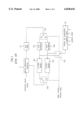
- a conventional clock generating device in an HDTV receiver includes local oscillators 13a and 13b for respectively generating clock signals of different frequencies, a 1/1000 frequency divider 14a for dividing the frequency of the clock signal from the local oscillator 13a by 1/1000, a 1/1001 frequency divider 14b for dividing the frequency of the clock signal from the local oscillator 13b by 1/1001, a phase error detector 11 for receiving a reference clock signal and the clock signal 1/1000 or 1/1001 divided of the clock signals from the local oscillator 13a and 13b and comparing the clock signals with the reference clock signals to detect a phase error signal, a loop filter 12 for converting the phase error signal from the phase error detector 11 into a signal voltage for controlling the local oscillators 13a and 13b, a first selector 15a for selecting one from the local oscillators 13a and 13b in providing the control signal from the loop filter 12 depending on a video format of a received video signal,
- the local oscillator 13a If the frame rate of the conventional clock generating device in an HDTV receiver is 59.9 Hz, the local oscillator 13a generates a frequency signal of 4788 fH when the sampling frequency is 4788 fH, which is 1/1000 divided in the 1/1000 divider 14a to generate a frequency signal of 4.788 fH, identical to the reference clock signal.
- the local oscillator 13b generates a clock signal of 4788 ⁇ (1001/1000), which is then 1/1001 divided in the 1/1001 divider 14b also to generate a frequency signal of 4.788 fh, identical to the reference clock signal, too.
- the selector 15c is used in selecting one clock signal from the two clock signals of the two local oscillators 13a and 13b depending on the video format of the received video signal. That is, when the video format of the received video signal has a frame rate of 59.94 Hz or 29.97 Hz, the selector 15c selects a signal from the local oscillator 13a, and when the video format of the received video signal has a frame rate of 30 Hz or 60 Hz, the selector 15c selects a signal from the local oscillator 13b.
- This selected clock signal can be used as a system clock signal after being demultiplied by the divider for system clock generating 16.
- the conventional clock generating device in an HDTV receiver selectively restores a clock signal corresponding to a video format of a received video signal.
- the conventional clock generating device selects a suitable clock signal from the PLL circuit by switching between the local oscillators and dividers in the PLL and uses the selected clock signal as a system clock signal.
- the conventional clock generating device in an HDTV receiver has a problem in that the clock signal becomes unstable when the switch in the PLL is changed over.
- the present invention is directed to a device and method for generating a clock signal in an HDTV receiver that substantially obviates one or more of the problems due to limitations and disadvantages of the related art.
- One object of the present invention is to provide a device for generating a clock in an HDTV receiver, which can make a stable change and provision of a system clock signal even when a format of a received video signal is changed.
- Another object of the present invention is to provide a device and method for generating a clock in an HDTV receiver, which can generate a system clock signal corresponding to a frame rate of a presently received video signal at a time when a frame rate of a just prior received video signal and the frame rate of the presently received video signal come to an agreement if the frame rates of these two video signals are different.
- the device for generating a clock in an HDTV receiver includes a clock generating part for generating a plurality of clock signals and selecting one clock signal from the clock signals in agreement to a frame rate of a presently received video signal having a reference clock signal in response to a provided clock selecting signal, and a controlling part for providing the clock selecting signal at a time when phases of the selected one clock signal of just prior video signal and the reference clock signal of the presently received video signal are in agreement to each other.
- a method for generating a clock in an HDTV including the steps of determining a frame rate of a presently received video signal having a reference clock signal and a frame rate of a just prior received video signal of being in agreement, detecting a time when phases of a display clock signal of the just prior video signal and the reference clock signal of the present video signal are in agreement to each other, if the two signals are different from each other, and generating a new clock signal suitable for displaying the presently received video signal from the time of detection.
- FIG. 1 illustrates a block diagram showing a system of a conventional device for generating a clock in an HDTV receiver
- FIG. 2 illustrates a block diagram showing an outline of a system of a device for generating a clock in an HDTV receiver in accordance with a preferred embodiment of the present invention
- FIG. 3 illustrates a block diagram showing a detailed system of the device for generating a clock in an HDTV receiver in FIG. 2;
- FIG. 4 illustrates a block diagram showing a detailed system of the device for generating a clock in an HDTV receiver in FIG. 3;
- FIG. 5 illustrates a block diagram showing a detailed circuit of a part of the device for generating a clock in an HDTV receiver in FIG. 4;
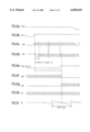
- FIGS. 6a ⁇ 6i illustrates timings for explaining the operation of the circuit shown in FIG. 5.
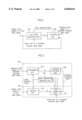
- FIG. 2 illustrates a block diagram showing an outline of a system for generating a clock in an HDTV receiver in accordance with a preferred embodiment of the present invention
- FIG. 3 illustrates a block diagram showing a detailed system for generating a clock in an HDTV receiver in FIG. 2
- FIG. 4 illustrates a block diagram showing a detailed system for generating a clock in an HDTV receiver in FIG. 3
- FIG. 5 illustrates a block diagram showing a detailed circuit of a part of the device for generating a clock in an HDTV receiver in FIG. 4.
- the device for generating a clock in an HDTV receiver includes a clock signal generating part 100 for generating a plurality of clock signals and selecting one clock signal from the clock signals in agreement with a frame rate of a received video signal having a reference clock signal in response to a clock selecting signal, and a controlling part 200 for receiving the selected clock signal of a prior video signal and the reference clock signal of the presently received video signal and providing the clock selecting signal at a time when phases of the two received clock signals are matched to each other using the plurality of clock signals.
- the reference clock signal has a 27 MHz frequency
- the frame rates of the received video signals are 59.94 Hz and 60 Hz.
- the video signals may include more than two frame rates.
- the display clock signal of the presently received video signal is generated from a low section of the clock signal coming next to the time when phases of the reference clock signal and the clock signal of the prior video signal are in agreement to each other.
- the clock signal generating part 100 generates a plurality of clock signals and selects one clock signal from the clock signals in response to a clock selecting signal from the controlling part 200 and provides the selected clock signal to a display part(not shown) as a display clock signal of a presently received video signal.
- the controlling part 200 determines a frame rate of the presently received video signal and a frame rate of the prior received video signal of being different from each other according to a reference clock signal of the presently received video signal and the display clock signal of the prior video signal, and then, if the frame rates of the two video signals are different from each other, detects a time when phases of the reference clock signal of the presently received video signal and the display clock signal of the prior video signal are in agreement to each other.
- the controlling part 200 When detected, the controlling part 200 provides a clock selecting signal to the clock signal generating part 100, and the clock signal generating part 100 provides one of the plurality of clock signals suitable for display of the presently received video signal. Though not shown in FIG. 2, the display displays the presently received video signal using this new display clock signal.
- the device for generating a clock includes a local oscillating part 101 for generating frequency signals corresponding to a plurality kind of video signals having frame rates different from one another received at an HDTV receiver in response to a provided oscillating control signal, a selecting part 102 for selecting one frequency signal from the frequency signals as the display clock signal in response to the provided clock selecting signal, a dividing part 201 for dividing the reference clock signal of the presently received video signal by a first dividing rate and the display clock signal from the selecting part 102 by a second dividing rate to provide a first divided signal and a second divided signal, an oscillation controlling part 202 for detecting a phase difference between the first divided signal and the second divided signal and providing an oscillation controlling signal corresponding to the phase difference to the oscillating part 101, and a phase location detecting part 203 for providing the clock selecting signal at a time when phases of the plurality kind of frequency signals come to an agreement.
- a local oscillating part 101 for generating frequency signals corresponding to a plurality kind of video signals having
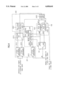
- the dividing part 201 in FIG. 3 includes a first divider 2011 for 1/1000 dividing the reference clock signal of the clock signal of the presently received video signal, a second divider 2012 for 1/1001 dividing the reference clock signal, a third divider 2013 for 1/2750 dividing the display clock signal from the selecting part 101 to provide the second divided signal, and a switching part 2014 for providing one of the signals from the first divider 2011 and the second divider 2012 as the first divided signal to the oscillation controlling part 202.
- the oscillation controlling part 202 shown in FIG. 3 includes a first phase difference detecting part 2021 for detecting a phase difference of the first divided signal and the second divided signal, and a loop filter part 2022 for providing a oscillation controlling signal corresponding to the phase difference.
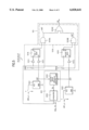
- the local oscillating part 102 shown in FIG. 3 includes at least two local oscillators. As shown in FIG. 4, the local oscillating part 102 shown in FIG. 3 includes a first local oscillator 1021 for providing a 74.25 MHz frequency signal in response to the oscillation controlling signal and the frame rate signal of a provided video signal, and a second local oscillator 1022 for providing a 74.176 MHz frequency signal in response to the signals. And, referring to FIG. 5, the phase agreement detecting part 203 shown in FIG.
- first inverter 1011 for inverting a first frequency signal of the plurality of frequency signals
- second inverter 1012 for inverting a second frequency signal of the plurality of frequency signals
- third inverter 1013 for inverting the clock selecting signal
- first latch 1014 for latching an output of the third inverter 1013 according to an output of the first inverter 1011
- second latch 1015 for latching the clock selecting signal according to an output of the second inverter 1012
- a multiplexer 1016 for selecting one from the first frequency signal and the second frequency signal in response to the outputs of the first, and second latches 1014 and 1015.
- the multiplexer 1016 includes a first AND gate 1016A for receiving the first frequency signal and a signal from the first latch 1014, a second AND gate 1016B for receiving the second frequency signal and a signal from the second latch 1015, and an OR gate 1016C for receiving signals from the first, and second AND gates 1016A and 1016B and providing the clock selecting signal.
- each of the first, and second latches 1014 and 1015 may includes a D type flipflop.
- a display clock signal is generated from a 27 MHz reference clock signal restored from a video signal transmitted from a transmitter through a transport decoder using the PLL.
- the reference clock signal is 1/1000 divided in the 1/1000 divider 2011 into a 27 KHz frequency signal, and 1/1001 divided in the 1/1001 divider 2012 into a 26.96 KHz frequency signal.
- One of the signals from the 1/1000 divider 2011 and the 1/1001 divider 2012 is selected by a control signal from the phase agreement detecting part 203, i.e, a clock selecting signal and provided to the first phase difference detecting part 2021.
- the phase difference detecting part 2021 detects a phase difference of the clock signals from the switching part 2014 and the third divider (1/2750 divider) 2013 and provides to the loop filter part 2022 which provides an oscillation control signal to the first, and second local oscillators 1021 and 1022.
- the first, and second local oscillators 1021 and 1022 receive a signal clk0 -- p and clk1 -- p(see FIGS.
- the second phase difference detecting part 2031 detects a difference of phases Ep(see FIG. 6i) of the signals clk0 and clk1 and provides to the comparing part 2032, and the comparing part 2032 provides a display clock selecting signal disp -- clk -- sel(see FIG. 6e) to the switching part 2014 and the selecting part 101 according to the phase difference.
- Each of the first, and second D type latches 1014 and 1015 in the selecting part 101 is provided with the clock selecting signal inverted in the third inverter 1013 at a D terminal thereof.
- the clock signals clkO and clkl from the first, and second local oscillators 1021 and 1022 respectively are inverted in the first, and second inverters 1011 and 1012 and provided to the first, and second D type latches 1014 and 1015 respectively at CP terminals thereof.
- Signals from the first, and second D type latches 1014 and 1015 and signals from the first, and second local oscillators 1021 and 1022 are received to the multiplexer 1016, and the multiplexer 1016 selects the clock signal from the first local oscillator 1021 when the clock selecting signal is "0" and the clock signal from the second local oscillator 1022 when the clock selecting signal is "1". That is, when a video format of a received video signal is changed from 59.94 Hz to 60 Hz or vice versa, the phase difference detecting part 203 detects the phase difference of the two clock signals from the first, and second local oscillators 1021 and 1022 and generates a clock selecting signal according to the phase difference.
- the selecting part 101 selects a clock signal from 74.25 MHz, and 74.176 MHz clock signals clk(see FIG. 6h) from the first, and second local oscillators 1021 and 1022 in response to the clock selecting signal.
- the clock signal from the selecting part 101 is provided to the third divider (1/2750 divider) 2013 and, on the same time, provided to the display part as a display clock signal.
- the display clock signal is changed according to a video format contained in a received video signal.
- the second phase detecting part 2031 in FIG. 5 detects a phase difference of a phase of the clock signal from each of the local oscillators and a phase of the reference clock signal and provides the display clock selecting signal disp -- clk -- sel when there is no phase difference.
- this display clock selecting signal disp -- clk -- sel causes to select a local oscillator which generates a clock signal in agreement to a video signal having another video format.
- the time when the display clock signal in agreement to the new video format is generated is in a low section of the clock signal coming next to the display clock selecting signal disp -- clk -- sel.
- the display clock signal clk1' in agreement to the new video format is generated in a low section of the clock signal coming next to the display clock selecting signal disp -- clk -- sel. It can be known from FIG. 6i that there is a portion in every 1000 clocks, in which the display clock signals of different formats of 59.94 Hz and 60 Hz are in agreement to each other.
- the device and method for generating a clock of the present invention is an implementation of device and method for generating a clock which can decode many kinds of video format.
- the device and method for generating a clock of the present invention detects a phase difference of two clock signals when video formats of received video signals are changed and changes over a switch from one format to another in low sections of following clock signals where there are no phase difference between the two clock signals. Accordingly, a stable supply of a display clock signal can be made possible in agreement to the presently received video signal.
Landscapes
- Engineering & Computer Science (AREA)
- Multimedia (AREA)
- Signal Processing (AREA)
- Synchronizing For Television (AREA)
- Television Systems (AREA)
Abstract
Description
Claims (20)
Applications Claiming Priority (2)
| Application Number | Priority Date | Filing Date | Title |
|---|---|---|---|
| KR96-19657 | 1996-06-03 | ||
| KR1019960019657A KR0172904B1 (en) | 1996-06-03 | 1996-06-03 | General clock generation apparatus of hdtv |
Publications (1)
| Publication Number | Publication Date |
|---|---|
| US6028641A true US6028641A (en) | 2000-02-22 |
Family
ID=19460692
Family Applications (1)
| Application Number | Title | Priority Date | Filing Date |
|---|---|---|---|
| US08/862,963 Expired - Fee Related US6028641A (en) | 1996-06-03 | 1997-06-03 | Device and method for generating a stable system clock in HDTV |
Country Status (2)
| Country | Link |
|---|---|
| US (1) | US6028641A (en) |
| KR (1) | KR0172904B1 (en) |
Cited By (14)
| Publication number | Priority date | Publication date | Assignee | Title |
|---|---|---|---|---|
| US6177959B1 (en) * | 1997-12-31 | 2001-01-23 | Telecruz Technology, Inc. | Circuit and method for generating a clock signal synchronized with time reference signals associated with television signals |
| EP1122953A2 (en) * | 2000-01-31 | 2001-08-08 | Nec Corporation | Image decoding device and method, storage medium and integrated circuit thereof |
| EP1152601A2 (en) * | 2000-05-02 | 2001-11-07 | Thomson Licensing S.A. | Horizontal synchronization for digital television receiver |
| EP0967798A3 (en) * | 1998-06-26 | 2002-01-09 | Sony Corporation | Video reproducing apparatus and reproducing method |
| WO2002032116A1 (en) * | 2000-10-11 | 2002-04-18 | Sony Electronics Inc. | Adaptive synchronization mechanism for digital video decoder |
| WO2002032148A1 (en) * | 2000-10-11 | 2002-04-18 | Sony Electronics Inc. | Adaptive clocking mechanism for digital video decoder |
| US20030174245A1 (en) * | 2002-03-12 | 2003-09-18 | Via Technologies, Inc. | Clock signal synthesizer with multiple frequency outputs and method for synthesizing clock signal |
| US20030174246A1 (en) * | 2002-03-12 | 2003-09-18 | Via Technologies, Inc. | Method and device for processing image data from non-interlacing type into interlacing one |
| US20030174247A1 (en) * | 2002-03-12 | 2003-09-18 | Via Technologies, Inc. | Adaptive deflicker method and adaptive deflicker filter |
| US6661846B1 (en) * | 1998-10-14 | 2003-12-09 | Sony Corporation | Adaptive clocking mechanism for digital video decoder |
| US20040205370A1 (en) * | 2003-04-09 | 2004-10-14 | International Business Machines Corporation | Method, apparatus and program storage device for providing clocks to multiple frequency domains using a single input clock of variable frequency |
| EP1665775A1 (en) * | 2003-09-22 | 2006-06-07 | Samsung Electronics Co., Ltd. | Display synchronization signal generation apparatus in digital broadcast receiver and decoder |
| US7268825B2 (en) * | 2003-04-01 | 2007-09-11 | Thomson Licensing Llc | Digital synchronizing generator |
| US20120206610A1 (en) * | 2011-02-11 | 2012-08-16 | Beibei Wang | Video quality monitoring |
Citations (1)
| Publication number | Priority date | Publication date | Assignee | Title |
|---|---|---|---|---|
| US4958228A (en) * | 1988-10-19 | 1990-09-18 | Matsushita Electric Industrial Co., Ltd. | Automatic frequency change device |
-
1996
- 1996-06-03 KR KR1019960019657A patent/KR0172904B1/en not_active IP Right Cessation
-
1997
- 1997-06-03 US US08/862,963 patent/US6028641A/en not_active Expired - Fee Related
Patent Citations (1)
| Publication number | Priority date | Publication date | Assignee | Title |
|---|---|---|---|---|
| US4958228A (en) * | 1988-10-19 | 1990-09-18 | Matsushita Electric Industrial Co., Ltd. | Automatic frequency change device |
Cited By (30)
| Publication number | Priority date | Publication date | Assignee | Title |
|---|---|---|---|---|
| US6177959B1 (en) * | 1997-12-31 | 2001-01-23 | Telecruz Technology, Inc. | Circuit and method for generating a clock signal synchronized with time reference signals associated with television signals |
| US7454124B2 (en) | 1998-06-26 | 2008-11-18 | Sony Corporation | Video reproducing apparatus and reproducing method |
| EP0967798A3 (en) * | 1998-06-26 | 2002-01-09 | Sony Corporation | Video reproducing apparatus and reproducing method |
| US7280744B2 (en) | 1998-06-26 | 2007-10-09 | Sony Corporation | Video reproducing apparatus and reproducing method |
| US20050158019A1 (en) * | 1998-06-26 | 2005-07-21 | Sony Corporation | Video reproducing apparatus and reproducing method |
| US20050152687A1 (en) * | 1998-06-26 | 2005-07-14 | Sony Corporation | Video reproducing apparatus and reproducing method |
| US6898371B1 (en) | 1998-06-26 | 2005-05-24 | Sony Corporation | Video reproducing apparatus and reproducing method |
| US20040047593A1 (en) * | 1998-10-14 | 2004-03-11 | Sony Corp | Adaptive clocking mechanism for digital video decoder |
| US7224736B2 (en) * | 1998-10-14 | 2007-05-29 | Sony Corporation | Adaptive clocking mechanism for digital video decoder |
| US6661846B1 (en) * | 1998-10-14 | 2003-12-09 | Sony Corporation | Adaptive clocking mechanism for digital video decoder |
| EP1122953A2 (en) * | 2000-01-31 | 2001-08-08 | Nec Corporation | Image decoding device and method, storage medium and integrated circuit thereof |
| EP1122953A3 (en) * | 2000-01-31 | 2005-03-09 | NEC Electronics Corporation | Image decoding device and method, storage medium and integrated circuit thereof |
| US6573944B1 (en) | 2000-05-02 | 2003-06-03 | Thomson Licensing S.A. | Horizontal synchronization for digital television receiver |
| EP1152601A3 (en) * | 2000-05-02 | 2003-03-26 | Thomson Licensing S.A. | Horizontal synchronization for digital television receiver |
| EP1152601A2 (en) * | 2000-05-02 | 2001-11-07 | Thomson Licensing S.A. | Horizontal synchronization for digital television receiver |
| WO2002032116A1 (en) * | 2000-10-11 | 2002-04-18 | Sony Electronics Inc. | Adaptive synchronization mechanism for digital video decoder |
| WO2002032148A1 (en) * | 2000-10-11 | 2002-04-18 | Sony Electronics Inc. | Adaptive clocking mechanism for digital video decoder |
| US20030174246A1 (en) * | 2002-03-12 | 2003-09-18 | Via Technologies, Inc. | Method and device for processing image data from non-interlacing type into interlacing one |
| US20030174247A1 (en) * | 2002-03-12 | 2003-09-18 | Via Technologies, Inc. | Adaptive deflicker method and adaptive deflicker filter |
| US7061537B2 (en) | 2002-03-12 | 2006-06-13 | Via Technologies, Inc. | Adaptive deflicker method and adaptive deflicker filter |
| US7084925B2 (en) | 2002-03-12 | 2006-08-01 | Via Technologies, Inc. | Method and device for processing image data from non-interlacing type into interlacing one |
| US7102690B2 (en) * | 2002-03-12 | 2006-09-05 | Via Technologies Inc. | Clock signal synthesizer with multiple frequency outputs and method for synthesizing clock signal |
| US20030174245A1 (en) * | 2002-03-12 | 2003-09-18 | Via Technologies, Inc. | Clock signal synthesizer with multiple frequency outputs and method for synthesizing clock signal |
| US7268825B2 (en) * | 2003-04-01 | 2007-09-11 | Thomson Licensing Llc | Digital synchronizing generator |
| US7171576B2 (en) | 2003-04-09 | 2007-01-30 | International Business Machines Corporation | Method, apparatus and program storage device for providing clocks to multiple frequency domains using a single input clock of variable frequency |
| US20040205370A1 (en) * | 2003-04-09 | 2004-10-14 | International Business Machines Corporation | Method, apparatus and program storage device for providing clocks to multiple frequency domains using a single input clock of variable frequency |
| EP1665775A4 (en) * | 2003-09-22 | 2008-06-18 | Samsung Electronics Co Ltd | Display synchronization signal generation apparatus in digital broadcast receiver and decoder |
| EP1665775A1 (en) * | 2003-09-22 | 2006-06-07 | Samsung Electronics Co., Ltd. | Display synchronization signal generation apparatus in digital broadcast receiver and decoder |
| US20120206610A1 (en) * | 2011-02-11 | 2012-08-16 | Beibei Wang | Video quality monitoring |
| US8885050B2 (en) * | 2011-02-11 | 2014-11-11 | Dialogic (Us) Inc. | Video quality monitoring |
Also Published As
| Publication number | Publication date |
|---|---|
| KR0172904B1 (en) | 1999-03-20 |
| KR980007645A (en) | 1998-03-30 |
Similar Documents
| Publication | Publication Date | Title |
|---|---|---|
| US6028641A (en) | Device and method for generating a stable system clock in HDTV | |
| JP3824172B2 (en) | PLL circuit | |
| US6704009B2 (en) | Image display | |
| KR100315246B1 (en) | Pll circuit for digital display device | |
| JP3520082B2 (en) | Display locked timing signal for video processing | |
| JP3654549B2 (en) | Circuit device for automatically recognizing the number of lines of a video synchronization signal | |
| US6449017B1 (en) | RGB self-alignment and intelligent clock recovery | |
| CN1068473C (en) | Phase detector for a phase-lock-loop | |
| WO1988006820A1 (en) | Receiver | |
| US6404833B1 (en) | Digital phase synchronizing apparatus | |
| JP2714327B2 (en) | Automatic tuning method and device | |
| FI105615B (en) | Digital method and apparatus for determining the frequency of an IF signal | |
| US7706490B2 (en) | Analog to digital converter clock synchronizer | |
| US6222590B1 (en) | Phase-locked loop circuit | |
| US7583802B2 (en) | Method for using a synchronous sampling design in a fixed-rate sampling mode | |
| US5315387A (en) | Horizontal synchronization circuit | |
| EP1205065B1 (en) | Method and apparatus for providing a clock signal with high frequency accuracy | |
| JP3353372B2 (en) | Liquid crystal display | |
| KR0135151B1 (en) | Clock generator for hdtv | |
| KR930011482B1 (en) | Phase synchronization loop circuit for digital video optical transmitting apparatus | |
| JP3257490B2 (en) | Synchronous protection circuit and method | |
| JPH05167989A (en) | High-definition television signal processing circuit | |
| KR20010028138A (en) | apparatus for correcting sync in digital TV | |
| JPH11112833A (en) | Horizontal synchronizing separator circuit | |
| JPS61234138A (en) | Phase locked loop |
Legal Events
| Date | Code | Title | Description |
|---|---|---|---|
| AS | Assignment |
Owner name: COUNTERBALANCE CORPORATION, PENNSYLVANIA Free format text: ASSIGNMENT OF ASSIGNORS INTEREST;ASSIGNOR:HOWARD, TIMOTHY L.;REEL/FRAME:008653/0087 Effective date: 19970603 |
|
| AS | Assignment |
Owner name: LG ELECTRONICS INC., KOREA, REPUBLIC OF Free format text: (ASSIGNMENT OF ASSIGNOR'S INTEREST) RE-RECORD TO CORRECT THE RECORDATION DATE OF 8-8-97 TO 8-5-97 ON A DOCUMENT PREVIOUSLY RECORDED AT REEL 8681 FRAME 484;ASSIGNOR:KIM, JIN-GYEONG;REEL/FRAME:008895/0666 Effective date: 19970531 |
|
| AS | Assignment |
Owner name: LG ELECTRONICS INC., KOREA, REPUBLIC OF Free format text: ;ASSIGNOR:KIM, JIN-GYEONG;REEL/FRAME:008681/0484 Effective date: 19970531 |
|
| FEPP | Fee payment procedure |
Free format text: PAYOR NUMBER ASSIGNED (ORIGINAL EVENT CODE: ASPN); ENTITY STATUS OF PATENT OWNER: LARGE ENTITY |
|
| FPAY | Fee payment |
Year of fee payment: 4 |
|
| FPAY | Fee payment |
Year of fee payment: 8 |
|
| FEPP | Fee payment procedure |
Free format text: PAYOR NUMBER ASSIGNED (ORIGINAL EVENT CODE: ASPN); ENTITY STATUS OF PATENT OWNER: LARGE ENTITY Free format text: PAYER NUMBER DE-ASSIGNED (ORIGINAL EVENT CODE: RMPN); ENTITY STATUS OF PATENT OWNER: LARGE ENTITY |
|
| REMI | Maintenance fee reminder mailed | ||
| LAPS | Lapse for failure to pay maintenance fees | ||
| STCH | Information on status: patent discontinuation |
Free format text: PATENT EXPIRED DUE TO NONPAYMENT OF MAINTENANCE FEES UNDER 37 CFR 1.362 |
|
| FP | Lapsed due to failure to pay maintenance fee |
Effective date: 20120222 |