US6013946A - Wire bond packages for semiconductor chips and related methods and assemblies - Google Patents
Wire bond packages for semiconductor chips and related methods and assemblies Download PDFInfo
- Publication number
- US6013946A US6013946A US08/831,465 US83146597A US6013946A US 6013946 A US6013946 A US 6013946A US 83146597 A US83146597 A US 83146597A US 6013946 A US6013946 A US 6013946A
- Authority
- US
- United States
- Prior art keywords
- dam
- insulating layer
- semiconductor chip
- input
- conductive traces
- Prior art date
- Legal status (The legal status is an assumption and is not a legal conclusion. Google has not performed a legal analysis and makes no representation as to the accuracy of the status listed.)
- Expired - Lifetime
Links
Images


Classifications
-
- H—ELECTRICITY
- H10—SEMICONDUCTOR DEVICES; ELECTRIC SOLID-STATE DEVICES NOT OTHERWISE PROVIDED FOR
- H10W—GENERIC PACKAGES, INTERCONNECTIONS, CONNECTORS OR OTHER CONSTRUCTIONAL DETAILS OF DEVICES COVERED BY CLASS H10
- H10W70/00—Package substrates; Interposers; Redistribution layers [RDL]
- H10W70/60—Insulating or insulated package substrates; Interposers; Redistribution layers
- H10W70/67—Insulating or insulated package substrates; Interposers; Redistribution layers characterised by their insulating layers or insulating parts
- H10W70/68—Shapes or dispositions thereof
-
- H—ELECTRICITY
- H10—SEMICONDUCTOR DEVICES; ELECTRIC SOLID-STATE DEVICES NOT OTHERWISE PROVIDED FOR
- H10W—GENERIC PACKAGES, INTERCONNECTIONS, CONNECTORS OR OTHER CONSTRUCTIONAL DETAILS OF DEVICES COVERED BY CLASS H10
- H10W74/00—Encapsulations, e.g. protective coatings
- H10W74/10—Encapsulations, e.g. protective coatings characterised by their shape or disposition
- H10W74/111—Encapsulations, e.g. protective coatings characterised by their shape or disposition the semiconductor body being completely enclosed
- H10W74/129—Encapsulations, e.g. protective coatings characterised by their shape or disposition the semiconductor body being completely enclosed forming a chip-scale package [CSP]
-
- H—ELECTRICITY
- H10—SEMICONDUCTOR DEVICES; ELECTRIC SOLID-STATE DEVICES NOT OTHERWISE PROVIDED FOR
- H10W—GENERIC PACKAGES, INTERCONNECTIONS, CONNECTORS OR OTHER CONSTRUCTIONAL DETAILS OF DEVICES COVERED BY CLASS H10
- H10W74/00—Encapsulations, e.g. protective coatings
- H10W74/10—Encapsulations, e.g. protective coatings characterised by their shape or disposition
- H10W74/111—Encapsulations, e.g. protective coatings characterised by their shape or disposition the semiconductor body being completely enclosed
- H10W74/114—Encapsulations, e.g. protective coatings characterised by their shape or disposition the semiconductor body being completely enclosed by a substrate and the encapsulations
- H10W74/117—Encapsulations, e.g. protective coatings characterised by their shape or disposition the semiconductor body being completely enclosed by a substrate and the encapsulations the substrate having spherical bumps for external connection
-
- H—ELECTRICITY
- H10—SEMICONDUCTOR DEVICES; ELECTRIC SOLID-STATE DEVICES NOT OTHERWISE PROVIDED FOR
- H10W—GENERIC PACKAGES, INTERCONNECTIONS, CONNECTORS OR OTHER CONSTRUCTIONAL DETAILS OF DEVICES COVERED BY CLASS H10
- H10W76/00—Containers; Fillings or auxiliary members therefor; Seals
- H10W76/40—Fillings or auxiliary members in containers, e.g. centering rings
- H10W76/42—Fillings
- H10W76/47—Solid or gel fillings
-
- H—ELECTRICITY
- H10—SEMICONDUCTOR DEVICES; ELECTRIC SOLID-STATE DEVICES NOT OTHERWISE PROVIDED FOR
- H10W—GENERIC PACKAGES, INTERCONNECTIONS, CONNECTORS OR OTHER CONSTRUCTIONAL DETAILS OF DEVICES COVERED BY CLASS H10
- H10W76/00—Containers; Fillings or auxiliary members therefor; Seals
- H10W76/60—Seals
-
- H—ELECTRICITY
- H10—SEMICONDUCTOR DEVICES; ELECTRIC SOLID-STATE DEVICES NOT OTHERWISE PROVIDED FOR
- H10W—GENERIC PACKAGES, INTERCONNECTIONS, CONNECTORS OR OTHER CONSTRUCTIONAL DETAILS OF DEVICES COVERED BY CLASS H10
- H10W90/00—Package configurations
- H10W90/701—Package configurations characterised by the relative positions of pads or connectors relative to package parts
- H10W90/751—Package configurations characterised by the relative positions of pads or connectors relative to package parts of bond wires
- H10W90/756—Package configurations characterised by the relative positions of pads or connectors relative to package parts of bond wires between a chip and a stacked lead frame, conducting package substrate or heat sink
-
- H—ELECTRICITY
- H10—SEMICONDUCTOR DEVICES; ELECTRIC SOLID-STATE DEVICES NOT OTHERWISE PROVIDED FOR
- H10W—GENERIC PACKAGES, INTERCONNECTIONS, CONNECTORS OR OTHER CONSTRUCTIONAL DETAILS OF DEVICES COVERED BY CLASS H10
- H10W95/00—Packaging processes not covered by the other groups of this subclass
-
- H—ELECTRICITY
- H10—SEMICONDUCTOR DEVICES; ELECTRIC SOLID-STATE DEVICES NOT OTHERWISE PROVIDED FOR
- H10W—GENERIC PACKAGES, INTERCONNECTIONS, CONNECTORS OR OTHER CONSTRUCTIONAL DETAILS OF DEVICES COVERED BY CLASS H10
- H10W72/00—Interconnections or connectors in packages
- H10W72/01—Manufacture or treatment
- H10W72/0198—Manufacture or treatment batch processes
-
- H—ELECTRICITY
- H10—SEMICONDUCTOR DEVICES; ELECTRIC SOLID-STATE DEVICES NOT OTHERWISE PROVIDED FOR
- H10W—GENERIC PACKAGES, INTERCONNECTIONS, CONNECTORS OR OTHER CONSTRUCTIONAL DETAILS OF DEVICES COVERED BY CLASS H10
- H10W72/00—Interconnections or connectors in packages
- H10W72/50—Bond wires
- H10W72/551—Materials of bond wires
- H10W72/552—Materials of bond wires comprising metals or metalloids, e.g. silver
- H10W72/5522—Materials of bond wires comprising metals or metalloids, e.g. silver comprising gold [Au]
-
- H—ELECTRICITY
- H10—SEMICONDUCTOR DEVICES; ELECTRIC SOLID-STATE DEVICES NOT OTHERWISE PROVIDED FOR
- H10W—GENERIC PACKAGES, INTERCONNECTIONS, CONNECTORS OR OTHER CONSTRUCTIONAL DETAILS OF DEVICES COVERED BY CLASS H10
- H10W72/00—Interconnections or connectors in packages
- H10W72/50—Bond wires
- H10W72/551—Materials of bond wires
- H10W72/552—Materials of bond wires comprising metals or metalloids, e.g. silver
- H10W72/5524—Materials of bond wires comprising metals or metalloids, e.g. silver comprising aluminium [Al]
-
- H—ELECTRICITY
- H10—SEMICONDUCTOR DEVICES; ELECTRIC SOLID-STATE DEVICES NOT OTHERWISE PROVIDED FOR
- H10W—GENERIC PACKAGES, INTERCONNECTIONS, CONNECTORS OR OTHER CONSTRUCTIONAL DETAILS OF DEVICES COVERED BY CLASS H10
- H10W72/00—Interconnections or connectors in packages
- H10W72/851—Dispositions of multiple connectors or interconnections
- H10W72/853—On the same surface
- H10W72/865—Die-attach connectors and bond wires
-
- H—ELECTRICITY
- H10—SEMICONDUCTOR DEVICES; ELECTRIC SOLID-STATE DEVICES NOT OTHERWISE PROVIDED FOR
- H10W—GENERIC PACKAGES, INTERCONNECTIONS, CONNECTORS OR OTHER CONSTRUCTIONAL DETAILS OF DEVICES COVERED BY CLASS H10
- H10W90/00—Package configurations
- H10W90/701—Package configurations characterised by the relative positions of pads or connectors relative to package parts
- H10W90/731—Package configurations characterised by the relative positions of pads or connectors relative to package parts of die-attach connectors
- H10W90/734—Package configurations characterised by the relative positions of pads or connectors relative to package parts of die-attach connectors between a chip and a stacked insulating package substrate, interposer or RDL
-
- H—ELECTRICITY
- H10—SEMICONDUCTOR DEVICES; ELECTRIC SOLID-STATE DEVICES NOT OTHERWISE PROVIDED FOR
- H10W—GENERIC PACKAGES, INTERCONNECTIONS, CONNECTORS OR OTHER CONSTRUCTIONAL DETAILS OF DEVICES COVERED BY CLASS H10
- H10W90/00—Package configurations
- H10W90/701—Package configurations characterised by the relative positions of pads or connectors relative to package parts
- H10W90/751—Package configurations characterised by the relative positions of pads or connectors relative to package parts of bond wires
- H10W90/754—Package configurations characterised by the relative positions of pads or connectors relative to package parts of bond wires between a chip and a stacked insulating package substrate, interposer or RDL
Definitions
- the present invention relates to the field of semiconductor chips and more particularly to assemblies, methods, and packages for semiconductor chips.
- the ball grid array (BGA) package provides a relatively high surface-mount density and improved electrical performance when compared with a conventional plastic package having a leadframe.
- a primary difference between a ball grid array package and a conventional plastic package is that the electrical connection between the semiconductor chip and the main board is provided by a substrate including multiple layers with circuit patterns instead of a leadframe of a plastic package.
- the semiconductor chip is attached and electrically connected to a substrate having vias which interconnect electrically conductive traces on the top layer of the substrate where the chip is attached to terminals on the bottom layer of the substrate opposite the chip.
- the terminals on the bottom layer of the substrate can be provided in an array pattern so that the area occupied by the BGA package on a main board is smaller than that of a conventional plastic package with peripheral terminals.
- the substrate used in the BGA package may still be larger than the semiconductor chip because an area without conductive traces may be required when attaching the chip to the substrate. Further reductions in the size of a BGA package may thus be limited. In response, further size reductions for semiconductor chip packages have been provided by chip-scale packages (CSP).
- CSP chip-scale packages
- the micro-BGA ⁇ BGA is a chip-scale package developed by Tessera and illustrated in FIG. 1. The micro-BGA is discussed in greater detail in the following reference: Crowley et al., "Chip Size Packaging Developments", TechSearch International, Inc., August 1995, pp. 101-109.
- the leads 57 are bonded with the chip pads 52 using a technique similar to tape automated bonding (TAB).
- TAB tape automated bonding
- the bonding area is encapsulated with a silicone encapsulant 59.
- the reduced size and inductance of the micro-BGA package 50 facilitate its use for packaging high speed semiconductor chips.
- the cost of manufacturing the micro-BGA package 50 may be relatively high as a result of the fabrication of the bumps 58 and the flexible circuit interposer 56.
- the alignment of the chip pads 52 with the leads 57 may be difficult when bonding the package.
- the tape automated bonding technique may be difficult to use with the micro-BGA package 50.
- a package for a semiconductor chip including a plurality of input/output pads on a surface thereof.
- a package according to the present invention includes an insulating layer with a first surface for bonding with the surface of the semiconductor chip so that the input/output pads are exposed adjacent the insulating layer.
- the package also includes a plurality of conductive traces on a second surface of the insulating layer opposite the first surface wherein each of the conductive traces corresponds to a respective one of the input/output pads.
- the conductive traces are adapted to receive a plurality of bonding wires each of which corresponds to a respective one of the input/output pads so that each of the bonding wires can be bonded at a first end to the respective input/output pad and at a second end to the respective conductive trace.
- the package can also include a plurality of terminals on the insulating layer outside the dam wherein each of the terminals is electrically connected to a respective one of the conductive traces. These terminals can be used to provide a connection between the package and a main board.
- each of the terminals preferably extends a first predetermined distance from the insulating layer
- the dam preferably extends a second predetermined distance from the insulating layer
- the first predetermined distance is preferably greater than the second predetermined distance. Accordingly, the package can be bonded with a main board using the terminals without creating any contacts between the dam and the main board.
- the dam can be a rectangular dam surrounding the opening. Accordingly, any encapsulant contained therein can be prevented from flowing across undesired portions of the insulating layer before hardening.
- at least one tie bar can extend from the dam, and a rail can be connected to the tie bar. More particularly, the dam, the at least one tie bar, and the rail can be formed from a single layer of material. The tie bar and the rail thus facilitate the continuous production of semiconductor chip assemblies wherein each of a plurality of assemblies includes a dam connected by tie bars to a common rail. After manufacture, the individual assemblies can be separated by breaking the tie bar away from the dam. In particular, a notch on the tie bar adjacent the dam can be used to facilitate the removal.
- the conductive traces are adapted to receive a plurality of bonding wires each of which corresponds to a respective one of the input/output pads so that each of the bonding wires can be bonded at a first end to the respective input/output pad and at a second end to the respective conductive trace.
- a method for packaging a semiconductor chip including a plurality of input/output pads on an interior portion of a surface thereof includes the step of forming an insulating layer including a first surface for bonding with the surface of the semiconductor chip wherein the insulating layer has an opening therein for exposing the input/output pads.
- a plurality of conductive traces are formed on a second surface of the insulating layer opposite the first surface wherein each of the conductive traces corresponds to a respective one of the input/output pads.
- a dam is formed on the second surface of the insulating layer around the opening wherein each of the conductive traces extends from adjacent the opening under the dam to a portion of the insulating layer outside the dam.
- the methods, packages, and assemblies of the present invention can thus be used to provide a semiconductor chip assembly with physical dimensions on the order of those of the semiconductor chip. Accordingly, a highly integrated semiconductor chip can be electrically and mechanically connected to a main board while occupying a relatively small surface area of the main board. The size of the package also reduces the inductance and resistance of the electrical connection with the main board thus improving the performance of the chip in terms of speed and power consumption.
- the wire bonds between the semiconductor chip and the package can also be cost effectively formed to provide a robust mechanical and electrical connection. Furthermore, the use of the dam can facilitate the protective encapsulation of the wire bonds.
- FIG. 1 is a cross-sectional view illustrating a chip package according to the prior art.
- FIG. 2 is a perspective view illustrating a first semiconductor chip assembly according to the present invention.
- FIGS. 4-10 are perspective views illustrating steps of a method for fabricating the semiconductor chip assembly of FIGS. 2 and 3.
- FIG. 11 is a perspective view illustrating a second semiconductor chip assembly according to the present invention.
- FIG. 12 is a cross-sectional view taken along section line 12--12 of FIG. 11.
- FIGS. 13-18 are perspective views illustrating steps of a method for fabricating the semiconductor chip assembly of FIGS. 11 and 12.
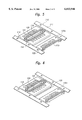
- FIG. 2 illustrates a chip-scale semiconductor chip assembly 100 according to the present invention
- FIG. 3 is a cross-sectional view taken along section lines 3--3 of FIG. 2.
- the assembly 100 includes both bonding wires 150 and terminals 170 on a surface of a circuit substrate 120a opposite a surface attached to the semiconductor chip 130.
- the semiconductor chip is attached to the surface of the circuit substrate 120a opposite the terminals 170 and conductive traces 121. Accordingly, the circuit substrate 120a can be reduced to a size on the order of that of the semiconductor chip. Furthermore, conventional vias are not required in the circuit substrate 120a.
- the circuit substrate 120a includes a top surface, a bottom surface, and an opening 123.
- the conductive traces 121 and the terminals 170 are formed on the top surface of the circuit substrate 120a.
- the conductive traces 121 can be used to route electrical signals to and from the semiconductor chip 130, and each trace 121 has a land pad 122 for mounting the respective terminal 170.
- the semiconductor chip 130 is attached to the bottom surface of the circuit substrate 120a, and the opening 123 extends through a central portion of the circuit substrate 120a to expose the input/output pads 131.
- a printed circuit board may be preferably used to provide the circuit substrate 120a of the present invention, other substrates can alternately be used.
- the circuit substrate 120a can be a glass substrate, a ceramic substrate, or a metallic substrate.
- the semiconductor chip 130 has a plurality of input/output pads 131 which are formed on a central or interior portion of the surface of the semiconductor chip 130.
- the semiconductor chip 130 is attached to the bottom surface of the circuit substrate 120a by a non-conductive adhesive 142. As shown, the input/output pads 131 are formed on the surface of the semiconductor chip which is affixed to the circuit substrate 120a. Accordingly, the input/output pads 131 are exposed through the opening 123 of the circuit substrate 120a.
- the input/output pads 131 and the conductive traces 121 are electrically connected by bonding wires through the opening 123 of the circuit substrate 120a.
- a portion of each conductive trace 121 extends to a portion of the circuit substrate adjacent the opening 123 where the wire bond connection is made.
- bonding wires 150 such as gold (Au) or aluminum (Al) bonding wires, are used to provide the wire bond.
- Au gold
- Al aluminum
- a dam 115 is attached to the top surface of the circuit substrate 120a using a non-conductive adhesive 141.
- the dam 115 can surround the opening 123 so that each conductive trace 121 extends from the wire bonding area adjacent the opening 123 under the dam 115 to a portion of the circuit substrate outside the dam 115 where a respective landing pad 122 is located.
- the dam 115 may have a rectangular ring shape with a predetermined height and a predetermined width.
- the space inside the dam 115 will be referred to as a window 116, and the window 116 is preferably larger than the opening 123 of the circuit substrate 120a. The wire bonding area of each conductive trace is thus exposed through the window 116.
- the dam 115 is preferably formed as an element of a strip including multiple dams, tie bars, and rails which allow the dams to be supported in a manner similar to that of a leadframe strip.
- the assemblies 100 can thus be continuously produced and mechanically supported during manufacture.
- the dam 115 also provides a structure which supports encapsulation of the bonding wires.
- the portion of the tie bar which remains after separating the assembly from the rails is designated by the reference number 113a of FIG. 2.
- the bonding wires 150, the input/output pads 131, and the portions of the conductive traces 121 exposed by the window 116 can be encapsulated by an encapsulant 161 such as a potting resin.
- the encapsulant can be contained within the opening 123 and the window 116.
- a liquid potting resin can protect the input/output pads 131, the bonding wires 150, and the portions of the conductive traces 121 within the window 116 from environmental contaminants.
- the dam 115 makes it possible to control the process of potting.
- the dam 115 prevents the potting resin 161 from overflowing, and the dam can be used to maintain a height of the potting resin at a desired level. In other words, the dam 115 can act as an index.
- the dam can prevent the potting resin from flowing across undesired portions of the surface of the circuit substrate 120a.
- these elements can be encapsulated with a sealing lid 162 as discussed below with regard to FIGS. 11 and 12.
- the terminals 170 are formed on the land pads 122 of the circuit substrate 120a.
- the terminals 170 are outer electrodes of the assembly 100 which permit external electrical connections between the semiconductor chip 130 and a main board.
- the height of the terminals 170 may be reduced. Accordingly, the terminals 170 should have a height greater than that of the dam 115 because the dam 115 should preferably not make contact with the main board.
- the terminals 170 have a height which is three times greater than that of the dam 115.
- each terminal 170 is 0.76 mm
- the height of each terminal 170 on the land pad 122 is about 0.6 mm
- the height of each terminal 170 once connected to a main board is about 0.4 mm.
- the dam 115 is thus preferably about 0.2 mm high and the height of a bonding wire above the circuit substrate is preferably 0.1 mm or less.
- FIGS. 4 through 10 illustrate steps of a method for forming the chip-scale assembly 100 of FIGS. 2 and 3.
- a dam carrier 110 is prepared.
- the dam carrier 110 is preferably formed as a continuous strip similar to a leadframe for a plastic package.
- the dam carrier 110 has two parallel guide rails 111 on opposite sides of each dam, and the dams 115 are linked to the guide rails 111 by tie bars 113.
- the dam carrier 110 can be made from a rigid material such as a metal, and the dam carrier can be formed using stamping or etching techniques.
- Guide holes 112 and the guide rails 111 facilitate continuous production.
- the tie bars 113 link the dams 115 to the guide rails 111, and the dams 115 preferably have a rectangular ring shape to define the window 116.
- Each tie bar 113 preferably has at least one notch 114 which aids in the separation of individual packages when the manufacturing steps have been completed.
- the semiconductor chip and the circuit substrate discussed above with regard to FIGS. 2 and 3 may be prepared separately.
- the circuit substrate 120a is attached to the dam 115 of the dam carrier 110.
- the circuit substrate 120a includes conductive traces 121 and land pads 122 which are formed on a top surface thereof.
- the circuit substrate also includes an opening 123 which extends through an interior portion of the circuit substrate 120a.
- the opening 123 is preferably smaller than the window 116 of the dam carrier 110. Portions of the conductive traces 121 are thus exposed through the window 116, and these exposed portions adjacent the opening can be used for wire bonding.
- the exposed portions of the conductive traces 121 adjacent the opening 123 can be connected with the semiconductor chip 130 as discussed below with regard to FIG. 7.
- the length of the long side of the circuit substrate 120a is preferably smaller than the distance between the two guide rails 111, and greater than the distance between the notches 114 which are provided at opposing sides of the dam 115.
- the notches 114 are thus positioned over the circuit substrate 120a preventing the remaining portion 113a of the tie bar from touching and affecting other devices when the package 100 is mounted on a main board.
- the adhesive 141 is an electrically non-conductive material.
- the step of attaching the integrated circuit chip 130 to the circuit substrate 120a is shown in FIG. 6.
- the semiconductor chip 130 is attached to the bottom surface of the circuit substrate 120a opposite the dam and the conductive traces.
- the semiconductor chip 130 has a plurality of chip pads 131 formed on an interior portion of the surface thereof.
- the chip pads 131 are thus exposed by the opening 123 of the circuit substrate, and an electrically non-conductive adhesive 142 is used to attach the semiconductor chip to the circuit substrate.
- the chip pads 131 are exposed to the opening 123, and wire bonding portions of the conductive traces 121 are exposed to the window 116 adjacent the opening 123.
- bonding wires can be used to connect the chip pads 131 and the conductive traces 121 as shown in FIG. 7.
- the bonding wires 150 can be gold or aluminum wires.
- the bonding wires 150 can be covered with an encapsulant 161 such as a potting resin as shown in FIG. 8.
- an encapsulant 161 such as a potting resin as shown in FIG. 8.
- a potting resin such as an epoxy resin similar to that used in a plastic package can be used.
- the encapsulant can be provided by screen printing or other techniques, and the dam 115 can prevent the potting resin from overflowing onto other portions of the circuit substrate 120a.
- the dam thus enables the potting resin to maintain a desired height below that of the dam 115.
- the dam enables the potting resin to be formed to a predetermined height above the bonding wires without spreading across the surface of the circuit substrate.
- the step of forming the terminals 170 on the circuit substrate 120a is illustrated in FIG. 9.
- the terminals 170 can be solder balls or other electrically conductive materials, and these terminals are formed on the land pads 122. Accordingly, the terminals 170 are physically and electrically connected with the land pads 122. In particular, the terminals 170 preferably have a height greater than that of solder dam 115. Solder balls may be formed using solder mounting or reflow methods known to those having skill in the art. Other electrically conductive materials used to form the terminals 170 can include Au/Sn, Cu/Au/Sn, or other similar layered structures, and these structures can be formed by metal plating or screen printing techniques.
- the dam carrier 110 allows the terminals 170 to be formed using conventional techniques. Alternately, the terminals can be formed on the circuit substrate prior to joining with the dam.
- the packages can then be separated into individual packages 100 as shown in FIG. 10.
- the separation can be achieved by cutting the tie bars 113 from the dam 115.
- the notch 114 on each tie bar 113 can facilitate separation.
- the notch 114 allows the separation to occur at the notch upon application of a relatively slight pressure.
- FIG. 11 illustrates a second semiconductor chip assembly 200 according to the present invention
- FIG. 12 is a cross-sectional view taken along section line 12--12 of FIG. 11. Because FIGS. 11 and 12 correspond to FIGS. 2 and 3, common elements are designated by common reference numbers. Accordingly, these common elements will not be discussed in detail, and the following discussion will relate primarily to the differences therebetween.
- the bonding wires are encapsulated with a sealing lid 162 which is mounted on the dam 115.
- the window 116 defined by the dam 115 is covered by the sealing lid 162.
- the top surface of the sealing lid 162 has a height after mounting that is less than the height of the terminals 170.
- the terminals are formed on the circuit substrate before attachment to the dam 115.
- the terminals were not formed until after assembling the semiconductor chip, the circuit substrate, and the dam.
- the terminals can be formed on the circuit substrate before or after assembly in either the method discussed with reference to FIGS. 3-10 or the method discussed with reference to FIGS. 13-18.
- FIGS. 13 through 18 illustrate steps of a method for forming the chip-scale semiconductor chip assembly 200 of FIGS. 11 and 12.
- the dam carrier 110 is prepared as shown in FIG. 13.
- the semiconductor chip and the circuit substrate can be simultaneously prepared.
- the circuit substrate 120b is attached to the dam 115 of the dam carrier 110 as shown in FIG. 14.
- the terminals 170 have been previously formed on the circuit substrate 120b. Alternately, the terminals 170 can be formed at later steps in the method such as after the bonding wires have been encapsulated.
- FIGS. 15 and 16 The steps of attaching the semiconductor chip 130 to the circuit substrate 120b and electrically connecting the semiconductor chip 130 to the circuit substrate 120b are illustrated in FIGS. 15 and 16.
- chip pads 131 are electrically connected to respective conductive traces 121 by bonding wires 150.
- the window 116 of the dam and the opening 123 of the circuit substrate are encapsulated with a sealing lid 162 as shown in FIG. 17.
- the sealing lid 162 is attached to the dam 115 using an adhesive such as an epoxy.
- the sealing lid 162 can be made from a layer of plastic, glass, or metal, and the top surface of the sealing lid 162 is preferably lower than the top surface of the terminals 170.
- the tie bars can be cut away from each dam 115 so that each assembly is separated into an individual assembly 200 as shown in FIG. 18.
- the semiconductor chip assemblies discussed above including wire bonding interconnections, printed circuit substrates, and dam carriers can thus be fabricated at a relatively low cost.
- the dam facilitates the encapsulation of the bonding wires using a potting resin by confining the potting resin within a window defined thereby.
- the dam prevents the potting resin from overflowing and enables the potting resin to be filled in the window to a height less than that of the dam.
- the dam mechanically supports the sealing lid above the bonding wires.
- the notch in the tie bars allows completed packages to be separated from the dam carrier by application of a relatively slight pressure to break the tie bars at the notches.
Landscapes
- Structures Or Materials For Encapsulating Or Coating Semiconductor Devices Or Solid State Devices (AREA)
- Encapsulation Of And Coatings For Semiconductor Or Solid State Devices (AREA)
Abstract
Description
Claims (25)
Applications Claiming Priority (2)
| Application Number | Priority Date | Filing Date | Title |
|---|---|---|---|
| KR96-39319 | 1996-09-11 | ||
| KR1019960039319A KR19980020726A (en) | 1996-09-11 | 1996-09-11 | Chip scale ball grid array package and its manufacturing method |
Publications (1)
| Publication Number | Publication Date |
|---|---|
| US6013946A true US6013946A (en) | 2000-01-11 |
Family
ID=19473365
Family Applications (1)
| Application Number | Title | Priority Date | Filing Date |
|---|---|---|---|
| US08/831,465 Expired - Lifetime US6013946A (en) | 1996-09-11 | 1997-03-31 | Wire bond packages for semiconductor chips and related methods and assemblies |
Country Status (3)
| Country | Link |
|---|---|
| US (1) | US6013946A (en) |
| JP (1) | JPH1098130A (en) |
| KR (1) | KR19980020726A (en) |
Cited By (64)
| Publication number | Priority date | Publication date | Assignee | Title |
|---|---|---|---|---|
| US6091140A (en) * | 1998-10-23 | 2000-07-18 | Texas Instruments Incorporated | Thin chip-size integrated circuit package |
| US6104089A (en) * | 1996-06-26 | 2000-08-15 | Micron Technology, Inc. | Stacked leads-over chip multi-chip module |
| US6144102A (en) * | 1997-05-16 | 2000-11-07 | Texas Instruments Incorporated | Semiconductor device package |
| US6150730A (en) * | 1999-07-08 | 2000-11-21 | Advanced Semiconductor Engineering, Inc. | Chip-scale semiconductor package |
| US6201299B1 (en) * | 1999-06-23 | 2001-03-13 | Advanced Semiconductor Engineering, Inc. | Substrate structure of BGA semiconductor package |
| US6215184B1 (en) * | 1998-02-19 | 2001-04-10 | Texas Instruments Incorporated | Optimized circuit design layout for high performance ball grid array packages |
| US6238953B1 (en) * | 1999-01-12 | 2001-05-29 | Sony Corporation | Lead frame, resin-encapsulated semiconductor device and fabrication process for the device |
| US6242812B1 (en) * | 1998-06-02 | 2001-06-05 | Hyundai Electronics Industries Co., Ltd. | CSP pin configuration compatible with TSOP pin configuration |
| US6252298B1 (en) * | 1997-06-18 | 2001-06-26 | Samsung Electronics Co., Ltd. | Semiconductor chip package using flexible circuit board with central opening |
| US6265766B1 (en) * | 1995-12-19 | 2001-07-24 | Micron Technology, Inc. | Flip chip adaptor package for bare die |
| US6265768B1 (en) | 2000-01-31 | 2001-07-24 | Advanced Semiconductor Engineering, Inc. | Chip scale package |
| US20020008315A1 (en) * | 2000-07-24 | 2002-01-24 | Kye Chan Park | Semiconductor package and method of fabricating the same |
| US20020030575A1 (en) * | 2000-06-07 | 2002-03-14 | Micron Technology, Inc. | Semiconductor packages and methods for making the same |
| US6372539B1 (en) | 2000-03-20 | 2002-04-16 | National Semiconductor Corporation | Leadless packaging process using a conductive substrate |
| USD456367S1 (en) | 2000-12-15 | 2002-04-30 | Protek Devices, Lp | Semiconductor chip |
| US6395581B1 (en) * | 2000-01-04 | 2002-05-28 | Hyundai Electronics Industries Co., Ltd. | BGA semiconductor package improving solder joint reliability and fabrication method thereof |
| US6399415B1 (en) * | 2000-03-20 | 2002-06-04 | National Semiconductor Corporation | Electrical isolation in panels of leadless IC packages |
| US6408510B1 (en) | 1998-02-13 | 2002-06-25 | Micron Technology, Inc. | Method for making chip scale packages |
| US6445077B1 (en) * | 2000-06-23 | 2002-09-03 | Samsung Electronics Co., Ltd. | Semiconductor chip package |
| US6452255B1 (en) | 2000-03-20 | 2002-09-17 | National Semiconductor, Corp. | Low inductance leadless package |
| US6455354B1 (en) | 1998-12-30 | 2002-09-24 | Micron Technology, Inc. | Method of fabricating tape attachment chip-on-board assemblies |
| DE10116069A1 (en) * | 2001-04-02 | 2002-10-17 | Infineon Technologies Ag | Electronic component with a semiconductor chip and method for its production |
| US20020175399A1 (en) * | 2000-08-24 | 2002-11-28 | James Stephen L. | Packaged microelectronic devices with pressure release elements and methods for manufacturing and using such packaged microelectronic devices |
| US6492714B1 (en) * | 2000-01-12 | 2002-12-10 | Mitsubishi Denki Kabushiki Kaisha | Semiconductor device and semiconductor module |
| US20020189852A1 (en) * | 1998-09-22 | 2002-12-19 | Kabushiki Kaisha Toshiba | Fabricating method of semiconductor devices, fabricating method of printed wired boards, and printed wired board |
| US6501170B1 (en) * | 2000-06-09 | 2002-12-31 | Micron Technology, Inc. | Substrates and assemblies including pre-applied adhesion promoter |
| US20030029633A1 (en) * | 2000-08-23 | 2003-02-13 | Ahmad Syed Sajid | Interconnecting substrates for electrical coupling of microelectronic components |
| US6544812B1 (en) * | 2000-11-06 | 2003-04-08 | St Assembly Test Service Ltd. | Single unit automated assembly of flex enhanced ball grid array packages |
| US20030068840A1 (en) * | 2000-04-28 | 2003-04-10 | Grigg Ford B. | Interposers including upwardly protruding dams, semiconductor device assemblies including the interposers, and methods |
| US6555412B1 (en) * | 1999-12-10 | 2003-04-29 | Micron Technology, Inc. | Packaged semiconductor chip and method of making same |
| US20030190769A1 (en) * | 1999-09-03 | 2003-10-09 | Dickey Brenton L. | Method of supporting a substrate film |
| US6650005B2 (en) * | 2001-06-13 | 2003-11-18 | Walsin Advanced Electronics Ltd | Micro BGA package |
| US6653173B2 (en) | 2000-06-16 | 2003-11-25 | Micron Technology, Inc. | Method and apparatus for packaging a microelectronic die |
| US6667560B2 (en) | 1996-05-29 | 2003-12-23 | Texas Instruments Incorporated | Board on chip ball grid array |
| US20040004283A1 (en) * | 1999-09-22 | 2004-01-08 | Yew Chee Kiang | Direct attachment of semiconductor chip to organic substrate |
| US6686652B1 (en) | 2000-03-20 | 2004-02-03 | National Semiconductor | Locking lead tips and die attach pad for a leadless package apparatus and method |
| EP1170793A3 (en) * | 2000-07-07 | 2004-03-03 | Infineon Technologies AG | Support matrix with a bonding channel for an integrated circuit and manufacturing method thereof |
| US20040184226A1 (en) * | 2003-03-18 | 2004-09-23 | Hall Frank L. | Bare die semiconductor dice underfilled and encapsulated with a single dielectric material and method for manufacturing the same |
| US6838760B1 (en) * | 2000-08-28 | 2005-01-04 | Micron Technology, Inc. | Packaged microelectronic devices with interconnecting units |
| US20050003579A1 (en) * | 2003-04-07 | 2005-01-06 | Walter Moden | Imaging system |
| US6861290B1 (en) | 1995-12-19 | 2005-03-01 | Micron Technology, Inc. | Flip-chip adaptor package for bare die |
| US6882044B2 (en) | 2002-05-17 | 2005-04-19 | Agilent Technologies, Inc. | High speed electronic interconnection using a detachable substrate |
| US20050215792A1 (en) * | 2004-03-24 | 2005-09-29 | De Boer Eric Johannes M | Transition metal complexes |
| US20050224940A1 (en) * | 2002-10-03 | 2005-10-13 | Tangpuz Consuelo N | Method for maintaining solder thickness in flipchip attach packaging processes |
| US20060014989A1 (en) * | 2004-07-13 | 2006-01-19 | De Boer Eric Johannes M | Process for preparring linear alpha olefins |
| DE102005003390A1 (en) * | 2005-01-24 | 2006-07-27 | Infineon Technologies Ag | Substrate for fine ball grid array semiconductor component, has bond channel lockable with housing part consisting of sealing compound, and form closure units arranged in area, in which housing part is formed, of substrate |
| US20060261498A1 (en) * | 2005-05-17 | 2006-11-23 | Micron Technology, Inc. | Methods and apparatuses for encapsulating microelectronic devices |
| US20070013039A1 (en) * | 2005-07-18 | 2007-01-18 | Jung-Seok Ryu | Package substrate and semiconductor package using the same |
| US20070045859A1 (en) * | 1997-07-06 | 2007-03-01 | Takaaki Sasaki | Semiconductor device, semiconductor package for use therein, and manufacturing method thereof |
| US7217999B1 (en) * | 1999-10-05 | 2007-05-15 | Nec Electronics Corporation | Multilayer interconnection board, semiconductor device having the same, and method of forming the same as well as method of mounting the semiconductor chip on the interconnection board |
| US20070164411A1 (en) * | 2006-01-16 | 2007-07-19 | Siliconware Precision Industries Co., Ltd. | Semiconductor package structure and fabrication method thereof |
| US20080105974A1 (en) * | 2006-11-06 | 2008-05-08 | Advanced Semiconductor Engineering, Inc. | Package structure and package substrate thereof |
| US20080206930A1 (en) * | 2007-02-23 | 2008-08-28 | Micron Technology, Inc. | Systems and methods for compressing an encapsulant adjacent a semiconductor workpiece |
| US20080230924A1 (en) * | 1997-07-16 | 2008-09-25 | Oki Electric Industry Co., Ltd. | Semiconductor device, semiconductor package for use therein, and manufacturing method thereof |
| US20090195997A1 (en) * | 2008-01-31 | 2009-08-06 | Nitto Denko Corporation | Printed circuit board and method of manufacturing the same |
| US7829991B2 (en) | 1998-06-30 | 2010-11-09 | Micron Technology, Inc. | Stackable ceramic FBGA for high thermal applications |
| US20100295162A1 (en) * | 2009-05-21 | 2010-11-25 | Elpida Memory, Inc. | Semiconductor device |
| US8049324B1 (en) * | 2007-05-03 | 2011-11-01 | Maxim Integrated Products, Inc. | Preventing access to stub traces on an integrated circuit package |
| US8072082B2 (en) | 2008-04-24 | 2011-12-06 | Micron Technology, Inc. | Pre-encapsulated cavity interposer |
| USRE43112E1 (en) | 1998-05-04 | 2012-01-17 | Round Rock Research, Llc | Stackable ball grid array package |
| US20120087099A1 (en) * | 2010-10-08 | 2012-04-12 | Samsung Electronics Co., Ltd. | Printed Circuit Board For Board-On-Chip Package, Board-On-Chip Package Including The Same, And Method Of Fabricating The Board-On-Chip Package |
| US9307665B2 (en) | 2013-04-24 | 2016-04-05 | Samba Holdco Netherlands B.V. | Electrical component packaging |
| CN114068433A (en) * | 2020-07-30 | 2022-02-18 | 爱思开海力士有限公司 | Semiconductor package including dam pattern and method of manufacturing the same |
| IT202300015108A1 (en) | 2023-07-19 | 2025-01-19 | St Microelectronics Int Nv | PROCEDURE FOR MAKING CONNECTIONS IN ELECTRONIC CIRCUITS, CORRESPONDING EQUIPMENT AND COMPUTER PRODUCTS |
Families Citing this family (9)
| Publication number | Priority date | Publication date | Assignee | Title |
|---|---|---|---|---|
| GB9808587D0 (en) * | 1998-04-22 | 1998-06-24 | Craig Hugh P | Adhesive and encapsulating material with fluxing properties |
| JP2000156435A (en) | 1998-06-22 | 2000-06-06 | Fujitsu Ltd | Semiconductor device and manufacturing method thereof |
| SG87769A1 (en) * | 1998-09-29 | 2002-04-16 | Texas Instr Singapore Pte Ltd | Direct attachment of semiconductor chip to organic substrate |
| KR100319609B1 (en) * | 1999-03-09 | 2002-01-05 | 김영환 | A wire arrayed chip size package and the fabrication method thereof |
| KR100729081B1 (en) * | 2000-12-29 | 2007-06-14 | 앰코 테크놀로지 코리아 주식회사 | Semiconductor package and manufacturing method |
| KR20020069288A (en) * | 2001-02-24 | 2002-08-30 | 삼성전자 주식회사 | Semiconductor package using tape circuit board forming groove for preventing the encapsulant from overflowing and method for manufacturing thereof |
| KR101011568B1 (en) * | 2004-08-31 | 2011-01-27 | 길정호 | High head generator using diffusion pump |
| KR100619469B1 (en) * | 2005-08-08 | 2006-09-06 | 삼성전자주식회사 | Board-on-chip package having a spacer and a laminated package using the same |
| KR100922714B1 (en) * | 2007-11-15 | 2009-10-22 | 주식회사 심텍 | BOSC semiconductor package substrate with solder resist dam and its manufacturing method |
Citations (7)
| Publication number | Priority date | Publication date | Assignee | Title |
|---|---|---|---|---|
| US4218701A (en) * | 1978-07-24 | 1980-08-19 | Citizen Watch Co., Ltd. | Package for an integrated circuit having a container with support bars |
| US5148265A (en) * | 1990-09-24 | 1992-09-15 | Ist Associates, Inc. | Semiconductor chip assemblies with fan-in leads |
| JPH04305962A (en) * | 1991-04-02 | 1992-10-28 | Ibiden Co Ltd | Electronic component mount board and manufacture thereof |
| JPH07245356A (en) * | 1994-03-07 | 1995-09-19 | Toshiba Corp | Semiconductor package and manufacturing method thereof |
| JPH07321244A (en) * | 1994-05-27 | 1995-12-08 | Matsushita Electric Ind Co Ltd | Electronic component and method of manufacturing electronic component |
| US5661086A (en) * | 1995-03-28 | 1997-08-26 | Mitsui High-Tec, Inc. | Process for manufacturing a plurality of strip lead frame semiconductor devices |
| US5677566A (en) * | 1995-05-08 | 1997-10-14 | Micron Technology, Inc. | Semiconductor chip package |
-
1996
- 1996-09-11 KR KR1019960039319A patent/KR19980020726A/en not_active Ceased
-
1997
- 1997-03-07 JP JP9052908A patent/JPH1098130A/en active Pending
- 1997-03-31 US US08/831,465 patent/US6013946A/en not_active Expired - Lifetime
Patent Citations (7)
| Publication number | Priority date | Publication date | Assignee | Title |
|---|---|---|---|---|
| US4218701A (en) * | 1978-07-24 | 1980-08-19 | Citizen Watch Co., Ltd. | Package for an integrated circuit having a container with support bars |
| US5148265A (en) * | 1990-09-24 | 1992-09-15 | Ist Associates, Inc. | Semiconductor chip assemblies with fan-in leads |
| JPH04305962A (en) * | 1991-04-02 | 1992-10-28 | Ibiden Co Ltd | Electronic component mount board and manufacture thereof |
| JPH07245356A (en) * | 1994-03-07 | 1995-09-19 | Toshiba Corp | Semiconductor package and manufacturing method thereof |
| JPH07321244A (en) * | 1994-05-27 | 1995-12-08 | Matsushita Electric Ind Co Ltd | Electronic component and method of manufacturing electronic component |
| US5661086A (en) * | 1995-03-28 | 1997-08-26 | Mitsui High-Tec, Inc. | Process for manufacturing a plurality of strip lead frame semiconductor devices |
| US5677566A (en) * | 1995-05-08 | 1997-10-14 | Micron Technology, Inc. | Semiconductor chip package |
Non-Patent Citations (2)
| Title |
|---|
| Crowley et al., Chip Size Packaging Developments, Chapter 2.15 Tessera, Inc., 1995 TechSearch International Inc., pp. 101 109. * |
| Crowley et al., Chip-Size Packaging Developments, Chapter 2.15 Tessera, Inc., 1995 TechSearch International Inc., pp. 101-109. |
Cited By (142)
| Publication number | Priority date | Publication date | Assignee | Title |
|---|---|---|---|---|
| US8198138B2 (en) | 1995-12-19 | 2012-06-12 | Round Rock Research, Llc | Methods for providing and using grid array packages |
| US6265766B1 (en) * | 1995-12-19 | 2001-07-24 | Micron Technology, Inc. | Flip chip adaptor package for bare die |
| US8049317B2 (en) | 1995-12-19 | 2011-11-01 | Round Rock Research, Llc | Grid array packages |
| US20060211174A1 (en) * | 1995-12-19 | 2006-09-21 | Moden Walter L | Flip-chip adaptor package for bare die |
| US8164175B2 (en) | 1995-12-19 | 2012-04-24 | Round Rock Research, Llc | Stackable semiconductor device assemblies |
| US20050167850A1 (en) * | 1995-12-19 | 2005-08-04 | Moden Walter L. | Flip-chip adaptor package for bare die |
| US7329945B2 (en) | 1995-12-19 | 2008-02-12 | Micron Technology, Inc. | Flip-chip adaptor package for bare die |
| US7381591B2 (en) | 1995-12-19 | 2008-06-03 | Micron Technology, Inc. | Flip-chip adaptor package for bare die |
| US8299598B2 (en) | 1995-12-19 | 2012-10-30 | Round Rock Research, Llc | Grid array packages and assemblies including the same |
| US6861290B1 (en) | 1995-12-19 | 2005-03-01 | Micron Technology, Inc. | Flip-chip adaptor package for bare die |
| US6512303B2 (en) | 1995-12-19 | 2003-01-28 | Micron Technology, Inc. | Flip chip adaptor package for bare die |
| US6667556B2 (en) | 1995-12-19 | 2003-12-23 | Micron Technology, Inc. | Flip chip adaptor package for bare die |
| US6667560B2 (en) | 1996-05-29 | 2003-12-23 | Texas Instruments Incorporated | Board on chip ball grid array |
| US6707141B2 (en) | 1996-06-26 | 2004-03-16 | Micron Technology, Inc. | Multi-chip module substrate for use with leads-over chip type semiconductor devices |
| US6300163B1 (en) * | 1996-06-26 | 2001-10-09 | Micron Technology, Inc. | Stacked leads-over-chip multi-chip module |
| US6104089A (en) * | 1996-06-26 | 2000-08-15 | Micron Technology, Inc. | Stacked leads-over chip multi-chip module |
| US6144102A (en) * | 1997-05-16 | 2000-11-07 | Texas Instruments Incorporated | Semiconductor device package |
| US6252298B1 (en) * | 1997-06-18 | 2001-06-26 | Samsung Electronics Co., Ltd. | Semiconductor chip package using flexible circuit board with central opening |
| US20070045859A1 (en) * | 1997-07-06 | 2007-03-01 | Takaaki Sasaki | Semiconductor device, semiconductor package for use therein, and manufacturing method thereof |
| US7365439B2 (en) * | 1997-07-16 | 2008-04-29 | Oki Electric Industry Co., Ltd. | Semiconductor device, semiconductor package for use therein, and manufacturing method thereof |
| US7663251B2 (en) | 1997-07-16 | 2010-02-16 | Oki Semiconductor Co., Ltd. | Semiconductor device, semiconductor package for use therein, and manufacturing method thereof |
| US8018076B2 (en) | 1997-07-16 | 2011-09-13 | Oki Semiconductor Co., Ltd. | Semiconductor device, semiconductor package for use therein, and manufacturing method thereof |
| US20080230924A1 (en) * | 1997-07-16 | 2008-09-25 | Oki Electric Industry Co., Ltd. | Semiconductor device, semiconductor package for use therein, and manufacturing method thereof |
| US6408510B1 (en) | 1998-02-13 | 2002-06-25 | Micron Technology, Inc. | Method for making chip scale packages |
| US6574858B1 (en) | 1998-02-13 | 2003-06-10 | Micron Technology, Inc. | Method of manufacturing a chip package |
| US6215184B1 (en) * | 1998-02-19 | 2001-04-10 | Texas Instruments Incorporated | Optimized circuit design layout for high performance ball grid array packages |
| USRE43112E1 (en) | 1998-05-04 | 2012-01-17 | Round Rock Research, Llc | Stackable ball grid array package |
| US6242812B1 (en) * | 1998-06-02 | 2001-06-05 | Hyundai Electronics Industries Co., Ltd. | CSP pin configuration compatible with TSOP pin configuration |
| US7829991B2 (en) | 1998-06-30 | 2010-11-09 | Micron Technology, Inc. | Stackable ceramic FBGA for high thermal applications |
| US20020189852A1 (en) * | 1998-09-22 | 2002-12-19 | Kabushiki Kaisha Toshiba | Fabricating method of semiconductor devices, fabricating method of printed wired boards, and printed wired board |
| US6091140A (en) * | 1998-10-23 | 2000-07-18 | Texas Instruments Incorporated | Thin chip-size integrated circuit package |
| US20020173082A1 (en) * | 1998-12-30 | 2002-11-21 | Tongbi Jiang | Method of fabricating tape attachment chip-on-board assemblies |
| US7061119B1 (en) * | 1998-12-30 | 2006-06-13 | Micron Technology, Inc. | Tape attachment chip-on-board assemblies |
| US6455354B1 (en) | 1998-12-30 | 2002-09-24 | Micron Technology, Inc. | Method of fabricating tape attachment chip-on-board assemblies |
| US6777268B2 (en) | 1998-12-30 | 2004-08-17 | Micron Technology, Inc. | Method of fabricating tape attachment chip-on-board assemblies |
| US20060284319A1 (en) * | 1998-12-30 | 2006-12-21 | Tongbi Jiang | Chip-on-board assemblies |
| US6238953B1 (en) * | 1999-01-12 | 2001-05-29 | Sony Corporation | Lead frame, resin-encapsulated semiconductor device and fabrication process for the device |
| US6201299B1 (en) * | 1999-06-23 | 2001-03-13 | Advanced Semiconductor Engineering, Inc. | Substrate structure of BGA semiconductor package |
| US6150730A (en) * | 1999-07-08 | 2000-11-21 | Advanced Semiconductor Engineering, Inc. | Chip-scale semiconductor package |
| US20050287704A1 (en) * | 1999-09-03 | 2005-12-29 | Dickey Brenton L | Carrier for substrate film |
| US6975021B1 (en) * | 1999-09-03 | 2005-12-13 | Micron Technology, Inc. | Carrier for substrate film |
| US6897092B2 (en) | 1999-09-03 | 2005-05-24 | Micron Technology, Inc. | Method of supporting a substrate film |
| US20030190769A1 (en) * | 1999-09-03 | 2003-10-09 | Dickey Brenton L. | Method of supporting a substrate film |
| US20060102990A1 (en) * | 1999-09-03 | 2006-05-18 | Dickey Brenton L | Carrier for substrate film |
| US20060199303A1 (en) * | 1999-09-03 | 2006-09-07 | Dickey Brenton L | Carrier for substrate film |
| US20060194369A1 (en) * | 1999-09-03 | 2006-08-31 | Dickey Brenton L | Carrier for substrate film |
| US7042070B2 (en) * | 1999-09-22 | 2006-05-09 | Texas Instruments Incorporated | Direct attachment of semiconductor chip to organic substrate |
| US20040004283A1 (en) * | 1999-09-22 | 2004-01-08 | Yew Chee Kiang | Direct attachment of semiconductor chip to organic substrate |
| US8008130B2 (en) | 1999-10-05 | 2011-08-30 | Renesas Electronics Corporation | Multilayer interconnection board, semiconductor device having the same, and method of forming the same as well as method of mounting the semicondutor chip on the interconnection board |
| US7217999B1 (en) * | 1999-10-05 | 2007-05-15 | Nec Electronics Corporation | Multilayer interconnection board, semiconductor device having the same, and method of forming the same as well as method of mounting the semiconductor chip on the interconnection board |
| US20070184604A1 (en) * | 1999-10-05 | 2007-08-09 | Nec Electronics Corporation | Multilayer interconnection board, semiconductor device having the same, and method of forming the same as well as method of mounting the semicondutor chip on the interconnection board |
| US6555898B2 (en) * | 1999-12-10 | 2003-04-29 | Micron Technology, Inc. | Dam structure for center-bonded chip package |
| US6555412B1 (en) * | 1999-12-10 | 2003-04-29 | Micron Technology, Inc. | Packaged semiconductor chip and method of making same |
| US6395581B1 (en) * | 2000-01-04 | 2002-05-28 | Hyundai Electronics Industries Co., Ltd. | BGA semiconductor package improving solder joint reliability and fabrication method thereof |
| US6580162B2 (en) | 2000-01-04 | 2003-06-17 | Hyundai Electronics Industries Co., Ltd. | Ball grid array (BGA) semiconductor package improving solder joint reliability |
| US6492714B1 (en) * | 2000-01-12 | 2002-12-10 | Mitsubishi Denki Kabushiki Kaisha | Semiconductor device and semiconductor module |
| US6265768B1 (en) | 2000-01-31 | 2001-07-24 | Advanced Semiconductor Engineering, Inc. | Chip scale package |
| US6372539B1 (en) | 2000-03-20 | 2002-04-16 | National Semiconductor Corporation | Leadless packaging process using a conductive substrate |
| US6686652B1 (en) | 2000-03-20 | 2004-02-03 | National Semiconductor | Locking lead tips and die attach pad for a leadless package apparatus and method |
| US6399415B1 (en) * | 2000-03-20 | 2002-06-04 | National Semiconductor Corporation | Electrical isolation in panels of leadless IC packages |
| US6452255B1 (en) | 2000-03-20 | 2002-09-17 | National Semiconductor, Corp. | Low inductance leadless package |
| US20030068840A1 (en) * | 2000-04-28 | 2003-04-10 | Grigg Ford B. | Interposers including upwardly protruding dams, semiconductor device assemblies including the interposers, and methods |
| US7064002B2 (en) * | 2000-04-28 | 2006-06-20 | Micron Technology, Inc. | Method for fabricating interposers including upwardly protruding dams, semiconductor device assemblies including the interposers |
| US7041532B2 (en) * | 2000-04-28 | 2006-05-09 | Micron Technology, Inc. | Methods for fabricating interposers including upwardly protruding dams |
| US6630730B2 (en) | 2000-04-28 | 2003-10-07 | Micron Technology, Inc. | Semiconductor device assemblies including interposers with dams protruding therefrom |
| US7115981B2 (en) * | 2000-04-28 | 2006-10-03 | Micron Technology, Inc. | Semiconductor device assemblies including interposers with dams protruding therefrom |
| US20040070061A1 (en) * | 2000-04-28 | 2004-04-15 | Grigg Ford B. | Semiconductor device assemblies including interposers with dams protruding therefrom |
| US20040166607A1 (en) * | 2000-04-28 | 2004-08-26 | Grigg Ford B. | Methods for fabricating interposers including upwardly protruding DAMS |
| US6779258B2 (en) * | 2000-06-07 | 2004-08-24 | Micron Technology, Inc. | Semiconductor packages and methods for making the same |
| US20020030575A1 (en) * | 2000-06-07 | 2002-03-14 | Micron Technology, Inc. | Semiconductor packages and methods for making the same |
| US6501170B1 (en) * | 2000-06-09 | 2002-12-31 | Micron Technology, Inc. | Substrates and assemblies including pre-applied adhesion promoter |
| US6707147B2 (en) | 2000-06-09 | 2004-03-16 | Micron Technology, Inc. | Substrates and assemblies including pre-applied adhesion promoter |
| US6589812B2 (en) | 2000-06-09 | 2003-07-08 | Micron Technology, Inc. | Pre-applied adhesion promoter |
| US6683388B2 (en) | 2000-06-16 | 2004-01-27 | Micron Technology, Inc. | Method and apparatus for packaging a microelectronic die |
| US6677675B2 (en) * | 2000-06-16 | 2004-01-13 | Micron Technology, Inc. | Microelectronic devices and microelectronic die packages |
| US6653173B2 (en) | 2000-06-16 | 2003-11-25 | Micron Technology, Inc. | Method and apparatus for packaging a microelectronic die |
| US6664139B2 (en) | 2000-06-16 | 2003-12-16 | Micron Technology, Inc. | Method and apparatus for packaging a microelectronic die |
| US6445077B1 (en) * | 2000-06-23 | 2002-09-03 | Samsung Electronics Co., Ltd. | Semiconductor chip package |
| US6855575B2 (en) | 2000-06-23 | 2005-02-15 | Samsung Electronics Co., Ltd. | Semiconductor chip package having a semiconductor chip with center and edge bonding pads and manufacturing method thereof |
| US20020185751A1 (en) * | 2000-06-23 | 2002-12-12 | Choi Ill Heung | Semiconductor chip package having a semiconductor chip with center and edge bonding pads and manufacturing method thereof |
| US6979887B2 (en) | 2000-07-07 | 2005-12-27 | Infineon Technologies Ag | Support matrix with bonding channel for integrated semiconductors, and method for producing it |
| EP1170793A3 (en) * | 2000-07-07 | 2004-03-03 | Infineon Technologies AG | Support matrix with a bonding channel for an integrated circuit and manufacturing method thereof |
| US6441478B2 (en) * | 2000-07-24 | 2002-08-27 | Dongbu Electronics Co., Ltd. | Semiconductor package having metal-pattern bonding and method of fabricating the same |
| US20020008315A1 (en) * | 2000-07-24 | 2002-01-24 | Kye Chan Park | Semiconductor package and method of fabricating the same |
| US20030106709A1 (en) * | 2000-08-23 | 2003-06-12 | Ahmad Syed Sajid | Interconnecting substrates for electrical coupling of microelectronic components |
| US6983551B2 (en) | 2000-08-23 | 2006-01-10 | Micron Technology, Inc. | Interconnecting substrates for electrical coupling of microelectronic components |
| US6982386B2 (en) | 2000-08-23 | 2006-01-03 | Micron Technology, Inc. | Interconnecting substrates for electrical coupling of microelectronic components |
| US20030029633A1 (en) * | 2000-08-23 | 2003-02-13 | Ahmad Syed Sajid | Interconnecting substrates for electrical coupling of microelectronic components |
| US20030109083A1 (en) * | 2000-08-23 | 2003-06-12 | Ahmad Syed Sajid | Interconnecting substrates for electrical coupling of microelectronic components |
| US6796028B2 (en) | 2000-08-23 | 2004-09-28 | Micron Technology, Inc. | Method of Interconnecting substrates for electrical coupling of microelectronic components |
| US6979595B1 (en) | 2000-08-24 | 2005-12-27 | Micron Technology, Inc. | Packaged microelectronic devices with pressure release elements and methods for manufacturing and using such packaged microelectronic devices |
| US7049685B2 (en) | 2000-08-24 | 2006-05-23 | Micron Technology, Inc. | Packaged microelectronic devices with pressure release elements and methods for manufacturing and using such packaged microelectronic devices |
| US20020175399A1 (en) * | 2000-08-24 | 2002-11-28 | James Stephen L. | Packaged microelectronic devices with pressure release elements and methods for manufacturing and using such packaged microelectronic devices |
| US20060180907A1 (en) * | 2000-08-24 | 2006-08-17 | Micron Technology, Inc. | Packaged microelectronic devices with pressure release elements and methods for manufacturing and using such packaged microelectonic devices |
| US20070063335A1 (en) * | 2000-08-28 | 2007-03-22 | Micron Technology, Inc. | Packaged microelectronic devices with interconnecting units and methods for manufacturing and using the interconnecting units |
| US7101737B2 (en) | 2000-08-28 | 2006-09-05 | Micron Technology, Inc. | Method of encapsulating interconnecting units in packaged microelectronic devices |
| US6838760B1 (en) * | 2000-08-28 | 2005-01-04 | Micron Technology, Inc. | Packaged microelectronic devices with interconnecting units |
| US20050056919A1 (en) * | 2000-08-28 | 2005-03-17 | Cobbley Chad A. | Packaged microelectronic devices with interconnecting units and methods for manufacturing and using the interconnecting units |
| US7332376B2 (en) | 2000-08-28 | 2008-02-19 | Micron Technology, Inc. | Method of encapsulating packaged microelectronic devices with a barrier |
| US6759752B2 (en) * | 2000-11-06 | 2004-07-06 | St Assembly Test Services Ltd. | Single unit automated assembly of flex enhanced ball grid array packages |
| US6544812B1 (en) * | 2000-11-06 | 2003-04-08 | St Assembly Test Service Ltd. | Single unit automated assembly of flex enhanced ball grid array packages |
| USD456367S1 (en) | 2000-12-15 | 2002-04-30 | Protek Devices, Lp | Semiconductor chip |
| DE10116069C2 (en) * | 2001-04-02 | 2003-02-20 | Infineon Technologies Ag | Electronic component with a semiconductor chip and method for its production |
| DE10116069A1 (en) * | 2001-04-02 | 2002-10-17 | Infineon Technologies Ag | Electronic component with a semiconductor chip and method for its production |
| US20020149917A1 (en) * | 2001-04-02 | 2002-10-17 | Christian Hauser | Electronic component with a semiconductor chip, and method of producing the electronic component |
| US6906928B2 (en) * | 2001-04-02 | 2005-06-14 | Infineon Technologies Ag | Electronic component with a semiconductor chip, and method of producing the electronic component |
| US6650005B2 (en) * | 2001-06-13 | 2003-11-18 | Walsin Advanced Electronics Ltd | Micro BGA package |
| US6882044B2 (en) | 2002-05-17 | 2005-04-19 | Agilent Technologies, Inc. | High speed electronic interconnection using a detachable substrate |
| US20050224940A1 (en) * | 2002-10-03 | 2005-10-13 | Tangpuz Consuelo N | Method for maintaining solder thickness in flipchip attach packaging processes |
| US20050253241A1 (en) * | 2003-03-18 | 2005-11-17 | Hall Frank L | Semiconductor device assemblies including an encapsulant located over intermediate conductive elements and filling a space between a semiconductor die and a carrier of the assembly |
| US20050263906A1 (en) * | 2003-03-18 | 2005-12-01 | Hall Frank L | Electronic system including a semiconductor device with at least one semiconductor die, a carrier, and an encapsulant that fills a space between the die and the carrier and covers intermediate conductive elements that connect the die and the carrier |
| US6987058B2 (en) * | 2003-03-18 | 2006-01-17 | Micron Technology, Inc. | Methods for underfilling and encapsulating semiconductor device assemblies with a single dielectric material |
| US20040184226A1 (en) * | 2003-03-18 | 2004-09-23 | Hall Frank L. | Bare die semiconductor dice underfilled and encapsulated with a single dielectric material and method for manufacturing the same |
| US7215015B2 (en) | 2003-04-07 | 2007-05-08 | Micron Technology, Inc. | Imaging system |
| US6969632B2 (en) | 2003-04-07 | 2005-11-29 | Micron Technology, Inc. | Method for fabricating image sensor semiconductor package |
| US20050003579A1 (en) * | 2003-04-07 | 2005-01-06 | Walter Moden | Imaging system |
| US20050215792A1 (en) * | 2004-03-24 | 2005-09-29 | De Boer Eric Johannes M | Transition metal complexes |
| US7589245B2 (en) | 2004-07-13 | 2009-09-15 | Shell Oil Company | Process for preparing linear alpha olefins |
| US20060014989A1 (en) * | 2004-07-13 | 2006-01-19 | De Boer Eric Johannes M | Process for preparring linear alpha olefins |
| US7518220B2 (en) | 2005-01-24 | 2009-04-14 | Infineon Technologies Ag | Substrate for an FBGA semiconductor component |
| DE102005003390B4 (en) * | 2005-01-24 | 2007-09-13 | Qimonda Ag | Substrate for an FBGA semiconductor device |
| US20060180929A1 (en) * | 2005-01-24 | 2006-08-17 | Steffen Kroehnert | Substrate for an FBGA semiconductor component |
| DE102005003390A1 (en) * | 2005-01-24 | 2006-07-27 | Infineon Technologies Ag | Substrate for fine ball grid array semiconductor component, has bond channel lockable with housing part consisting of sealing compound, and form closure units arranged in area, in which housing part is formed, of substrate |
| US20060261498A1 (en) * | 2005-05-17 | 2006-11-23 | Micron Technology, Inc. | Methods and apparatuses for encapsulating microelectronic devices |
| US20070013039A1 (en) * | 2005-07-18 | 2007-01-18 | Jung-Seok Ryu | Package substrate and semiconductor package using the same |
| US20070164411A1 (en) * | 2006-01-16 | 2007-07-19 | Siliconware Precision Industries Co., Ltd. | Semiconductor package structure and fabrication method thereof |
| US20080105974A1 (en) * | 2006-11-06 | 2008-05-08 | Advanced Semiconductor Engineering, Inc. | Package structure and package substrate thereof |
| US8058725B2 (en) * | 2006-11-06 | 2011-11-15 | Advanced Semiconductor Engineering, Inc. | Package structure and package substrate thereof |
| US20080206930A1 (en) * | 2007-02-23 | 2008-08-28 | Micron Technology, Inc. | Systems and methods for compressing an encapsulant adjacent a semiconductor workpiece |
| US7833456B2 (en) | 2007-02-23 | 2010-11-16 | Micron Technology, Inc. | Systems and methods for compressing an encapsulant adjacent a semiconductor workpiece |
| US8049324B1 (en) * | 2007-05-03 | 2011-11-01 | Maxim Integrated Products, Inc. | Preventing access to stub traces on an integrated circuit package |
| US8097814B2 (en) * | 2008-01-31 | 2012-01-17 | Nitto Denko Corporation | Printed circuit board and method of manufacturing the same |
| US20090195997A1 (en) * | 2008-01-31 | 2009-08-06 | Nitto Denko Corporation | Printed circuit board and method of manufacturing the same |
| US8072082B2 (en) | 2008-04-24 | 2011-12-06 | Micron Technology, Inc. | Pre-encapsulated cavity interposer |
| US8399297B2 (en) | 2008-04-24 | 2013-03-19 | Micron Technology, Inc. | Methods of forming and assembling pre-encapsulated assemblies and of forming associated semiconductor device packages |
| US20100295162A1 (en) * | 2009-05-21 | 2010-11-25 | Elpida Memory, Inc. | Semiconductor device |
| US20120087099A1 (en) * | 2010-10-08 | 2012-04-12 | Samsung Electronics Co., Ltd. | Printed Circuit Board For Board-On-Chip Package, Board-On-Chip Package Including The Same, And Method Of Fabricating The Board-On-Chip Package |
| US9307665B2 (en) | 2013-04-24 | 2016-04-05 | Samba Holdco Netherlands B.V. | Electrical component packaging |
| CN114068433A (en) * | 2020-07-30 | 2022-02-18 | 爱思开海力士有限公司 | Semiconductor package including dam pattern and method of manufacturing the same |
| US12368134B2 (en) | 2020-07-30 | 2025-07-22 | SK Hynix Inc. | Semiconductor packages including dam patterns and methods for manufacturing the same |
| CN114068433B (en) * | 2020-07-30 | 2026-01-23 | 爱思开海力士有限公司 | Semiconductor package including dam pattern and method of manufacturing the same |
| IT202300015108A1 (en) | 2023-07-19 | 2025-01-19 | St Microelectronics Int Nv | PROCEDURE FOR MAKING CONNECTIONS IN ELECTRONIC CIRCUITS, CORRESPONDING EQUIPMENT AND COMPUTER PRODUCTS |
Also Published As
| Publication number | Publication date |
|---|---|
| KR19980020726A (en) | 1998-06-25 |
| JPH1098130A (en) | 1998-04-14 |
Similar Documents
| Publication | Publication Date | Title |
|---|---|---|
| US6013946A (en) | Wire bond packages for semiconductor chips and related methods and assemblies | |
| US6252298B1 (en) | Semiconductor chip package using flexible circuit board with central opening | |
| KR100231276B1 (en) | Semiconductor package structure and its manufacturing method | |
| US5847458A (en) | Semiconductor package and device having heads coupled with insulating material | |
| US6088233A (en) | Semiconductor device and assembly board having through-holes filled with filling core | |
| US6734557B2 (en) | Semiconductor device | |
| US5953589A (en) | Ball grid array semiconductor package with solder balls fused on printed circuit board and method for fabricating the same | |
| US5663593A (en) | Ball grid array package with lead frame | |
| US6468834B1 (en) | Method of fabricating a BGA package using PCB and tape in a die-up configuration | |
| US9337095B2 (en) | Method of manufacturing leadless integrated circuit packages having electrically routed contacts | |
| US6818976B2 (en) | Bumped chip carrier package using lead frame | |
| US6873040B2 (en) | Semiconductor packages for enhanced number of terminals, speed and power performance | |
| EP2026641A2 (en) | Oblong peripheral solder ball pads on a printed circuit board for mounting a ball grid array package | |
| KR19980042617A (en) | Wafer Level Packaging | |
| KR20060079754A (en) | Lead frame with routed chip pads for semiconductor packages | |
| US7683495B2 (en) | Integrated circuit package substrate having configurable bond pads | |
| KR100271676B1 (en) | Package and semiconductor device for semiconductor device and their manufacturing method | |
| US6627986B2 (en) | Substrate for semiconductor device and semiconductor device fabrication using the same | |
| KR100470144B1 (en) | Semiconductor chip package with tape circuit board and chip size using it | |
| KR100456482B1 (en) | Bga package using patterned leadframe to reduce fabricating cost as compared with bga package using substrate having stacked multilayered interconnection pattern layer | |
| KR100199287B1 (en) | Chip scaled package using clip lead | |
| KR100246848B1 (en) | Land grid array and a semiconductor package having a same | |
| KR100195511B1 (en) | Ball grid array package using leadframe | |
| JP3603423B2 (en) | Semiconductor device | |
| JP4179702B2 (en) | Manufacturing method of semiconductor device |
Legal Events
| Date | Code | Title | Description |
|---|---|---|---|
| AS | Assignment |
Owner name: SAMSUNG ELECTRONICS CO., LTD., KOREA, REPUBLIC OF Free format text: ASSIGNMENT OF ASSIGNORS INTEREST;ASSIGNORS:LEE, KYU JIN;JEONG, DO SOO;KIM, JAE JUNE;REEL/FRAME:008694/0501 Effective date: 19970410 |
|
| FEPP | Fee payment procedure |
Free format text: PAYOR NUMBER ASSIGNED (ORIGINAL EVENT CODE: ASPN); ENTITY STATUS OF PATENT OWNER: LARGE ENTITY |
|
| STCF | Information on status: patent grant |
Free format text: PATENTED CASE |
|
| CC | Certificate of correction | ||
| FPAY | Fee payment |
Year of fee payment: 4 |
|
| FPAY | Fee payment |
Year of fee payment: 8 |
|
| FPAY | Fee payment |
Year of fee payment: 12 |