US5918147A - Process for forming a semiconductor device with an antireflective layer - Google Patents
Process for forming a semiconductor device with an antireflective layer Download PDFInfo
- Publication number
- US5918147A US5918147A US08/413,021 US41302195A US5918147A US 5918147 A US5918147 A US 5918147A US 41302195 A US41302195 A US 41302195A US 5918147 A US5918147 A US 5918147A
- Authority
- US
- United States
- Prior art keywords
- layer
- location
- forming
- refractive index
- antireflective layer
- Prior art date
- Legal status (The legal status is an assumption and is not a legal conclusion. Google has not performed a legal analysis and makes no representation as to the accuracy of the status listed.)
- Expired - Fee Related
Links
- 230000003667 anti-reflective effect Effects 0.000 title claims abstract description 113
- 238000000034 method Methods 0.000 title claims description 49
- 230000008569 process Effects 0.000 title claims description 48
- 239000004065 semiconductor Substances 0.000 title claims description 21
- 239000000203 mixture Substances 0.000 claims abstract description 17
- IJGRMHOSHXDMSA-UHFFFAOYSA-N Atomic nitrogen Chemical compound N#N IJGRMHOSHXDMSA-UHFFFAOYSA-N 0.000 claims description 52
- XUIMIQQOPSSXEZ-UHFFFAOYSA-N Silicon Chemical compound [Si] XUIMIQQOPSSXEZ-UHFFFAOYSA-N 0.000 claims description 33
- 229910052710 silicon Inorganic materials 0.000 claims description 33
- 239000010703 silicon Substances 0.000 claims description 33
- 229910052581 Si3N4 Inorganic materials 0.000 claims description 30
- HQVNEWCFYHHQES-UHFFFAOYSA-N silicon nitride Chemical compound N12[Si]34N5[Si]62N3[Si]51N64 HQVNEWCFYHHQES-UHFFFAOYSA-N 0.000 claims description 30
- 239000000758 substrate Substances 0.000 claims description 28
- 229910052757 nitrogen Inorganic materials 0.000 claims description 26
- 238000010521 absorption reaction Methods 0.000 claims description 24
- 239000000463 material Substances 0.000 claims description 20
- 229910052782 aluminium Inorganic materials 0.000 claims description 16
- XAGFODPZIPBFFR-UHFFFAOYSA-N aluminium Chemical compound [Al] XAGFODPZIPBFFR-UHFFFAOYSA-N 0.000 claims description 16
- 229910052721 tungsten Inorganic materials 0.000 claims description 15
- 239000010937 tungsten Substances 0.000 claims description 15
- WFKWXMTUELFFGS-UHFFFAOYSA-N tungsten Chemical compound [W] WFKWXMTUELFFGS-UHFFFAOYSA-N 0.000 claims description 13
- ZOKXTWBITQBERF-UHFFFAOYSA-N Molybdenum Chemical compound [Mo] ZOKXTWBITQBERF-UHFFFAOYSA-N 0.000 claims description 12
- 229910052750 molybdenum Inorganic materials 0.000 claims description 12
- 239000011733 molybdenum Substances 0.000 claims description 12
- 229910052715 tantalum Inorganic materials 0.000 claims description 12
- GUVRBAGPIYLISA-UHFFFAOYSA-N tantalum atom Chemical compound [Ta] GUVRBAGPIYLISA-UHFFFAOYSA-N 0.000 claims description 12
- RTAQQCXQSZGOHL-UHFFFAOYSA-N Titanium Chemical compound [Ti] RTAQQCXQSZGOHL-UHFFFAOYSA-N 0.000 claims description 9
- 229910052719 titanium Inorganic materials 0.000 claims description 9
- 239000010936 titanium Substances 0.000 claims description 9
- RYGMFSIKBFXOCR-UHFFFAOYSA-N Copper Chemical compound [Cu] RYGMFSIKBFXOCR-UHFFFAOYSA-N 0.000 claims description 8
- 229910052802 copper Inorganic materials 0.000 claims description 8
- 239000010949 copper Substances 0.000 claims description 8
- 229910052751 metal Inorganic materials 0.000 claims description 8
- 239000002184 metal Substances 0.000 claims description 8
- 238000002161 passivation Methods 0.000 claims description 7
- 238000000059 patterning Methods 0.000 claims description 7
- 238000000151 deposition Methods 0.000 claims description 6
- 230000008021 deposition Effects 0.000 claims description 5
- 239000007789 gas Substances 0.000 claims description 5
- ZOXJGFHDIHLPTG-UHFFFAOYSA-N Boron Chemical compound [B] ZOXJGFHDIHLPTG-UHFFFAOYSA-N 0.000 claims description 4
- OAICVXFJPJFONN-UHFFFAOYSA-N Phosphorus Chemical compound [P] OAICVXFJPJFONN-UHFFFAOYSA-N 0.000 claims description 4
- 229910052796 boron Inorganic materials 0.000 claims description 4
- 229910052732 germanium Inorganic materials 0.000 claims description 4
- GNPVGFCGXDBREM-UHFFFAOYSA-N germanium atom Chemical compound [Ge] GNPVGFCGXDBREM-UHFFFAOYSA-N 0.000 claims description 4
- 238000004518 low pressure chemical vapour deposition Methods 0.000 claims description 4
- 229910052698 phosphorus Inorganic materials 0.000 claims description 4
- 239000011574 phosphorus Substances 0.000 claims description 4
- 238000000623 plasma-assisted chemical vapour deposition Methods 0.000 claims description 4
- 238000004544 sputter deposition Methods 0.000 claims description 4
- YCKRFDGAMUMZLT-UHFFFAOYSA-N Fluorine atom Chemical compound [F] YCKRFDGAMUMZLT-UHFFFAOYSA-N 0.000 claims description 3
- 239000011737 fluorine Substances 0.000 claims description 3
- 229910052731 fluorine Inorganic materials 0.000 claims description 3
- 239000010410 layer Substances 0.000 abstract description 149
- 239000002356 single layer Substances 0.000 abstract description 6
- 229920002120 photoresistant polymer Polymers 0.000 description 12
- 229910021420 polycrystalline silicon Inorganic materials 0.000 description 12
- 229920005591 polysilicon Polymers 0.000 description 12
- 230000004888 barrier function Effects 0.000 description 5
- 230000005855 radiation Effects 0.000 description 5
- XPDWGBQVDMORPB-UHFFFAOYSA-N Fluoroform Chemical compound FC(F)F XPDWGBQVDMORPB-UHFFFAOYSA-N 0.000 description 4
- 150000004767 nitrides Chemical class 0.000 description 4
- 230000008859 change Effects 0.000 description 3
- 239000012212 insulator Substances 0.000 description 3
- 125000006850 spacer group Chemical group 0.000 description 3
- NRTOMJZYCJJWKI-UHFFFAOYSA-N Titanium nitride Chemical compound [Ti]#N NRTOMJZYCJJWKI-UHFFFAOYSA-N 0.000 description 2
- QVGXLLKOCUKJST-UHFFFAOYSA-N atomic oxygen Chemical compound [O] QVGXLLKOCUKJST-UHFFFAOYSA-N 0.000 description 2
- GPBUGPUPKAGMDK-UHFFFAOYSA-N azanylidynemolybdenum Chemical compound [Mo]#N GPBUGPUPKAGMDK-UHFFFAOYSA-N 0.000 description 2
- 230000008901 benefit Effects 0.000 description 2
- 230000015572 biosynthetic process Effects 0.000 description 2
- 238000006243 chemical reaction Methods 0.000 description 2
- 239000004020 conductor Substances 0.000 description 2
- PMHQVHHXPFUNSP-UHFFFAOYSA-M copper(1+);methylsulfanylmethane;bromide Chemical compound Br[Cu].CSC PMHQVHHXPFUNSP-UHFFFAOYSA-M 0.000 description 2
- 230000003247 decreasing effect Effects 0.000 description 2
- 238000002955 isolation Methods 0.000 description 2
- 150000002739 metals Chemical class 0.000 description 2
- 229910052760 oxygen Inorganic materials 0.000 description 2
- 239000001301 oxygen Substances 0.000 description 2
- 239000011241 protective layer Substances 0.000 description 2
- 238000001228 spectrum Methods 0.000 description 2
- MZLGASXMSKOWSE-UHFFFAOYSA-N tantalum nitride Chemical compound [Ta]#N MZLGASXMSKOWSE-UHFFFAOYSA-N 0.000 description 2
- TXEYQDLBPFQVAA-UHFFFAOYSA-N tetrafluoromethane Chemical compound FC(F)(F)F TXEYQDLBPFQVAA-UHFFFAOYSA-N 0.000 description 2
- 229910021341 titanium silicide Inorganic materials 0.000 description 2
- WQJQOUPTWCFRMM-UHFFFAOYSA-N tungsten disilicide Chemical compound [Si]#[W]#[Si] WQJQOUPTWCFRMM-UHFFFAOYSA-N 0.000 description 2
- -1 tungsten nitride Chemical class 0.000 description 2
- 229910021342 tungsten silicide Inorganic materials 0.000 description 2
- XLYOFNOQVPJJNP-UHFFFAOYSA-N water Substances O XLYOFNOQVPJJNP-UHFFFAOYSA-N 0.000 description 2
- 229910007277 Si3 N4 Inorganic materials 0.000 description 1
- 238000004380 ashing Methods 0.000 description 1
- 150000001875 compounds Chemical class 0.000 description 1
- 230000007423 decrease Effects 0.000 description 1
- 238000009792 diffusion process Methods 0.000 description 1
- 238000005530 etching Methods 0.000 description 1
- 229910044991 metal oxide Inorganic materials 0.000 description 1
- 150000004706 metal oxides Chemical class 0.000 description 1
- 238000012986 modification Methods 0.000 description 1
- 230000004048 modification Effects 0.000 description 1
- 229910021421 monocrystalline silicon Inorganic materials 0.000 description 1
- QJGQUHMNIGDVPM-UHFFFAOYSA-N nitrogen group Chemical group [N] QJGQUHMNIGDVPM-UHFFFAOYSA-N 0.000 description 1
- 238000005546 reactive sputtering Methods 0.000 description 1
- 230000009257 reactivity Effects 0.000 description 1
- 239000003870 refractory metal Substances 0.000 description 1
- 229910021332 silicide Inorganic materials 0.000 description 1
Images


Classifications
-
- H—ELECTRICITY
- H01—ELECTRIC ELEMENTS
- H01L—SEMICONDUCTOR DEVICES NOT COVERED BY CLASS H10
- H01L21/00—Processes or apparatus adapted for the manufacture or treatment of semiconductor or solid state devices or of parts thereof
- H01L21/02—Manufacture or treatment of semiconductor devices or of parts thereof
- H01L21/027—Making masks on semiconductor bodies for further photolithographic processing not provided for in group H01L21/18 or H01L21/34
- H01L21/0271—Making masks on semiconductor bodies for further photolithographic processing not provided for in group H01L21/18 or H01L21/34 comprising organic layers
- H01L21/0273—Making masks on semiconductor bodies for further photolithographic processing not provided for in group H01L21/18 or H01L21/34 comprising organic layers characterised by the treatment of photoresist layers
- H01L21/0274—Photolithographic processes
- H01L21/0276—Photolithographic processes using an anti-reflective coating
-
- H—ELECTRICITY
- H01—ELECTRIC ELEMENTS
- H01L—SEMICONDUCTOR DEVICES NOT COVERED BY CLASS H10
- H01L21/00—Processes or apparatus adapted for the manufacture or treatment of semiconductor or solid state devices or of parts thereof
- H01L21/02—Manufacture or treatment of semiconductor devices or of parts thereof
- H01L21/02104—Forming layers
- H01L21/02107—Forming insulating materials on a substrate
- H01L21/02109—Forming insulating materials on a substrate characterised by the type of layer, e.g. type of material, porous/non-porous, pre-cursors, mixtures or laminates
- H01L21/02112—Forming insulating materials on a substrate characterised by the type of layer, e.g. type of material, porous/non-porous, pre-cursors, mixtures or laminates characterised by the material of the layer
- H01L21/02123—Forming insulating materials on a substrate characterised by the type of layer, e.g. type of material, porous/non-porous, pre-cursors, mixtures or laminates characterised by the material of the layer the material containing silicon
- H01L21/0217—Forming insulating materials on a substrate characterised by the type of layer, e.g. type of material, porous/non-porous, pre-cursors, mixtures or laminates characterised by the material of the layer the material containing silicon the material being a silicon nitride not containing oxygen, e.g. SixNy or SixByNz
-
- H—ELECTRICITY
- H01—ELECTRIC ELEMENTS
- H01L—SEMICONDUCTOR DEVICES NOT COVERED BY CLASS H10
- H01L21/00—Processes or apparatus adapted for the manufacture or treatment of semiconductor or solid state devices or of parts thereof
- H01L21/02—Manufacture or treatment of semiconductor devices or of parts thereof
- H01L21/02104—Forming layers
- H01L21/02107—Forming insulating materials on a substrate
- H01L21/02225—Forming insulating materials on a substrate characterised by the process for the formation of the insulating layer
- H01L21/0226—Forming insulating materials on a substrate characterised by the process for the formation of the insulating layer formation by a deposition process
- H01L21/02263—Forming insulating materials on a substrate characterised by the process for the formation of the insulating layer formation by a deposition process deposition from the gas or vapour phase
-
- H—ELECTRICITY
- H01—ELECTRIC ELEMENTS
- H01L—SEMICONDUCTOR DEVICES NOT COVERED BY CLASS H10
- H01L21/00—Processes or apparatus adapted for the manufacture or treatment of semiconductor or solid state devices or of parts thereof
- H01L21/02—Manufacture or treatment of semiconductor devices or of parts thereof
- H01L21/04—Manufacture or treatment of semiconductor devices or of parts thereof the devices having at least one potential-jump barrier or surface barrier, e.g. PN junction, depletion layer or carrier concentration layer
- H01L21/18—Manufacture or treatment of semiconductor devices or of parts thereof the devices having at least one potential-jump barrier or surface barrier, e.g. PN junction, depletion layer or carrier concentration layer the devices having semiconductor bodies comprising elements of Group IV of the Periodic System or AIIIBV compounds with or without impurities, e.g. doping materials
- H01L21/28—Manufacture of electrodes on semiconductor bodies using processes or apparatus not provided for in groups H01L21/20 - H01L21/268
- H01L21/283—Deposition of conductive or insulating materials for electrodes conducting electric current
- H01L21/285—Deposition of conductive or insulating materials for electrodes conducting electric current from a gas or vapour, e.g. condensation
- H01L21/28506—Deposition of conductive or insulating materials for electrodes conducting electric current from a gas or vapour, e.g. condensation of conductive layers
- H01L21/28512—Deposition of conductive or insulating materials for electrodes conducting electric current from a gas or vapour, e.g. condensation of conductive layers on semiconductor bodies comprising elements of Group IV of the Periodic System
-
- H—ELECTRICITY
- H01—ELECTRIC ELEMENTS
- H01L—SEMICONDUCTOR DEVICES NOT COVERED BY CLASS H10
- H01L21/00—Processes or apparatus adapted for the manufacture or treatment of semiconductor or solid state devices or of parts thereof
- H01L21/02—Manufacture or treatment of semiconductor devices or of parts thereof
- H01L21/04—Manufacture or treatment of semiconductor devices or of parts thereof the devices having at least one potential-jump barrier or surface barrier, e.g. PN junction, depletion layer or carrier concentration layer
- H01L21/18—Manufacture or treatment of semiconductor devices or of parts thereof the devices having at least one potential-jump barrier or surface barrier, e.g. PN junction, depletion layer or carrier concentration layer the devices having semiconductor bodies comprising elements of Group IV of the Periodic System or AIIIBV compounds with or without impurities, e.g. doping materials
- H01L21/30—Treatment of semiconductor bodies using processes or apparatus not provided for in groups H01L21/20 - H01L21/26
- H01L21/31—Treatment of semiconductor bodies using processes or apparatus not provided for in groups H01L21/20 - H01L21/26 to form insulating layers thereon, e.g. for masking or by using photolithographic techniques; After treatment of these layers; Selection of materials for these layers
- H01L21/314—Inorganic layers
- H01L21/316—Inorganic layers composed of oxides or glassy oxides or oxide based glass
- H01L21/31604—Deposition from a gas or vapour
-
- H—ELECTRICITY
- H01—ELECTRIC ELEMENTS
- H01L—SEMICONDUCTOR DEVICES NOT COVERED BY CLASS H10
- H01L21/00—Processes or apparatus adapted for the manufacture or treatment of semiconductor or solid state devices or of parts thereof
- H01L21/02—Manufacture or treatment of semiconductor devices or of parts thereof
- H01L21/04—Manufacture or treatment of semiconductor devices or of parts thereof the devices having at least one potential-jump barrier or surface barrier, e.g. PN junction, depletion layer or carrier concentration layer
- H01L21/18—Manufacture or treatment of semiconductor devices or of parts thereof the devices having at least one potential-jump barrier or surface barrier, e.g. PN junction, depletion layer or carrier concentration layer the devices having semiconductor bodies comprising elements of Group IV of the Periodic System or AIIIBV compounds with or without impurities, e.g. doping materials
- H01L21/30—Treatment of semiconductor bodies using processes or apparatus not provided for in groups H01L21/20 - H01L21/26
- H01L21/31—Treatment of semiconductor bodies using processes or apparatus not provided for in groups H01L21/20 - H01L21/26 to form insulating layers thereon, e.g. for masking or by using photolithographic techniques; After treatment of these layers; Selection of materials for these layers
- H01L21/314—Inorganic layers
- H01L21/318—Inorganic layers composed of nitrides
- H01L21/3185—Inorganic layers composed of nitrides of siliconnitrides
-
- H—ELECTRICITY
- H01—ELECTRIC ELEMENTS
- H01L—SEMICONDUCTOR DEVICES NOT COVERED BY CLASS H10
- H01L21/00—Processes or apparatus adapted for the manufacture or treatment of semiconductor or solid state devices or of parts thereof
- H01L21/02—Manufacture or treatment of semiconductor devices or of parts thereof
- H01L21/04—Manufacture or treatment of semiconductor devices or of parts thereof the devices having at least one potential-jump barrier or surface barrier, e.g. PN junction, depletion layer or carrier concentration layer
- H01L21/18—Manufacture or treatment of semiconductor devices or of parts thereof the devices having at least one potential-jump barrier or surface barrier, e.g. PN junction, depletion layer or carrier concentration layer the devices having semiconductor bodies comprising elements of Group IV of the Periodic System or AIIIBV compounds with or without impurities, e.g. doping materials
- H01L21/30—Treatment of semiconductor bodies using processes or apparatus not provided for in groups H01L21/20 - H01L21/26
- H01L21/31—Treatment of semiconductor bodies using processes or apparatus not provided for in groups H01L21/20 - H01L21/26 to form insulating layers thereon, e.g. for masking or by using photolithographic techniques; After treatment of these layers; Selection of materials for these layers
- H01L21/3205—Deposition of non-insulating-, e.g. conductive- or resistive-, layers on insulating layers; After-treatment of these layers
- H01L21/321—After treatment
- H01L21/3213—Physical or chemical etching of the layers, e.g. to produce a patterned layer from a pre-deposited extensive layer
- H01L21/32133—Physical or chemical etching of the layers, e.g. to produce a patterned layer from a pre-deposited extensive layer by chemical means only
Definitions
- the present invention relates to semiconductor devices, and in particular, to forming the semiconductor devices using antireflective layers.
- antireflective layers are used to reduce the likelihood of printing problems, such as reflective notching. Examples of antireflective layers include silicon nitride, silicon-rich silicon nitride, silicon oxynitride, titanium nitride, or the like.
- a reflective layer is not considered part of an antireflective layer.
- Silicon layers may be used as a gate electrode or local interconnect and is generally reflective. Patterning a photoresist layer over these layers typically results in reflective notching if an antireflective layer is not used.
- an antireflective layer having a uniform composition is used.
- a uniform composition antireflective layer can have problems being integrated into an existing process flow.
- Silicon nitride does not adhere well to some refractory metal silicides. Silicon-rich silicon nitride can act as a leakage path between conductors or react with an adjacent layer or certain ambients, such as oxygen.
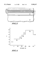
- FIG. 1 includes an illustration of a cross-sectional view of a portion of a semiconductor substrate after forming an antireflective layer in accordance with one embodiment of the present invention
- FIG. 2 includes a plot of refractive index as a function of distance from an interface between oxide and antireflective layers
- FIG. 3 includes an illustration of a cross-sectional view of a portion of a semiconductor substrate after forming an antireflective layer in accordance with another embodiment of the present invention
- FIG. 4 includes a plot of refractive index as a function of distance from an interface between oxide and antireflective layers
- FIG. 5 includes an illustration of a cross-sectional view of a portion of a semiconductor substrate after forming an antireflective layer in accordance with yet another embodiment of the present invention
- FIG. 6 includes a plot of refractive index as a function of distance from an interface between oxide and antireflective layers
- FIG. 7 includes an illustration of a cross-sectional view of a portion of a semiconductor substrate after forming a photoresist members
- FIG. 8 includes an illustration of a cross-sectional view of the substrate of FIG. 7 after forming gate electrode structures
- FIG. 9 includes an illustration of a cross-sectional view of the substrate of FIG. 6 after forming spacers and doped regions;
- FIG. 10 includes an illustration of a cross-sectional view of the substrate of FIG. 9 after forming another photoresist members
- FIG. 11 includes a cross-sectional view of the substrate of FIG. 10 after forming a contact structure
- FIG. 12 includes an illustration of a cross-sectional view of the substrate of FIG. 9 after forming an interconnecting layer and still another antireflective layer;
- FIG. 13 includes an illustration of the substrate of FIG. 12 after forming a substantially completed device.
- the embodiments described below include a nitrogen-containing antireflective layer that either has a continuously graded composition or includes a plurality of discrete portions that make up the antireflective layer.
- the antireflective layer allows a low reflectance antireflective layer to be formed that can be integrated into an existing process without causing other problems. Compare this with the prior art that has a single layer of relatively uniform composition that could have adherence, current leakage, or reactivity problems.
- the present invention is better understood with the embodiments described below.
- the embodiments described below have an antireflective layer that is typically inorganic.
- One location of the antireflective layer that is closer to a substrate typically has a formula of M a N b O c , and another location further from the substrate has a formula of X d N e O f .
- M and X are any element, although they usually are silicon, germanium, boron, phosphorus, aluminum, molybdenum, tantalum, titanium, tungsten, or the like. M and X can be the same element or different elements.
- N is nitrogen
- O oxygen. The two locations have different compositions even if M and X are the same element.
- a, b, d, and e are greater than zero because nitride-containing materials make good antireflective layers. If one of the portions is silicon-rich silicon nitride, M is silicon, a/b is greater than 3/4, and c is 0. For silicon oxynitride, M is silicon, and a, b, and c are greater than zero.
- Stoichiometric silicon nitride is Si 3 N 4 . As used in this specification, stoichiometric means that the composition is such that the ratio of the elements is capable of forming a neutrally charged, entirely molecular compound. Silicon-rich silicon nitride and silicon oxynitride are examples of nonstoichiometric materials.
- the antireflective layer is typically formed by low pressure chemical vapor deposition at a temperature of at least 600 degrees Celsius, plasma-enhanced chemical vapor deposition at a temperature no higher than 480 degrees Celsius, or sputter deposition using multiple targets or reactive sputtering.
- the antireflective layer typically has a thickness in a range of 100-1000 angstroms and often has a thickness in a range of 200-500 angstroms.
- M and X are typically metals, and the subscripts for c and f are typically zero.
- metals include aluminum, molybdenum, tantalum, titanium, and tungsten, or the like.
- Many metal oxides are insulators and the use of such materials can cause high via resistance or difficulties at wiring bonding.
- one embodiment can be as simple as using a portion that includes silicon-rich silicon nitride and a portion that includes stoichiometric silicon nitride. Note that the two portions are at different locations with the antireflective layer and have the same elements (silicon and nitrogen) but different compositions.
- Stoichiometric silicon nitride is an insulator and prevents conductive members from being electrically connected to each other.
- the silicon-rich silicon nitride portion allows the antireflective layer to have a lower reflectance than stoichiometric silicon nitride by itself.
- the antireflective layer can include a layer having continuous change in refractive index or discrete portions or layers having relatively smaller changes in refractive indices.
- semiconductor substrate 10 is covered by dielectric layer 12, polysilicon layer 14, titanium silicide layer 16, antireflective layer 18, and oxide layer 20.
- FIG. 2 includes a plot of refractive index as a function of distance from the interface between oxide layer 20 and antireflective layer 18.
- FIG. 3 includes another embodiment using a plurality of discrete portions. Referring to FIG. 3, antireflective layer 18 is replaced by antireflective layer 28 that includes portions 280, 282, 284, 286, and 288.
- Portions 280, 282, 284, 286 are silicon-rich silicon nitride layers that have decreasing amounts of silicon (i.e., portion 280 has a higher silicon to nitrogen ratio compared to portion 282, etc.). These layers include the same elements but have different compositions. Portion 288 includes silicon oxynitride.
- FIG. 4 includes a plot of refractive index as a function of distance from the oxide layer 20 towards the titanium silicide layer 16.
- antireflective layer 38 includes portions 380, 382, and 384 that are at different locations in the antireflective layer 38.
- Portion 382 has a higher absorption coefficient than portions 380 and 384.
- portion 382 has a higher refractive index than each of the oxide layers 20 and 36 and each of the portions 380 and 384.
- portion 382 might need to be protected because it is too conductive, water soluble, etches in chemistry similar to an overlying layer (i.e., oxide layer 20), has an undesired reaction with an immediately adjacent layer, does not adhere well to oxide, or some other reason.
- FIG. 6 includes a plot of refractive index as a function of a distance from the interface between the oxide and antireflective layers 20 and 38, respectively.
- Portion 380 is a protective layer for portion 382.
- Portion 380 is typically only as thick as needed to act as a protective layer and is typically no more than 75 angstroms thick.
- portions 380, 382, and 384 are 50, 100, and 200 angstroms thick, respectively.
- All the refractive indices given within this example are at a wavelength of 365 nanometers that generally corresponds to the i-line of visible radiation. Absorption and refractive index for a material typically change with a change in the radiation source. For example, an antireflective layer that is optimal for a wavelength of 365 nanometers may need changed to be optimal for 248 nanometers (deep ultraviolet).
- the present invention is not limited to the visible light spectrum. Radiation outside of the visible light spectrum may be used, although composition and thickness of the antireflective layer may need to be optimized for the radiation used.
- FIG. 7 includes a cross-sectional view of a portion of a semiconductor substrate 50, such as p-type monocrystalline silicon.
- Field isolation regions 51 and a gate dielectric layer 52 overlie the substrate 50.
- a doped polysilicon layer 53 is formed over the gate dielectric layer and the field isolation regions.
- An antireflective layer 54 is formed over the doped polysilicon layer 53.
- the antireflective layer 54 includes a silicon-rich silicon nitride portion 541 and a stoichiometric silicon nitride portion 542.
- a photoresist layer is coated over the substrate and is patterned to form photoresist members 55 and openings 56 as shown in FIG. 7. The patterning of the photoresist members 55 is less likely to result in reflective notching or other complications because of the presence of the antireflective layer 54 that includes portions 541 and 542.
- the layers 52-54 are patterned to form gate structures 60 as shown in FIG. 8.
- the antireflective layer 54 is etched using a fluorine-containing gas that includes carbon tetrafluoride, trifluoromethane, or the like. In one specific embodiment, the antireflective layer 54 is etched using a combination of carbon tetrafluoride and trifluoromethane.
- the layers 52 and 53 are etched using conventional etching techniques.
- the photoresist members 55 are removed using a plasma ashing process. Alternatively, both the photoresist members and the antireflective layer could be removed, thereby leaving the patterned portions of layers 52 and 53 as gate structures 60.
- the substrate is further processed to form sidewall spacers 74 and doped regions 72 within the substrate 50 adjacent to the gate structures 60 as shown in FIG. 9.
- the spacers 74 include oxide, nitride, or a combination of these materials.
- Doped regions 72 are source/drain regions near the gate structures 60.
- An insulating layer 80 is formed over the substrate and patterned to form an opening over the center doped region 72 as shown in FIG. 10.
- a doped polysilicon layer 82, a tungsten silicide layer 84, and an antireflective layer 86 are formed over the substrate 50 and insulating layer 80.
- the antireflective layer 86 includes tungsten-rich tungsten nitride portions 861 and 862 and a stoichiometric tungsten nitride portion 863. Note that the portions 861-863 have increasing amounts of nitrogen as the distance from the substrate 50 increases. When comparing portions 861 and 862, portion 861 is the more tungsten rich.
- a photoresist layer is formed and patterned over the antireflective layer 86 to form a photoresist member 88.
- the antireflective layer 86, the tungsten silicide layer 84, and doped polysilicon layer 82 are then patterned to form a contact structure 90 as shown in FIG. 11.
- the photoresist member 88 is removed. As can be seen in FIG. 11, the contact structure 90 makes contact to the center doped region 72.
- Other contact structures similar to contact structure 90 are formed but are not shown in FIG. 11.
- the antireflective layer 86 could be removed if this is so desired. Alternatively, only a portion of it could be removed.
- the antireflective layer 54 was a single layer of silicon-rich silicon nitride, an electrical leakage path would be formed between the contact structure 90 and the doped polysilicon layer 53. In essence, a source/drain region (center doped region 72) is resistively connected to the gate electrodes (polysilicon layer 53) of the gate structures.
- a leakage path is not formed between the center doped region 72 and the polysilicon layer 53 of the gate structures as shown in FIG. 11. Clearly, a leakage path is undesired.
- An insulating layer 100 is formed over the contact structure 90 and the rest of the substrate 50 and is patterned to form contact openings 102 as shown in FIG. 12.
- the contact openings 102 are filled with a conductive material to form contact plugs 104.
- the contact plugs 104 include tungsten and adhesion or barrier layers.
- a barrier layer 106, an interconnecting layer 108, and an antireflective layer 109 are formed.
- an adhesion layer lies between the oxide and barrier layers 100 and 106 but is not shown in FIG. 12.
- the choice of materials for layers 106 and 109 depends upon the selection of materials for interconnecting layer 108.
- the interconnecting layer 108 includes aluminum
- the barrier layer 106 could include titanium nitride
- the antireflective layer 109 could include an aluminum-rich aluminum nitride portion 1091 and a stoichiometric aluminum nitride portion 1092.
- the interconnecting layer 108 includes copper
- the barrier layer 106 could include tantalum, molybdenum, tantalum-containing or molybdenum-containing materials, or the like, and the antireflective layer 109 includes a lower portion 1091 and an upper portion 1092.
- the lower portion 1091 typically includes tantalum-rich tantalum nitride or molybdenum-rich molybdenum nitride
- the upper portion 1092 typically includes stoichiometric tantalum nitride or stoichiometric molybdenum nitride.
- Layers 106, 108, and 109 are patterned to form interconnects 112 and 114 as shown in FIG. 13.
- the interconnects 112 and 114 and insulating layer 100 are covered by a passivation layer 116.
- the materials used for the passivation layer depend upon the materials of the interconnecting layer 108. For example, if the interconnecting layer 108 includes aluminum, the passivation layer includes oxide, nitride, or oxynitride. However, if the interconnecting layer 108 includes copper, the passivation layer 116 includes a nitride layer immediately adjacent to the copper to prevent any out diffusion that would possibly occur if oxide would contact the copper.
- the interconnects 112 and 114 are electrically connected to the outer doped regions 72 within substrate 50. Other electrical connections are made within the semiconductor device shown in FIG. 13 but are not shown. For example, electrical connections are made to the contact structure 90 and the polysilicon layer 53 but are not shown in FIG. 13. If needed, other insulating layers and interconnecting levels could be formed.
- any of the antireflective layer could a single layer having a continuously graded composition rather than discreet portions.
- antireflective layer 54 could be formed such that the silicon to nitrogen ratio decreases as the layer becomes thicker.
- the continuously graded antireflective layer would be formed by decreasing the silicon source gas flow rate or increasing the nitrogen source gas flow rate while varying other deposition parameter(s), such as power, pressure, spacing, etc., so as to maintain the desired film properties (i.e., uniformity, etch rate, etc.) during the deposition.
- this single layer includes a location near the polysilicon layer 53 that has a different composition than another location of that single layer further from the polysilicon layer 53.
- portions 861 and 862 have tungsten and nitrogen, and portion 863 includes stoichiometric silicon nitride. In this manner, portion 863 is an insulator. In alternate embodiments, other materials are used for other reasons that are not related to lithographic issues. In still other embodiments, an antireflective layer could include a nitrogen rich portion.
- an antireflective layer is nonstoichiometric. In some embodiments, all portions may be nonstoichiometric.
- portion 542 stoichiometric silicon nitride can be replaced by nitrogen-rich silicon nitride. In this manner, antireflective layer 54 only has nonstoichiometric portions.
- a uniform composition antireflective layer as used in the prior art can be too reflective, form a leakage path, can be water soluble, etch in chemistry used to etch an overlying layer, can have an undesired reaction with an immediately adjacent layer, may not adhere well to underlying or overlying layers, or cause some other problem.
- An antireflective layer formed in accordance with the present invention can be formed to give low reflectance without any of the problems listed above.
- the antireflective layer can be integrated into an existing process flow without having to use marginal processing steps.
Abstract
Description
Claims (42)
Priority Applications (4)
| Application Number | Priority Date | Filing Date | Title |
|---|---|---|---|
| US08/413,021 US5918147A (en) | 1995-03-29 | 1995-03-29 | Process for forming a semiconductor device with an antireflective layer |
| TW085101797A TW350989B (en) | 1995-03-29 | 1996-02-13 | Process for forming a semiconductor device with an antireflective layer |
| JP8093676A JPH08274023A (en) | 1995-03-29 | 1996-03-22 | Method of manufacturing semiconductor device with reflectionreducing layer |
| KR1019960009001A KR960035773A (en) | 1995-03-29 | 1996-03-29 | Method for forming a semiconductor device having an antireflection layer |
Applications Claiming Priority (1)
| Application Number | Priority Date | Filing Date | Title |
|---|---|---|---|
| US08/413,021 US5918147A (en) | 1995-03-29 | 1995-03-29 | Process for forming a semiconductor device with an antireflective layer |
Publications (1)
| Publication Number | Publication Date |
|---|---|
| US5918147A true US5918147A (en) | 1999-06-29 |
Family
ID=23635466
Family Applications (1)
| Application Number | Title | Priority Date | Filing Date |
|---|---|---|---|
| US08/413,021 Expired - Fee Related US5918147A (en) | 1995-03-29 | 1995-03-29 | Process for forming a semiconductor device with an antireflective layer |
Country Status (4)
| Country | Link |
|---|---|
| US (1) | US5918147A (en) |
| JP (1) | JPH08274023A (en) |
| KR (1) | KR960035773A (en) |
| TW (1) | TW350989B (en) |
Cited By (45)
| Publication number | Priority date | Publication date | Assignee | Title |
|---|---|---|---|---|
| US6004850A (en) * | 1998-02-23 | 1999-12-21 | Motorola Inc. | Tantalum oxide anti-reflective coating (ARC) integrated with a metallic transistor gate electrode and method of formation |
| US6078091A (en) * | 1998-04-22 | 2000-06-20 | Clear Logic, Inc. | Inter-conductive layer fuse for integrated circuits |
| US6100559A (en) * | 1998-08-14 | 2000-08-08 | Advanced Micro Devices, Inc. | Multipurpose graded silicon oxynitride cap layer |
| US6153504A (en) * | 1999-08-16 | 2000-11-28 | Advanced Micro Devices, Inc. | Method of using a silicon oxynitride ARC for final metal layer |
| US6221712B1 (en) * | 1999-08-30 | 2001-04-24 | United Microelectronics Corp. | Method for fabricating gate oxide layer |
| US6294460B1 (en) * | 2000-05-31 | 2001-09-25 | Advanced Micro Devices, Inc. | Semiconductor manufacturing method using a high extinction coefficient dielectric photomask |
| US6297171B1 (en) | 1995-12-04 | 2001-10-02 | Micron Technology Inc. | Semiconductor processing method of promoting photoresist adhesion to an outer substrate layer predominately comprising silicon nitride |
| US6300253B1 (en) * | 1998-04-07 | 2001-10-09 | Micron Technology, Inc. | Semiconductor processing methods of forming photoresist over silicon nitride materials, and semiconductor wafer assemblies comprising photoresist over silicon nitride materials |
| US6316372B1 (en) | 1998-04-07 | 2001-11-13 | Micron Technology, Inc. | Methods of forming a layer of silicon nitride in a semiconductor fabrication process |
| US6323139B1 (en) * | 1995-12-04 | 2001-11-27 | Micron Technology, Inc. | Semiconductor processing methods of forming photoresist over silicon nitride materials |
| US6326231B1 (en) * | 1998-12-08 | 2001-12-04 | Advanced Micro Devices, Inc. | Use of silicon oxynitride ARC for metal layers |
| US6355546B1 (en) * | 1999-08-11 | 2002-03-12 | Advanced Micro Devices, Inc. | Thermally grown protective oxide buffer layer for ARC removal |
| US6410443B1 (en) * | 1999-08-27 | 2002-06-25 | Advanced Micro Devices, Inc. | Method for removing semiconductor ARC using ARC CMP buffing |
| US20020097493A1 (en) * | 2000-04-27 | 2002-07-25 | Guoguang Li | Graded anti-reflective coatings for photolithography |
| US6429151B1 (en) | 1998-04-07 | 2002-08-06 | Micron Technology, Inc. | Semiconductor wafer assemblies comprising silicon nitride, methods of forming silicon nitride, and methods of reducing stress on semiconductive wafers |
| US6436805B1 (en) | 1999-09-01 | 2002-08-20 | Micron Technology, Inc. | Local interconnect structures and methods for making the same |
| US6492701B1 (en) * | 1998-06-29 | 2002-12-10 | Samsung Electronics Co. Ltd. | Semiconductor device having anti-reflective cap and spacer, method of manufacturing the same, and method of manufacturing photoresist pattern using the same |
| WO2002099857A1 (en) * | 2001-06-06 | 2002-12-12 | Advanced Micro Devices, Inc. | Anti-reflective coating and methods of making the same |
| DE10163312A1 (en) * | 2001-12-21 | 2003-02-27 | Infineon Technologies Ag | Semiconductor structure manufacture, conducting layer formed on semiconductor substrate has covering layer that has continuous stoichiometric gradient from a metal to a metal/non-metal compound |
| US6534398B2 (en) | 1998-06-17 | 2003-03-18 | Cypress Semiconductor Corp. | Method of forming metal layer(s) and/or antireflective coating layer(s) on an integrated circuit |
| US6576967B1 (en) | 2000-09-18 | 2003-06-10 | Motorola, Inc. | Semiconductor structure and process for forming a metal oxy-nitride dielectric layer |
| US6635530B2 (en) | 1998-04-07 | 2003-10-21 | Micron Technology, Inc. | Methods of forming gated semiconductor assemblies |
| US6686633B1 (en) | 1997-12-23 | 2004-02-03 | Motorola, Inc. | Semiconductor device, memory cell, and processes for forming them |
| US6689682B1 (en) * | 2000-08-11 | 2004-02-10 | Advanced Micro Devices, Inc. | Multilayer anti-reflective coating for semiconductor lithography |
| US20040145029A1 (en) * | 2003-01-29 | 2004-07-29 | Adetutu Olubunmi O. | A method of forming an arc layer for a semiconductor device |
| US20040219709A1 (en) * | 2003-04-29 | 2004-11-04 | Won-Ho Lee | Method for fabricating complementary metal oxide semiconductor image sensor |
| US20040222525A1 (en) * | 1997-03-14 | 2004-11-11 | Rhodes Howard E. | Advanced VLSI metallization |
| US20040225300A1 (en) * | 1999-04-09 | 2004-11-11 | Evalve, Inc. | Methods and devices for capturing and fixing leaflets in valve repair |
| US20050003671A1 (en) * | 1997-04-02 | 2005-01-06 | United Microelectronics Corporation | High density plasma chemical vapor deposition process |
| US20050032545A1 (en) * | 2000-07-14 | 2005-02-10 | Chang Donald C. D. | Fixed wireless back haul for mobile communications using stratospheric platforms |
| US20050087870A1 (en) * | 2003-10-23 | 2005-04-28 | Adetutu Olubunmi O. | Semiconductor device and method of forming the same |
| US6903007B1 (en) * | 1995-06-07 | 2005-06-07 | Advanced Micro Devices, Inc. | Process for forming bottom anti-reflection coating for semiconductor fabrication photolithography which inhibits photoresist footing |
| US7060584B1 (en) * | 1999-07-12 | 2006-06-13 | Zilog, Inc. | Process to improve high performance capacitor properties in integrated MOS technology |
| US20060197096A1 (en) * | 2003-10-30 | 2006-09-07 | Sebastien Kerdiles | Substrate with refractive index matching |
| US20070037078A1 (en) * | 2005-08-11 | 2007-02-15 | Samsung Electronics Co., Ltd. | Reference wafer for calibrating semiconductor equipment |
| US20080196626A1 (en) * | 2007-02-20 | 2008-08-21 | Hengpeng Wu | Silicone coating composition |
| EP1983559A1 (en) * | 2006-02-07 | 2008-10-22 | Fujitsu Ltd. | Semiconductor device and process for producing the same |
| US20090159321A1 (en) * | 2007-12-21 | 2009-06-25 | Spansion Llc | Electronic devices with ultraviolet blocking layers and processes of forming the same |
| WO2009133456A1 (en) * | 2008-04-30 | 2009-11-05 | Az Electronic Materials Usa Corp. | Spin-on graded k silicon antireflective coating |
| US20100093969A1 (en) * | 2007-02-26 | 2010-04-15 | Ruzhi Zhang | Process for making siloxane polymers |
| US20100291475A1 (en) * | 2009-05-12 | 2010-11-18 | Chenghong Li | Silicone Coating Compositions |
| US20110284068A1 (en) * | 2010-04-23 | 2011-11-24 | Solexel, Inc. | Passivation methods and apparatus for achieving ultra-low surface recombination velocities for high-efficiency solar cells |
| US8524441B2 (en) | 2007-02-27 | 2013-09-03 | Az Electronic Materials Usa Corp. | Silicon-based antireflective coating compositions |
| US10368729B2 (en) | 2005-02-02 | 2019-08-06 | Intuitive Surgical Operations, Inc. | Methods and apparatus for efficient purging |
| US20210217625A1 (en) * | 2020-01-09 | 2021-07-15 | Samsung Electronics Co., Ltd. | Methods of cutting a fine pattern, methods of forming active patterns using the same, and methods of manufacturing a semiconductor device using the same |
Citations (25)
| Publication number | Priority date | Publication date | Assignee | Title |
|---|---|---|---|---|
| US4488775A (en) * | 1981-05-26 | 1984-12-18 | Olympus Optical Co., Ltd. | Light absorptive film having an anti-reflecting property |
| US4545646A (en) * | 1983-09-02 | 1985-10-08 | Hughes Aircraft Company | Process for forming a graded index optical material and structures formed thereby |
| JPS6441852A (en) * | 1987-08-10 | 1989-02-14 | Taiyo Yuden Kk | Hydrogen ion sensitive semiconductor sensor |
| JPS6447082A (en) * | 1987-08-18 | 1989-02-21 | Fujitsu Ltd | Semiconductor light-emitting element |
| US4820611A (en) * | 1987-04-24 | 1989-04-11 | Advanced Micro Devices, Inc. | Titanium nitride as an antireflection coating on highly reflective layers for photolithography |
| JPH01241125A (en) * | 1988-03-23 | 1989-09-26 | Sony Corp | Manufacture of semiconductor device |
| WO1989009494A1 (en) * | 1988-03-31 | 1989-10-05 | Solarex Corporation | Gate dielectric for a thin film field effect transistor |
| US4968117A (en) * | 1983-09-02 | 1990-11-06 | Hughes Aircraft Company | Graded index asperhic combiners and display system utilizing same |
| US4990995A (en) * | 1987-09-08 | 1991-02-05 | General Electric Company | Low reflectance conductor in an integrated circuit |
| US5037777A (en) * | 1990-07-02 | 1991-08-06 | Motorola Inc. | Method for forming a multi-layer semiconductor device using selective planarization |
| US5066615A (en) * | 1989-10-23 | 1991-11-19 | At&T Bell Laboratories | Photolithographic processes using thin coatings of refractory metal silicon nitrides as antireflection layers |
| GB2246905A (en) * | 1990-08-09 | 1992-02-12 | British Telecomm | Multi-layered antireflective coatings for optoelectronic components |
| US5091244A (en) * | 1990-08-10 | 1992-02-25 | Viratec Thin Films, Inc. | Electrically-conductive, light-attenuating antireflection coating |
| US5135877A (en) * | 1990-10-09 | 1992-08-04 | Eastman Kodak Company | Method of making a light-emitting diode with anti-reflection layer optimization |
| US5219793A (en) * | 1991-06-03 | 1993-06-15 | Motorola Inc. | Method for forming pitch independent contacts and a semiconductor device having the same |
| DE4311761A1 (en) * | 1992-04-16 | 1993-10-21 | Mitsubishi Electric Corp | Silicon nitride anti-reflection film prodn. for use in photolithographic steps of semiconductor device mfr. - by selecting optical characteristic of film, by determining values of real and imaginary parts of specified relationship |
| US5258643A (en) * | 1991-07-25 | 1993-11-02 | Massachusetts Institute Of Technology | Electrically programmable link structures and methods of making same |
| US5292417A (en) * | 1991-04-12 | 1994-03-08 | Balzers Aktiengesellschaft | Method for reactive sputter coating at least one article |
| EP0588087A2 (en) * | 1992-08-20 | 1994-03-23 | Sony Corporation | Method of determining optimum optical conditions for an anti-reflective layer used in a method of forming a resist pattern |
| US5378659A (en) * | 1993-07-06 | 1995-01-03 | Motorola Inc. | Method and structure for forming an integrated circuit pattern on a semiconductor substrate |
| US5428244A (en) * | 1992-06-29 | 1995-06-27 | Matsushita Electric Industrial Co., Ltd. | Semiconductor device having a silicon rich dielectric layer |
| US5488246A (en) * | 1993-04-16 | 1996-01-30 | Mitsubishi Denki Kabushiki Kaisha | Semiconductor device and method of manufacturing the same |
| US5525542A (en) * | 1995-02-24 | 1996-06-11 | Motorola, Inc. | Method for making a semiconductor device having anti-reflective coating |
| US5595938A (en) * | 1993-12-28 | 1997-01-21 | Mitsubishi Denki Kabushiki Kaisha | Method of manufacturing semiconductor device |
| US5643806A (en) * | 1993-02-28 | 1997-07-01 | Sony Corporation | Manufacturing method for making bipolar device |
-
1995
- 1995-03-29 US US08/413,021 patent/US5918147A/en not_active Expired - Fee Related
-
1996
- 1996-02-13 TW TW085101797A patent/TW350989B/en not_active IP Right Cessation
- 1996-03-22 JP JP8093676A patent/JPH08274023A/en active Pending
- 1996-03-29 KR KR1019960009001A patent/KR960035773A/en not_active Application Discontinuation
Patent Citations (26)
| Publication number | Priority date | Publication date | Assignee | Title |
|---|---|---|---|---|
| US4488775A (en) * | 1981-05-26 | 1984-12-18 | Olympus Optical Co., Ltd. | Light absorptive film having an anti-reflecting property |
| US4545646A (en) * | 1983-09-02 | 1985-10-08 | Hughes Aircraft Company | Process for forming a graded index optical material and structures formed thereby |
| US4968117A (en) * | 1983-09-02 | 1990-11-06 | Hughes Aircraft Company | Graded index asperhic combiners and display system utilizing same |
| US4820611A (en) * | 1987-04-24 | 1989-04-11 | Advanced Micro Devices, Inc. | Titanium nitride as an antireflection coating on highly reflective layers for photolithography |
| JPS6441852A (en) * | 1987-08-10 | 1989-02-14 | Taiyo Yuden Kk | Hydrogen ion sensitive semiconductor sensor |
| JPS6447082A (en) * | 1987-08-18 | 1989-02-21 | Fujitsu Ltd | Semiconductor light-emitting element |
| US4990995A (en) * | 1987-09-08 | 1991-02-05 | General Electric Company | Low reflectance conductor in an integrated circuit |
| JPH01241125A (en) * | 1988-03-23 | 1989-09-26 | Sony Corp | Manufacture of semiconductor device |
| WO1989009494A1 (en) * | 1988-03-31 | 1989-10-05 | Solarex Corporation | Gate dielectric for a thin film field effect transistor |
| US5066615A (en) * | 1989-10-23 | 1991-11-19 | At&T Bell Laboratories | Photolithographic processes using thin coatings of refractory metal silicon nitrides as antireflection layers |
| US5037777A (en) * | 1990-07-02 | 1991-08-06 | Motorola Inc. | Method for forming a multi-layer semiconductor device using selective planarization |
| GB2246905A (en) * | 1990-08-09 | 1992-02-12 | British Telecomm | Multi-layered antireflective coatings for optoelectronic components |
| US5091244A (en) * | 1990-08-10 | 1992-02-25 | Viratec Thin Films, Inc. | Electrically-conductive, light-attenuating antireflection coating |
| US5135877A (en) * | 1990-10-09 | 1992-08-04 | Eastman Kodak Company | Method of making a light-emitting diode with anti-reflection layer optimization |
| US5292417A (en) * | 1991-04-12 | 1994-03-08 | Balzers Aktiengesellschaft | Method for reactive sputter coating at least one article |
| US5219793A (en) * | 1991-06-03 | 1993-06-15 | Motorola Inc. | Method for forming pitch independent contacts and a semiconductor device having the same |
| US5258643A (en) * | 1991-07-25 | 1993-11-02 | Massachusetts Institute Of Technology | Electrically programmable link structures and methods of making same |
| DE4311761A1 (en) * | 1992-04-16 | 1993-10-21 | Mitsubishi Electric Corp | Silicon nitride anti-reflection film prodn. for use in photolithographic steps of semiconductor device mfr. - by selecting optical characteristic of film, by determining values of real and imaginary parts of specified relationship |
| US5428244A (en) * | 1992-06-29 | 1995-06-27 | Matsushita Electric Industrial Co., Ltd. | Semiconductor device having a silicon rich dielectric layer |
| EP0588087A2 (en) * | 1992-08-20 | 1994-03-23 | Sony Corporation | Method of determining optimum optical conditions for an anti-reflective layer used in a method of forming a resist pattern |
| US5643806A (en) * | 1993-02-28 | 1997-07-01 | Sony Corporation | Manufacturing method for making bipolar device |
| US5488246A (en) * | 1993-04-16 | 1996-01-30 | Mitsubishi Denki Kabushiki Kaisha | Semiconductor device and method of manufacturing the same |
| US5378659A (en) * | 1993-07-06 | 1995-01-03 | Motorola Inc. | Method and structure for forming an integrated circuit pattern on a semiconductor substrate |
| US5539249A (en) * | 1993-07-06 | 1996-07-23 | Motorola, Inc. | Method and structure for forming an integrated circuit pattern on a semiconductor substrate |
| US5595938A (en) * | 1993-12-28 | 1997-01-21 | Mitsubishi Denki Kabushiki Kaisha | Method of manufacturing semiconductor device |
| US5525542A (en) * | 1995-02-24 | 1996-06-11 | Motorola, Inc. | Method for making a semiconductor device having anti-reflective coating |
Non-Patent Citations (28)
| Title |
|---|
| Czech, et al., "Reduction of Linewidth Variation for the Gate Conductor Level by Lithography Based on a New Antireflective Layer," Microelectronic Engineering 21; pp. 51-60 (1993). |
| Czech, et al., Reduction of Linewidth Variation for the Gate Conductor Level by Lithography Based on a New Antireflective Layer, Microelectronic Engineering 21; pp. 51 60 (1993). * |
| Dijkstra, et al, "Optimization of Anti-Reflection Layers for Deep UV Lithography," SPIE vol. 1927, Optical/Laser Microlithography VI; pp. 275-286 (1993). |
| Dijkstra, et al, Optimization of Anti Reflection Layers for Deep UV Lithography, SPIE vol. 1927, Optical/Laser Microlithography VI; pp. 275 286 (1993). * |
| Gordon, et al., "Chemical Vapor Deposition of Aluminum Nitride Thin Films," J. Mater. Res. vol. 7, No. 7; pp. 1679-1684 (1992). |
| Gordon, et al., Chemical Vapor Deposition of Aluminum Nitride Thin Films, J. Mater. Res. vol. 7, No. 7; pp. 1679 1684 (1992). * |
| Johnson, et al., "Plasma-Enhanced CVD Silicon Nitride Antireflection Coatings for Solar Cells," Solar Energy; pp. 355-358 (1983). |
| Johnson, et al., Plasma Enhanced CVD Silicon Nitride Antireflection Coatings for Solar Cells, Solar Energy; pp. 355 358 (1983). * |
| Kanicki, "Roll of Hydrogen in Silicon Nitride Films Prepared by Various Deposition Techniques," Mat. Res. Soc. Symp. Proc., vol. 118, pp. 671-677 (1988). |
| Kanicki, Roll of Hydrogen in Silicon Nitride Films Prepared by Various Deposition Techniques, Mat. Res. Soc. Symp. Proc., vol. 118, pp. 671 677 (1988). * |
| Kim, et al., "Amorphous Silicon Thin-Film Transistors with Two-Layer Gate Insulator," Appl. Phys. Lett. 54, No. 21; pp. 2079-2081 (1989). |
| Kim, et al., Amorphous Silicon Thin Film Transistors with Two Layer Gate Insulator, Appl. Phys. Lett. 54, No. 21; pp. 2079 2081 (1989). * |
| Kumar, et al., "Growth and Properties of TiN and TiOxNy Diffusion Barriers in Silicon on Sapphire Integrated Circuits," Thin Solid Films, 153: pp. 287-301 (1987). |
| Kumar, et al., Growth and Properties of TiN and TiOxNy Diffusion Barriers in Silicon on Sapphire Integrated Circuits, Thin Solid Films, 153: pp. 287 301 (1987). * |
| Lau, et al., "Stability of Electrical Properties of Nitrogen-Rich, Silicon-Rich, and Stoichiometric Silicon Nitride Films," J. Appl. Phys., vol. 66, No. 6; pp. 2765-2767 (1989). |
| Lau, et al., Stability of Electrical Properties of Nitrogen Rich, Silicon Rich, and Stoichiometric Silicon Nitride Films, J. Appl. Phys., vol. 66, No. 6; pp. 2765 2767 (1989). * |
| Legrand, et al., "Optical Properties of Sputter-Deposited Aluminum Nitride Films on Silicon," Thin Solid Films, 248; pp. 220-223 (1994). |
| Legrand, et al., Optical Properties of Sputter Deposited Aluminum Nitride Films on Silicon, Thin Solid Films, 248; pp. 220 223 (1994). * |
| Pampalone, et al., "Improved Photoresist Patterning over Reflective Topographies Using Titanium Oxynitride Antireflection Coatings," J. Electrochem. Soc., vol. 136, No. 4; pp. 1181-1185 (1989). |
| Pampalone, et al., Improved Photoresist Patterning over Reflective Topographies Using Titanium Oxynitride Antireflection Coatings, J. Electrochem. Soc., vol. 136, No. 4; pp. 1181 1185 (1989). * |
| Polasko, et al., "Thin Silicon Films used as Antireflection Coatings for Metal Coated Substrates," SPIE vol. 631, Advances in Resist Technology and Processing III; pp. 180-186 (1986). |
| Polasko, et al., Thin Silicon Films used as Antireflection Coatings for Metal Coated Substrates, SPIE vol. 631, Advances in Resist Technology and Processing III; pp. 180 186 (1986). * |
| Schattenburg, et al., "Fabrication and Testing of 0.1-um-Linewidth Microgap X-Ray Masks," J. Vac. Sci. Technol. B 8 (6); pp. 1604-1608 (1990). |
| Schattenburg, et al., Fabrication and Testing of 0.1 um Linewidth Microgap X Ray Masks, J. Vac. Sci. Technol. B 8 (6); pp. 1604 1608 (1990). * |
| Wittmer, "Properties and Microelectronic Applications of Thin Films of Refractory Metal Nitrides," J. Vac. Sci. Technol. A 3 (4); pp. 1797-1803 (1985). |
| Wittmer, Properties and Microelectronic Applications of Thin Films of Refractory Metal Nitrides, J. Vac. Sci. Technol. A 3 (4); pp. 1797 1803 (1985). * |
| Yu, et al., "Deposition, Characterization, and Application of Aluminum Nitride Thin Films for Microelectronics," Mat. Res. Soc. Symp. Proc. vol. 264; pp. 401-405 (1992). |
| Yu, et al., Deposition, Characterization, and Application of Aluminum Nitride Thin Films for Microelectronics, Mat. Res. Soc. Symp. Proc. vol. 264; pp. 401 405 (1992). * |
Cited By (88)
| Publication number | Priority date | Publication date | Assignee | Title |
|---|---|---|---|---|
| US6903007B1 (en) * | 1995-06-07 | 2005-06-07 | Advanced Micro Devices, Inc. | Process for forming bottom anti-reflection coating for semiconductor fabrication photolithography which inhibits photoresist footing |
| US6323139B1 (en) * | 1995-12-04 | 2001-11-27 | Micron Technology, Inc. | Semiconductor processing methods of forming photoresist over silicon nitride materials |
| US7057263B2 (en) | 1995-12-04 | 2006-06-06 | Micron Technology, Inc. | Semiconductor wafer assemblies comprising photoresist over silicon nitride materials |
| US6297171B1 (en) | 1995-12-04 | 2001-10-02 | Micron Technology Inc. | Semiconductor processing method of promoting photoresist adhesion to an outer substrate layer predominately comprising silicon nitride |
| US20040124441A1 (en) * | 1995-12-04 | 2004-07-01 | Moore John T. | Semiconductor wafer assemblies comprising photoresist over silicon nitride materials |
| US6693345B2 (en) | 1995-12-04 | 2004-02-17 | Micron Technology, Inc. | Semiconductor wafer assemblies comprising photoresist over silicon nitride materials |
| US6451504B2 (en) | 1995-12-04 | 2002-09-17 | Micron Technology, Inc. | Semiconductor processing method of promoting photoresist adhesion to an outer substrate layer predominately comprising silicon nitride |
| US6417559B1 (en) | 1995-12-04 | 2002-07-09 | Micron Technology, Inc. | Semiconductor wafer assemblies comprising photoresist over silicon nitride materials |
| US7943505B2 (en) | 1997-03-14 | 2011-05-17 | Micron Technology, Inc. | Advanced VLSI metallization |
| US20040229455A1 (en) * | 1997-03-14 | 2004-11-18 | Rhodes Howard E. | Advanced VLSI metallization |
| US20040222525A1 (en) * | 1997-03-14 | 2004-11-11 | Rhodes Howard E. | Advanced VLSI metallization |
| US20100173490A1 (en) * | 1997-04-02 | 2010-07-08 | Chih-Chien Liu | High density plasma chemical vapor deposition process |
| US7514014B1 (en) | 1997-04-02 | 2009-04-07 | United Microelectronics Corporation | High density plasma chemical vapor deposition process |
| US7078346B2 (en) | 1997-04-02 | 2006-07-18 | United Microelectronics Corporation | High density plasma chemical vapor deposition process |
| US20060099824A1 (en) * | 1997-04-02 | 2006-05-11 | Chih-Chien Liu | High density plasma chemical vapor deposition process |
| US7718079B2 (en) | 1997-04-02 | 2010-05-18 | United Microelectronics Corporation | High density plasma chemical vapor deposition process |
| US8062536B2 (en) | 1997-04-02 | 2011-11-22 | United Microelectronics Corp. | High density plasma chemical vapor deposition process |
| US7271101B2 (en) | 1997-04-02 | 2007-09-18 | United Microelectronics Corporation | High density plasma chemical vapor deposition process |
| US20050003671A1 (en) * | 1997-04-02 | 2005-01-06 | United Microelectronics Corporation | High density plasma chemical vapor deposition process |
| US6686633B1 (en) | 1997-12-23 | 2004-02-03 | Motorola, Inc. | Semiconductor device, memory cell, and processes for forming them |
| US6004850A (en) * | 1998-02-23 | 1999-12-21 | Motorola Inc. | Tantalum oxide anti-reflective coating (ARC) integrated with a metallic transistor gate electrode and method of formation |
| US20040183123A1 (en) * | 1998-04-07 | 2004-09-23 | Helm Mark A. | Gated semiconductor assemblies and methods of forming gated semiconductor assemblies |
| US6300671B1 (en) | 1998-04-07 | 2001-10-09 | Micron Technology, Inc. | Semiconductor wafer assemblies comprising photoresist over silicon nitride materials |
| US6461985B1 (en) | 1998-04-07 | 2002-10-08 | Micron Technology, Inc. | Semiconductor wafer assemblies comprising silicon nitride, methods of forming silicon nitride, and methods of reducing stress on semiconductive wafers |
| US6429151B1 (en) | 1998-04-07 | 2002-08-06 | Micron Technology, Inc. | Semiconductor wafer assemblies comprising silicon nitride, methods of forming silicon nitride, and methods of reducing stress on semiconductive wafers |
| US7141850B2 (en) | 1998-04-07 | 2006-11-28 | Micron Technology, Inc. | Gated semiconductor assemblies and methods of forming gated semiconductor assemblies |
| US6300253B1 (en) * | 1998-04-07 | 2001-10-09 | Micron Technology, Inc. | Semiconductor processing methods of forming photoresist over silicon nitride materials, and semiconductor wafer assemblies comprising photoresist over silicon nitride materials |
| US6635530B2 (en) | 1998-04-07 | 2003-10-21 | Micron Technology, Inc. | Methods of forming gated semiconductor assemblies |
| US6670288B1 (en) * | 1998-04-07 | 2003-12-30 | Micron Technology, Inc. | Methods of forming a layer of silicon nitride in a semiconductor fabrication process |
| US6677661B1 (en) | 1998-04-07 | 2004-01-13 | Micron Technology, Inc. | Semiconductive wafer assemblies |
| US6316372B1 (en) | 1998-04-07 | 2001-11-13 | Micron Technology, Inc. | Methods of forming a layer of silicon nitride in a semiconductor fabrication process |
| US6326321B1 (en) * | 1998-04-07 | 2001-12-04 | Micron Technology, Inc. | Methods of forming a layer of silicon nitride in semiconductor fabrication processes |
| US6078091A (en) * | 1998-04-22 | 2000-06-20 | Clear Logic, Inc. | Inter-conductive layer fuse for integrated circuits |
| US6534398B2 (en) | 1998-06-17 | 2003-03-18 | Cypress Semiconductor Corp. | Method of forming metal layer(s) and/or antireflective coating layer(s) on an integrated circuit |
| US6492701B1 (en) * | 1998-06-29 | 2002-12-10 | Samsung Electronics Co. Ltd. | Semiconductor device having anti-reflective cap and spacer, method of manufacturing the same, and method of manufacturing photoresist pattern using the same |
| US6306758B1 (en) | 1998-08-14 | 2001-10-23 | Advanced Micro Devices, Inc. | Multipurpose graded silicon oxynitride cap layer |
| US6100559A (en) * | 1998-08-14 | 2000-08-08 | Advanced Micro Devices, Inc. | Multipurpose graded silicon oxynitride cap layer |
| US6326231B1 (en) * | 1998-12-08 | 2001-12-04 | Advanced Micro Devices, Inc. | Use of silicon oxynitride ARC for metal layers |
| US20040225300A1 (en) * | 1999-04-09 | 2004-11-11 | Evalve, Inc. | Methods and devices for capturing and fixing leaflets in valve repair |
| US8324069B1 (en) | 1999-07-12 | 2012-12-04 | Ixys Ch Gmbh | Method of fabricating high-performance capacitors in integrated MOS technologies |
| US8017475B1 (en) | 1999-07-12 | 2011-09-13 | Ixys Ch Gmbh | Process to improve high-performance capacitors in integrated MOS technologies |
| US7768052B1 (en) | 1999-07-12 | 2010-08-03 | Zilog, Inc. | Process to improve high-performance capacitors in integrated MOS technologies |
| US7060584B1 (en) * | 1999-07-12 | 2006-06-13 | Zilog, Inc. | Process to improve high performance capacitor properties in integrated MOS technology |
| US6355546B1 (en) * | 1999-08-11 | 2002-03-12 | Advanced Micro Devices, Inc. | Thermally grown protective oxide buffer layer for ARC removal |
| US6153504A (en) * | 1999-08-16 | 2000-11-28 | Advanced Micro Devices, Inc. | Method of using a silicon oxynitride ARC for final metal layer |
| US6410443B1 (en) * | 1999-08-27 | 2002-06-25 | Advanced Micro Devices, Inc. | Method for removing semiconductor ARC using ARC CMP buffing |
| US6221712B1 (en) * | 1999-08-30 | 2001-04-24 | United Microelectronics Corp. | Method for fabricating gate oxide layer |
| US6436805B1 (en) | 1999-09-01 | 2002-08-20 | Micron Technology, Inc. | Local interconnect structures and methods for making the same |
| US6522001B2 (en) | 1999-09-01 | 2003-02-18 | Micron Technology, Inc. | Local interconnect structures and methods for making the same |
| US20030124845A1 (en) * | 1999-09-01 | 2003-07-03 | Micron Technology, Inc. | Local interconnect structures and methods for making the same |
| US20020097493A1 (en) * | 2000-04-27 | 2002-07-25 | Guoguang Li | Graded anti-reflective coatings for photolithography |
| US6294460B1 (en) * | 2000-05-31 | 2001-09-25 | Advanced Micro Devices, Inc. | Semiconductor manufacturing method using a high extinction coefficient dielectric photomask |
| US20050032545A1 (en) * | 2000-07-14 | 2005-02-10 | Chang Donald C. D. | Fixed wireless back haul for mobile communications using stratospheric platforms |
| US6689682B1 (en) * | 2000-08-11 | 2004-02-10 | Advanced Micro Devices, Inc. | Multilayer anti-reflective coating for semiconductor lithography |
| US6743668B2 (en) | 2000-09-18 | 2004-06-01 | Motorola, Inc. | Process for forming a metal oxy-nitride dielectric layer by varying the flow rate of nitrogen into the chamber |
| US6576967B1 (en) | 2000-09-18 | 2003-06-10 | Motorola, Inc. | Semiconductor structure and process for forming a metal oxy-nitride dielectric layer |
| WO2002099857A1 (en) * | 2001-06-06 | 2002-12-12 | Advanced Micro Devices, Inc. | Anti-reflective coating and methods of making the same |
| DE10163312A1 (en) * | 2001-12-21 | 2003-02-27 | Infineon Technologies Ag | Semiconductor structure manufacture, conducting layer formed on semiconductor substrate has covering layer that has continuous stoichiometric gradient from a metal to a metal/non-metal compound |
| WO2004070471A3 (en) * | 2003-01-29 | 2005-11-03 | Freescale Semiconductor Inc | Arc layer for semiconductor device |
| US6908852B2 (en) | 2003-01-29 | 2005-06-21 | Freescale Semiconductor, Inc. | Method of forming an arc layer for a semiconductor device |
| US20040145029A1 (en) * | 2003-01-29 | 2004-07-29 | Adetutu Olubunmi O. | A method of forming an arc layer for a semiconductor device |
| WO2004070471A2 (en) * | 2003-01-29 | 2004-08-19 | Freescale Semiconductor, Inc. | Arc layer for semiconductor device |
| US20040219709A1 (en) * | 2003-04-29 | 2004-11-04 | Won-Ho Lee | Method for fabricating complementary metal oxide semiconductor image sensor |
| US20050087870A1 (en) * | 2003-10-23 | 2005-04-28 | Adetutu Olubunmi O. | Semiconductor device and method of forming the same |
| US6933227B2 (en) | 2003-10-23 | 2005-08-23 | Freescale Semiconductor, Inc. | Semiconductor device and method of forming the same |
| US20060197096A1 (en) * | 2003-10-30 | 2006-09-07 | Sebastien Kerdiles | Substrate with refractive index matching |
| US10368729B2 (en) | 2005-02-02 | 2019-08-06 | Intuitive Surgical Operations, Inc. | Methods and apparatus for efficient purging |
| US20070037078A1 (en) * | 2005-08-11 | 2007-02-15 | Samsung Electronics Co., Ltd. | Reference wafer for calibrating semiconductor equipment |
| US20110207270A1 (en) * | 2006-02-07 | 2011-08-25 | Fujitsu Limited | Semiconductor device and method of manufacturing the same |
| US8163653B2 (en) | 2006-02-07 | 2012-04-24 | Fujitsu Limited | Semiconductor device and method of manufacturing the same |
| EP1983559A1 (en) * | 2006-02-07 | 2008-10-22 | Fujitsu Ltd. | Semiconductor device and process for producing the same |
| US8399361B2 (en) | 2006-02-07 | 2013-03-19 | Fujitsu Limited | Semiconductor device and method of manufacturing the same |
| US7960763B2 (en) | 2006-02-07 | 2011-06-14 | Fujitsu Limited | Semiconductor device and method of manufacturing the same |
| EP1983559A4 (en) * | 2006-02-07 | 2010-08-18 | Fujitsu Ltd | Semiconductor device and process for producing the same |
| US20080290372A1 (en) * | 2006-02-07 | 2008-11-27 | Fujitsu Limited | Semiconductor device and method of manufacturing the same |
| US8227838B2 (en) | 2006-02-07 | 2012-07-24 | Fujitsu Limited | Semiconductor device and method of manufacturing the same |
| US20080196626A1 (en) * | 2007-02-20 | 2008-08-21 | Hengpeng Wu | Silicone coating composition |
| US8026040B2 (en) | 2007-02-20 | 2011-09-27 | Az Electronic Materials Usa Corp. | Silicone coating composition |
| US20100093969A1 (en) * | 2007-02-26 | 2010-04-15 | Ruzhi Zhang | Process for making siloxane polymers |
| US8524441B2 (en) | 2007-02-27 | 2013-09-03 | Az Electronic Materials Usa Corp. | Silicon-based antireflective coating compositions |
| US20090159321A1 (en) * | 2007-12-21 | 2009-06-25 | Spansion Llc | Electronic devices with ultraviolet blocking layers and processes of forming the same |
| US8171627B2 (en) | 2007-12-21 | 2012-05-08 | Spansion Llc | Method of forming an electronic device |
| US8643083B2 (en) | 2007-12-21 | 2014-02-04 | Spansion Llc | Electronic devices with ultraviolet blocking layers |
| WO2009133456A1 (en) * | 2008-04-30 | 2009-11-05 | Az Electronic Materials Usa Corp. | Spin-on graded k silicon antireflective coating |
| US20100291475A1 (en) * | 2009-05-12 | 2010-11-18 | Chenghong Li | Silicone Coating Compositions |
| US20110284068A1 (en) * | 2010-04-23 | 2011-11-24 | Solexel, Inc. | Passivation methods and apparatus for achieving ultra-low surface recombination velocities for high-efficiency solar cells |
| US20210217625A1 (en) * | 2020-01-09 | 2021-07-15 | Samsung Electronics Co., Ltd. | Methods of cutting a fine pattern, methods of forming active patterns using the same, and methods of manufacturing a semiconductor device using the same |
| US11842899B2 (en) * | 2020-01-09 | 2023-12-12 | Samsung Electronics Co., Ltd. | Methods of cutting a fine pattern, methods of forming active patterns using the same, and methods of manufacturing a semiconductor device using the same |
Also Published As
| Publication number | Publication date |
|---|---|
| TW350989B (en) | 1999-01-21 |
| KR960035773A (en) | 1996-10-28 |
| JPH08274023A (en) | 1996-10-18 |
Similar Documents
| Publication | Publication Date | Title |
|---|---|---|
| US5918147A (en) | Process for forming a semiconductor device with an antireflective layer | |
| US7410897B2 (en) | Contact plug processing and a contact plug | |
| US5441914A (en) | Method of forming conductive interconnect structure | |
| US6483162B2 (en) | Semiconductor device having improved metal line structure and manufacturing method therefor | |
| US5933758A (en) | Method for preventing electroplating of copper on an exposed surface at the edge exclusion of a semiconductor wafer | |
| US6174810B1 (en) | Copper interconnect structure and method of formation | |
| US6136682A (en) | Method for forming a conductive structure having a composite or amorphous barrier layer | |
| US5888588A (en) | Process for forming a semiconductor device | |
| US6228760B1 (en) | Use of PE-SiON or PE-OXIDE for contact or via photo and for defect reduction with oxide and W chemical-mechanical polish | |
| US5907784A (en) | Method of making multi-layer gate structure with different stoichiometry silicide layers | |
| US6153504A (en) | Method of using a silicon oxynitride ARC for final metal layer | |
| JPH08255752A (en) | Semiconductor element with low reflectance coating and its preparation | |
| US20060237821A1 (en) | Interconnects including members integral with bit lines, as well as metal nitride and metal silicide, and methods for fabricating interconnects and semiconductor device structures including the interconnects | |
| US6084279A (en) | Semiconductor device having a metal containing layer overlying a gate dielectric | |
| JP3175721B2 (en) | Method for manufacturing semiconductor device | |
| US5866947A (en) | Post tungsten etch bank anneal, to improve aluminum step coverage | |
| US6521526B2 (en) | Method of manufacturing flash memory | |
| US5958508A (en) | Process for forming a semiconductor device | |
| US6159835A (en) | Encapsulated low resistance gate structure and method for forming same | |
| US7557038B2 (en) | Method for fabricating self-aligned contact hole | |
| US7064439B1 (en) | Integrated electrical circuit and method for fabricating it | |
| US7179734B2 (en) | Method for forming dual damascene pattern | |
| KR100363013B1 (en) | Method For Manufacturing Metal Pattern For Semiconductor Device | |
| US6222267B1 (en) | Semiconductor device and manufacturing thereof | |
| EP0926741A2 (en) | Gate structure and method of forming same |
Legal Events
| Date | Code | Title | Description |
|---|---|---|---|
| AS | Assignment |
Owner name: MOTOROLA, INC., ILLINOIS Free format text: ASSIGNMENT OF ASSIGNORS INTEREST;ASSIGNORS:FILIPIAK, STANLEY M.;WHITE, TED R.;ONG, T.P.;AND OTHERS;REEL/FRAME:007432/0382;SIGNING DATES FROM 19950315 TO 19950320 |
|
| FPAY | Fee payment |
Year of fee payment: 4 |
|
| AS | Assignment |
Owner name: FREESCALE SEMICONDUCTOR, INC., TEXAS Free format text: ASSIGNMENT OF ASSIGNORS INTEREST;ASSIGNOR:MOTOROLA, INC.;REEL/FRAME:015698/0657 Effective date: 20040404 Owner name: FREESCALE SEMICONDUCTOR, INC.,TEXAS Free format text: ASSIGNMENT OF ASSIGNORS INTEREST;ASSIGNOR:MOTOROLA, INC.;REEL/FRAME:015698/0657 Effective date: 20040404 |
|
| FPAY | Fee payment |
Year of fee payment: 8 |
|
| AS | Assignment |
Owner name: CITIBANK, N.A. AS COLLATERAL AGENT, NEW YORK Free format text: SECURITY AGREEMENT;ASSIGNORS:FREESCALE SEMICONDUCTOR, INC.;FREESCALE ACQUISITION CORPORATION;FREESCALE ACQUISITION HOLDINGS CORP.;AND OTHERS;REEL/FRAME:018855/0129 Effective date: 20061201 Owner name: CITIBANK, N.A. AS COLLATERAL AGENT,NEW YORK Free format text: SECURITY AGREEMENT;ASSIGNORS:FREESCALE SEMICONDUCTOR, INC.;FREESCALE ACQUISITION CORPORATION;FREESCALE ACQUISITION HOLDINGS CORP.;AND OTHERS;REEL/FRAME:018855/0129 Effective date: 20061201 |
|
| AS | Assignment |
Owner name: CITIBANK, N.A., AS COLLATERAL AGENT,NEW YORK Free format text: SECURITY AGREEMENT;ASSIGNOR:FREESCALE SEMICONDUCTOR, INC.;REEL/FRAME:024397/0001 Effective date: 20100413 Owner name: CITIBANK, N.A., AS COLLATERAL AGENT, NEW YORK Free format text: SECURITY AGREEMENT;ASSIGNOR:FREESCALE SEMICONDUCTOR, INC.;REEL/FRAME:024397/0001 Effective date: 20100413 |
|
| REMI | Maintenance fee reminder mailed | ||
| LAPS | Lapse for failure to pay maintenance fees | ||
| STCH | Information on status: patent discontinuation |
Free format text: PATENT EXPIRED DUE TO NONPAYMENT OF MAINTENANCE FEES UNDER 37 CFR 1.362 |
|
| FP | Lapsed due to failure to pay maintenance fee |
Effective date: 20110629 |
|
| AS | Assignment |
Owner name: FREESCALE SEMICONDUCTOR, INC., TEXAS Free format text: PATENT RELEASE;ASSIGNOR:CITIBANK, N.A., AS COLLATERAL AGENT;REEL/FRAME:037354/0225 Effective date: 20151207 Owner name: FREESCALE SEMICONDUCTOR, INC., TEXAS Free format text: PATENT RELEASE;ASSIGNOR:CITIBANK, N.A., AS COLLATERAL AGENT;REEL/FRAME:037356/0143 Effective date: 20151207 Owner name: FREESCALE SEMICONDUCTOR, INC., TEXAS Free format text: PATENT RELEASE;ASSIGNOR:CITIBANK, N.A., AS COLLATERAL AGENT;REEL/FRAME:037356/0553 Effective date: 20151207 |