US5864566A - Fault block detecting system using abnormal current and abnormal data output - Google Patents
Fault block detecting system using abnormal current and abnormal data output Download PDFInfo
- Publication number
- US5864566A US5864566A US08/970,537 US97053797A US5864566A US 5864566 A US5864566 A US 5864566A US 97053797 A US97053797 A US 97053797A US 5864566 A US5864566 A US 5864566A
- Authority
- US
- United States
- Prior art keywords
- blocks
- functional test
- fault
- identifying
- test pattern
- Prior art date
- Legal status (The legal status is an assumption and is not a legal conclusion. Google has not performed a legal analysis and makes no representation as to the accuracy of the status listed.)
- Expired - Fee Related
Links
Images


Classifications
-
- G—PHYSICS
- G01—MEASURING; TESTING
- G01R—MEASURING ELECTRIC VARIABLES; MEASURING MAGNETIC VARIABLES
- G01R31/00—Arrangements for testing electric properties; Arrangements for locating electric faults; Arrangements for electrical testing characterised by what is being tested not provided for elsewhere
- G01R31/28—Testing of electronic circuits, e.g. by signal tracer
- G01R31/317—Testing of digital circuits
- G01R31/3181—Functional testing
- G01R31/3183—Generation of test inputs, e.g. test vectors, patterns or sequences
-
- G—PHYSICS
- G01—MEASURING; TESTING
- G01R—MEASURING ELECTRIC VARIABLES; MEASURING MAGNETIC VARIABLES
- G01R31/00—Arrangements for testing electric properties; Arrangements for locating electric faults; Arrangements for electrical testing characterised by what is being tested not provided for elsewhere
- G01R31/28—Testing of electronic circuits, e.g. by signal tracer
- G01R31/30—Marginal testing, e.g. by varying supply voltage
- G01R31/3004—Current or voltage test
-
- G—PHYSICS
- G01—MEASURING; TESTING
- G01R—MEASURING ELECTRIC VARIABLES; MEASURING MAGNETIC VARIABLES
- G01R19/00—Arrangements for measuring currents or voltages or for indicating presence or sign thereof
- G01R19/165—Indicating that current or voltage is either above or below a predetermined value or within or outside a predetermined range of values
-
- G—PHYSICS
- G01—MEASURING; TESTING
- G01R—MEASURING ELECTRIC VARIABLES; MEASURING MAGNETIC VARIABLES
- G01R31/00—Arrangements for testing electric properties; Arrangements for locating electric faults; Arrangements for electrical testing characterised by what is being tested not provided for elsewhere
- G01R31/26—Testing of individual semiconductor devices
-
- G—PHYSICS
- G01—MEASURING; TESTING
- G01R—MEASURING ELECTRIC VARIABLES; MEASURING MAGNETIC VARIABLES
- G01R31/00—Arrangements for testing electric properties; Arrangements for locating electric faults; Arrangements for electrical testing characterised by what is being tested not provided for elsewhere
- G01R31/28—Testing of electronic circuits, e.g. by signal tracer
- G01R31/317—Testing of digital circuits
- G01R31/3181—Functional testing
- G01R31/319—Tester hardware, i.e. output processing circuits
- G01R31/3193—Tester hardware, i.e. output processing circuits with comparison between actual response and known fault free response
- G01R31/31935—Storing data, e.g. failure memory
-
- G—PHYSICS
- G11—INFORMATION STORAGE
- G11C—STATIC STORES
- G11C29/00—Checking stores for correct operation ; Subsequent repair; Testing stores during standby or offline operation
- G11C29/04—Detection or location of defective memory elements, e.g. cell constructio details, timing of test signals
- G11C29/50—Marginal testing, e.g. race, voltage or current testing
-
- H—ELECTRICITY
- H10—SEMICONDUCTOR DEVICES; ELECTRIC SOLID-STATE DEVICES NOT OTHERWISE PROVIDED FOR
- H10P—GENERIC PROCESSES OR APPARATUS FOR THE MANUFACTURE OR TREATMENT OF DEVICES COVERED BY CLASS H10
- H10P74/00—Testing or measuring during manufacture or treatment of wafers, substrates or devices
-
- G—PHYSICS
- G11—INFORMATION STORAGE
- G11C—STATIC STORES
- G11C29/00—Checking stores for correct operation ; Subsequent repair; Testing stores during standby or offline operation
- G11C29/04—Detection or location of defective memory elements, e.g. cell constructio details, timing of test signals
- G11C29/50—Marginal testing, e.g. race, voltage or current testing
- G11C2029/5006—Current
Definitions
- the present invention relates to a system for detecting a fault block in a semiconductor device such as a CMOS device formed by a plurality of logic blocks.
- the device In a prior art system for testing a semiconductor device, the device is driven using a functional test pattern, and as a result, an output pattern is obtained at the outputs of the device. Then, the output pattern is compared with an expected pattern. Thus, a determination of whether the device is normal or abnormal is made based on whether the output pattern coincides with the expected pattern.
- a fault point is estimated in accordance with a fault dictionary for storing a relationship between functional test patterns and output patterns for virtual faults.
- the fault dictionary is made by carrying out fault simulation.
- the volume of the fault dictionary is very large. For example,
- V 0 is the volume of the fault dictionary
- L is a number of logic circuits in the device.
- a plurality of functional test patterns are generated and used to drive the semiconductor device. If an abnormal current is detected upon driving with an i-th functional test pattern, and an output data is different from an expected data upon driving with a j-th (j>i) functional test pattern, a fault block is determined in accordance with the i-th functional test pattern and the j-th functional test pattern.
- a fault point within the fault block is estimated by the prior art testing system.
- the prior art testing system does not need a large fault dictionary.
- FIG. 1A is a circuit diagram illustrating a normal two-input CMOS NOR circuit
- FIG. 1B is a truth table of the NOR circuit of FIG. 1A;
- FIG. 2A is a circuit diagram illustrating an abnormal two-input CMOS NOR circuit
- FIG. 2B is a truth table of the NOR circuit of FIG. 2A;
- FIG. 3 is a three-dimensional diagram illustrating a signal propagation from a fault point to output data pins
- FIG. 4 is a block circuit diagram illustrating an embodiment of a fault block detecting apparatus according to the present invention.
- FIG. 5 is a table showing a relationship between functional test patterns and operable blocks
- FIGS. 6A and 6B are flowcharts showing a first operation of the control circuit of FIG. 4;
- FIG. 7 is a quiescent V DD supply current (I qqd ) diagram for explaining the flowchart of FIG. 6;
- FIG. 8 is a layout diagram of the semiconductor device of FIG. 4 for explaining the operation of the flowchart of FIG. 6;
- FIGS. 9A and 9B are flowcharts showing a second operation of the control circuit of FIG. 4;
- FIG. 10 is a quiescent V DD supply current (I qqd ) diagram for explaining the flowchart of FIG. 9;
- FIG. 11 is a layout diagram of the semiconductor device of FIG. 4 for explaining the operation of the flowchart of FIG. 9;
- FIGS. 12A and 12B are flowcharts showing a modification of the routine of FIG. 6;
- FIG. 13 is a quiescent V DD supply current I qqd ) diagram for explaining the flowchart of FIG. 12;
- FIGS. 14A and 14B are flowcharts showing a modification of the routine of FIG. 9;
- FIG. 15 is a quiescent V DD supply current (I qqd ) diagram for explaining the flowchart of FIG. 14;
- FIGS. 16A and 16B are flowcharts showing another modification of the routine of FIG. 9;
- FIG. 17 is a quiescent VDD supply current (I qqd ) diagram for explaining the flowchart of FIG. 16;
- FIG. 18 is a layout diagram of the semiconductor device of FIG. 4 for explaining the operation of the flowchart of FIG. 16;
- FIGS. 19A and 19B are flowcharts showing another modification of the routine of FIG. 9;
- FIG. 20 is a quiescent V DD supply current (I qqd ) diagram for explaining the flowchart of FIG. 19;
- FIG. 21 is a layout diagram of the semiconductor device of FIG. 4 for explaining the operation of the flowchart of FIG. 19;
- FIG. 22A, 22B and 22C are diagrams for explaining a testing system to which the present invention is applied.
- FIG. 1A which illustrates a normal two-input CMOS NOR circuit
- P-channel MOS transistors Q p1 and Q p2 are connected in series between a power supply terminal V DD ) and an output terminal OUT
- N-channel MOS transistors Q n1 and Q n2 are connected in parallel between the output terminal OUT and a ground terminal GND.
- the transistors Q p1 and Q n1 are controlled by the voltage of an input terminal IN1
- the transistors Q p2 and Q n2 are controlled by the voltage of an input terminal IN2.
- the truth table of the NOR circuit of FIG. 1A is shown in FIG. 1B.
- FIG. 1A there is not a quiescent V DD supply current I ddq , flowing from the power supply terminal V DD to the ground terminal GND. That is, the quiescent V DD supply current I ddq is in a normal state.
- FIG. 2A which illustrates an abnormal two-input CMOS NOR circuit
- the gate of the N-channel transistor Q n2 is open, so that the N-channel transistor Q n2 is in a normally ON state.
- a penetration current i.e., a large quiescent V DD supply current I qqd flows. That is, the quiescent V DD supply current I qqd is in an abnormal state.
- Z p is an impedance of the P-channel transistor Q p2 ;
- Z n is an impedance of each of the N-channel transistors Q n1 and Q n2 ;
- FIG. 2B the truth table of the NOR circuit of FIG. 2A is shown in FIG. 2B.
- FIG. 3 which illustrates a three-dimensional diagram showing a fault propagation from a fault point to data output pins
- a rectangle depicted on an X-Y plane designates a semiconductor device (chip), and the rectangle transits along a Z-axis which shows a change of a functional test pattern BrP (ADD). That is, when a functional test pattern FTA (a) is applied to the semiconductor device, a quiescent VD supply current I qqd is detected. In this case, assume that such a quiescent V DD supply current is derived from a fault point (or block) P. Then, when the functional test pattern FTP advances, fault information derived from the fault point P propagates through the semiconductor device.
- the pattern generating circuit 4 generates a test pattern signal in accordance with data read out of the memory 2, which data is generally compressed.
- Each of the PIN electronics units 61, 62, . . . is powered by voltages V m and V L which are generated by digital/analog (D/A) converters 71 and 72, respectively.
- V m and V L are generated by digital/analog (D/A) converters 71 and 72, respectively.
- D/A digital/analog
- the memory 2 receives an address signal SADD from a control circuit 9 which is comprised of a central processing unit (CPU), ROMs, RAMs, and the like. Therefore, if the content ADD of the address signal SADD is incremented by the control circuit 9, functional test patterns are sequentially generated and transmitted to the semiconductor device 1.
- a control circuit 9 which is comprised of a central processing unit (CPU), ROMs, RAMs, and the like. Therefore, if the content ADD of the address signal SADD is incremented by the control circuit 9, functional test patterns are sequentially generated and transmitted to the semiconductor device 1.
- control circuit 9 compares output data at data output pins 1b with expected data from the memory 2.
- control circuit 9 connected to the control circuit 9 are an input apparatus 10 such as a keyboard or other controllers, and an output apparatus 11 such as a CRT.
- input apparatus 10 such as a keyboard or other controllers
- output apparatus 11 such as a CRT.
- step 603 it is determined whether I qqd >I R (definite value) is satisfied. If I qqd ⁇ I R , which means that the quiescent V DD supply current I qqd is normal, the control proceeds to steps 604 and 605. On the other hand, if I qqd >I R , which means that the quiescent V DD supply current I qqd is abnormal, the control proceeds to step 606.
- step 607 the control proceeds from step 607 to step 612.
- an abnormal data output pin which is an output pin which outputs data which does not conform to he expected data, such as P b of the data output pins 1b as shown in FIG. 8 ,is identifined.
- the output signals of the identified transition blocks are propagated or traced by a logic simulation or circuit arrangement infomation while the functional test patterns FTP (a), FTP (a+1), . . . , FTP (b-1) and FTP (b) as shown in FIG. 7 are sequentially applied to the semiconductor device 1.
- a fault block is identified from among the identified transition blocks. That is, one or more of the transition blocks as shown in FIG. 8 whose output signals reached the data output pin P b are identified as fault blocks. In FIG. 8, only one block is identified as a fault block; however, two or more blocks may be identified as fault blocks.
- the output signals of the fault blocks are defined to be "1" (high) or "0" (low). Then, the output signals of the fault blocks are propagated by a logic simulation or circuit arrangement infomation while the functional test patterns FTP (a), ETP (a+1), . . . , FTP (b-1) and FTP (b) are sequentially applied to the semiconductor device 1.
- step 616 a similar identification process to that at step 614 is carried out. That is, only one fault block whose defined output signal reached the data output pin P b may be identified.
- step 617 the routine of FIG. 6 is completed by step 617.
- steps 901, 902 and 903 are provided instead of step 613 and 614 of FIG. 6.
- step 612 proceeds to step 901.
- step 901 the output signal at the data output pin P b as shown in FIG. 11 is fed back or traced by a logic simulation or circuit arrangement infomation while the functional test patterns FTP (b).
- FTP (b-1), . . . , FTP (a+1) and FTP (a) as shown in FIG. 10 are sequentially applied to the semiconductor device 1.
- step 902 blocks related to the data output pin P b as shown in FIG. 11 are identified.
- a common block i.e., a block shared in common between the identified transition blocks and the blocks related to the data output pin P b , is identified as a fault block. Also, in this case, in FIG. 11, only one block is identified as a fault block; however, two or more blocks may be identified as fault blocks.
- step 1201 a plurality of times.
- first fault blocks are identified by comparing transition blocks at FTP (a) and blocks related to an abnormal data output pin determined at ETP (b)
- second fault blocks are identified by comparing transition blocks at FTP (c) and blocks related to an abnormal data output pin determined at FTP (d)
- third fault blocks are identified by comparing transition blocks at FTP (e) and blocks related to an abnormal data output pin determined at FTP (f).
- step 1202 common fault blocks among the first fault blocks, the second fault blocks and the third fault blocks are identified.
- the number of the common fault blocks is not larger than any one of the number of the first fault blocks, the number of second fault blocks or the number of third fault blocks.
- step 1401 a plurality of times.
- first fault blocks are identified from transition blocks at FTP (a) and blocks related to an abnormal data output pin determined at FTP (b)
- second fault blocks are identified from transition blocks at FTP (c) and blocks related to an abnormal data output pin determined at FTP (d)
- third fault blocks are identified from transition blocks at FTP (e) and blocks related to an abnormal data output pin determined at FTP (f).
- step 1402 common fault blocks among the first fault blocks, the second fault blocks and the third fault blocks are identified.
- the number of common the fault blocks is not larger than any one of the number of first fault blocks, the number of second fault blocks or the number of third fault blocks.
- steps 1601 and 1602 are added to the routine of FIG. 6.
- steps 1601 and 1602 are added to the routine of FIG. 6.
- step 1601 a plurality of times, although the operation for identifying transition blocks at steps 603 and 606 is carried out only once.
- the quiescent V DD supply current I ddq is abnormal at ETP (a)
- data at the data output pins P b , P c , P d , P e and P f are abnormal at FTP (b), FTP (c), FTP (d), FTP (e) and FTP (f), respectively.
- first fault blocks B are identified from the transition blocks at FTP (a) and blocks related to the data output pin Pb determined at FTP (b)
- second fault blocks C are identified from the transition blocks at FTP (a) and blocks related to the data output pin P c determined at FTP (c)
- third fault blocks D are identified from the transition blocks at FTP (a) and blocks related to the data output pin P d determined at FTP (d)
- fourth fault blocks E are identified from the transition blocks at FTP (a) and blocks related to the data output pin P e determined at FTP (e)
- fifth fault blocks F are identified from the transition blocks at FTP (a) and blocks related to the data output pin P f determined at FTP (f).
- step 1602 common fault blocks among the first fault blocks, the second fault blocks, the third fault blocks, the fourth fault blocks and the fifth fault blocks are identified.
- the number of the common fault blocks is not larger than any one of the number of first fault blocks, the number of second fault blocks, the number of third fault blocks, the number of fourth fault blocks or the number of fifth fault blocks.
- steps 1901 and 1902 are added to the routine of FIG. 6.
- steps 1901 and 1902 are added to the routine of FIG. 6.
- steps 612, 901 to 614 can be carried out by step 1901 at a plurality of times, although the operation for identifying transition blocks at steps 603 and 606 is carried out only once.
- the quiescent V DD supply current I qqd is abnormal at FTP (a)
- data at the data output pins P b , P c , P d , P e and P f are abnormal at FTP (b), FTP (c), FTP (d), FTP (e) and FTP (f), respectively.
- first fault blocks B are identified from the transition blocks at FTP (a) and blocks related to the data output pin P b determined at FTP (b)
- second fault blocks C are identified from the transition blocks at FTP (a) and blocks related to the data output pin P c determined at FTP (c)
- third fault blocks D are identified from the transition blocks at FTP (a) and blocks related to the data output pin P d determined at ETP (b)
- fourth fault blocks E are identified from the transition blocks at FTP (a) and blocks related to the data output pin P e determined at FTP (e)
- fifth fault blocks F are identified from the transition blocks at FTP (a) and blocks related to the data output pin P f determined at FTP (f).
- step 1902 common fault blocks among the first fault blocks, the second fault blocks, the third fault blocks, the fourth fault blocks and the fifth fault blocks are identified.
- the number of common fault blocks is not larger than any one of the number of first fault blocks, the number of second fault blocks, the number of third fault blocks, the number of fourth fault blocks or the number of fifth fault blocks.
- the present invention can be applied to a hierarchic testing system as illustrated in FIGS. 22A, 22B and 22C.
- a semiconductor device which is divided into a plurality of large blocks as illustrated in FIG. 22A, so that a fault block X is found.
- a fault block X is found.
- the fault block X which is sub-divided into a plurality of small blocks as illustrated in FIG. 22B, so that a fault sub-block Y is found.
- a logic simulation is carried out to find a basic logic circuit Z such as a NOR circuit as a fault point as illustrated in FIG. 22C.
- a fault block within a semiconductor device is determined by using a quiescent V DD supply current in response to functional test patterns and an abnormal data at data output pins, a fault point within the semiconductor device, i.e., a fault point within the fault block can be detected without using a large fault dictionary.
Landscapes
- Physics & Mathematics (AREA)
- General Physics & Mathematics (AREA)
- Engineering & Computer Science (AREA)
- General Engineering & Computer Science (AREA)
- Tests Of Electronic Circuits (AREA)
Abstract
In a semiconductor device formed by a plurality of logic blocks, plurality of functional test patterns are generated and transmitted to the semiconductor device. If an abnormal current is detected upon receipt of an i-th functional test pattern, and an output data is different from an expected data upon receipt of a j-th functional test pattern, a fault block is determined in accordance with the i-th functional test pattern and the j-th functional test pattern.
Description
This application is a continuation of application Ser. No. 08/861,782 filed May 22, 1997, now abandoned, which is a continuation of application Ser. No. 08/612,825, filed Mar. 11, 1996, abandoned.
1. Field of the Invention
The present invention relates to a system for detecting a fault block in a semiconductor device such as a CMOS device formed by a plurality of logic blocks.
2. Description of the Related Art
In a prior art system for testing a semiconductor device, the device is driven using a functional test pattern, and as a result, an output pattern is obtained at the outputs of the device. Then, the output pattern is compared with an expected pattern. Thus, a determination of whether the device is normal or abnormal is made based on whether the output pattern coincides with the expected pattern.
After it is determined that the device is abnormal, a fault point is estimated in accordance with a fault dictionary for storing a relationship between functional test patterns and output patterns for virtual faults.
The fault dictionary is made by carrying out fault simulation.
In the above-described prior art testing apparatus, however, when the device is highly-integrated, a large number of fault simulations are required to complete the fault dictionary.
In addition, the volume of the fault dictionary is very large. For example,
V.sub.0 ∝L.sup.2˜3
where V0 is the volume of the fault dictionary; and
L is a number of logic circuits in the device.
Thus, it is extremely difficult to determine a fault point of a highly-integrated semiconductor device.
It is an object of the present invention to be able to effectively determine a fault point of a highly-integrated semiconductor device.
According to the present invention, in a semiconductor device formed by a plurality of logic blocks, a plurality of functional test patterns are generated and used to drive the semiconductor device. If an abnormal current is detected upon driving with an i-th functional test pattern, and an output data is different from an expected data upon driving with a j-th (j>i) functional test pattern, a fault block is determined in accordance with the i-th functional test pattern and the j-th functional test pattern.
After the fault block is determined, a fault point within the fault block is estimated by the prior art testing system. In this case, the prior art testing system does not need a large fault dictionary.
The present invention will be more clearly understood from the description as set forth below, in comparison with the prior art, with reference to the accompanying drawings, wherein:
FIG. 1A is a circuit diagram illustrating a normal two-input CMOS NOR circuit;
FIG. 1B is a truth table of the NOR circuit of FIG. 1A;
FIG. 2A is a circuit diagram illustrating an abnormal two-input CMOS NOR circuit;
FIG. 2B is a truth table of the NOR circuit of FIG. 2A;
FIG. 3 is a three-dimensional diagram illustrating a signal propagation from a fault point to output data pins;
FIG. 4 is a block circuit diagram illustrating an embodiment of a fault block detecting apparatus according to the present invention;
FIG. 5 is a table showing a relationship between functional test patterns and operable blocks;
FIGS. 6A and 6B are flowcharts showing a first operation of the control circuit of FIG. 4;
FIG. 7 is a quiescent VDD supply current (Iqqd ) diagram for explaining the flowchart of FIG. 6;
FIG. 8 is a layout diagram of the semiconductor device of FIG. 4 for explaining the operation of the flowchart of FIG. 6;
FIGS. 9A and 9B are flowcharts showing a second operation of the control circuit of FIG. 4;
FIG. 10 is a quiescent VDD supply current (Iqqd) diagram for explaining the flowchart of FIG. 9;
FIG. 11 is a layout diagram of the semiconductor device of FIG. 4 for explaining the operation of the flowchart of FIG. 9;
FIGS. 12A and 12B are flowcharts showing a modification of the routine of FIG. 6;
FIG. 13 is a quiescent VDD supply current Iqqd) diagram for explaining the flowchart of FIG. 12;
FIGS. 14A and 14B are flowcharts showing a modification of the routine of FIG. 9;
FIG. 15 is a quiescent VDD supply current (Iqqd) diagram for explaining the flowchart of FIG. 14;
FIGS. 16A and 16B are flowcharts showing another modification of the routine of FIG. 9;
FIG. 17 is a quiescent VDD supply current (Iqqd) diagram for explaining the flowchart of FIG. 16;
FIG. 18 is a layout diagram of the semiconductor device of FIG. 4 for explaining the operation of the flowchart of FIG. 16;
FIGS. 19A and 19B are flowcharts showing another modification of the routine of FIG. 9;
FIG. 20 is a quiescent VDD supply current (Iqqd) diagram for explaining the flowchart of FIG. 19;
FIG. 21 is a layout diagram of the semiconductor device of FIG. 4 for explaining the operation of the flowchart of FIG. 19; and
FIG. 22A, 22B and 22C are diagrams for explaining a testing system to which the present invention is applied.
First, a principle of the present invention will be explained with reference to FIGS. 1A, 1B, 2A, 2B and 3.
In FIG. 1A, which illustrates a normal two-input CMOS NOR circuit, P-channel MOS transistors Qp1 and Qp2 are connected in series between a power supply terminal VDD) and an output terminal OUT, and N-channel MOS transistors Qn1 and Qn2 are connected in parallel between the output terminal OUT and a ground terminal GND. The transistors Qp1 and Qn1, are controlled by the voltage of an input terminal IN1, and the transistors Qp2 and Qn2 are controlled by the voltage of an input terminal IN2. The truth table of the NOR circuit of FIG. 1A is shown in FIG. 1B.
In FIG. 1A, there is not a quiescent VDD supply current Iddq, flowing from the power supply terminal VDD to the ground terminal GND. That is, the quiescent VDD supply current Iddq is in a normal state.
In FIG. 2A, which illustrates an abnormal two-input CMOS NOR circuit, assume that the gate of the N-channel transistor Qn2 is open, so that the N-channel transistor Qn2 is in a normally ON state. As a result, when the voltages at the input terminals IN1 and IN2 are both low, a penetration current, i.e., a large quiescent VDD supply current Iqqd flows. That is, the quiescent VDD supply current Iqqd is in an abnormal state.
Also, in FIG. 2k, when the voltages at the input terminals IN1 and IN2 are both low, the voltage Vout at the output terminal OUT is
V.sub.OUT =V.sub.DD (Z.sub.n)/(2·Z.sub.p +Z.sub.n)
where Zp is an impedance of the P-channel transistor Qp2 ;
Zn is an impedance of each of the N-channel transistors Qn1 and Qn2 ; and
Vth is a logic threshold voltage of a CMOS inverter. If Zp =Zn, then
Vout (1/3)Vpp <Vth
Therefore, the truth table of the NOR circuit of FIG. 2A is shown in FIG. 2B.
Thus, generally, if a semiconductor device such as a CMOS device has a physical defect therein, an abnormal quiescent VDD supply current flows there-through (see; M. Sanada, "New Application of Laser Beam to Failure Analysis of LSI with Multi-Metal Layers", Microelectronics and Reliability, Vol. 33, No. 7, pp. 993-1009, 1993, and M. Sanada, "Evalution and Detection of CMOS-LSI with Abnormal IDDQ", Microelectronics and Reliability, Vol. 35, No. 3, pp. 619-629, 1995).
In FIG. 3, which illustrates a three-dimensional diagram showing a fault propagation from a fault point to data output pins, a rectangle depicted on an X-Y plane designates a semiconductor device (chip), and the rectangle transits along a Z-axis which shows a change of a functional test pattern BrP (ADD). That is, when a functional test pattern FTA (a) is applied to the semiconductor device, a quiescent VD supply current Iqqd is detected. In this case, assume that such a quiescent VDD supply current is derived from a fault point (or block) P. Then, when the functional test pattern FTP advances, fault information derived from the fault point P propagates through the semiconductor device. As a result, when a functional test pattern FTP (b) is applied to the semiconductor device, the fault information reaches an output data pin Pb. This can be detected by comparing data at the output data pin Pb with its expected data. Also, when a functional test pattern FTP (c) is applied to the semiconductor device, the fault information reaches an output data pin Pc. This can be detected by comparing data at the output data pin Pc with its expected data. Further, when a functional test pattern ETP (d) is applied to the semiconductor device, the fault information reaches an output data pin Pd. This can be detected by comparing data at the output data pin Pd with its expected data.
In the present invention, a fault point (block) is determined from blocks related to the functional test pattern FTP (a) and blocks related to the functional test pattern FTP (b), FTP (c) or ETP (d).
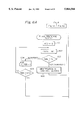
In FIG. 4 illustrates an embodiment of semiconductor device such as a CMOS LSI device including a plurality of logic blocks B1, B2, . . . Bz. Data input pins 1a of the semiconductor device 1 are supplied with a functional test pattern (FTP). The functional test pattern is generated by a memory 2, a timing generating circuit 3, a pattern generating circuit 4, a format controller 5, and PIN electronics units 61, 62, . . . connected to input pads of the semiconductor device 1.
The timing generating circuit 3 generates a timing signal for defining a test rate TO, a delay time TD and a pulse width Tw. Also, the timing generating circuit 3 generates a strobe signal STB and transmits it to a current detector 8 for detecting a quiescent VDD supply current Iqqd flowing from a power supply terminal VDD to a ground terminal GND in the semiconductor device 1.
The pattern generating circuit 4 generates a test pattern signal in accordance with data read out of the memory 2, which data is generally compressed.
Each of the PIN electronics units 61, 62, . . . is powered by voltages Vm and VL which are generated by digital/analog (D/A) converters 71 and 72, respectively. For example, when "0" is supplied to the PIN electronics unit 61, the voltage VL (=0V) is applied to the corresponding input pad. When "1" is supplied to the PIN electronics unit 61, the voltage VH is applied to the corresponding input pad.
The memory 2 receives an address signal SADD from a control circuit 9 which is comprised of a central processing unit (CPU), ROMs, RAMs, and the like. Therefore, if the content ADD of the address signal SADD is incremented by the control circuit 9, functional test patterns are sequentially generated and transmitted to the semiconductor device 1.
Simultaneously, the control circuit 9 monitors a quiescent VDD supply current Iqqd flowing through the semiconductor device 1 by the current detector 8.
Also, the control circuit 9 compares output data at data output pins 1b with expected data from the memory 2.
Further, connected to the control circuit 9 are an input apparatus 10 such as a keyboard or other controllers, and an output apparatus 11 such as a CRT.
Stored in the RAM of the control circuit 9 is a table showing a relationship between functional test patterns FTP (ADD) and operable blocks operated by the functional test patterns FTP (ADD) as shown in FIG. 5. Note that such blocks are designed by using application specific integrated circuit (ASIC) technology such as gate array technology, and therefore, the above-mentioned relationship can be recognized in advance.
FIGS. 6A and 6B show a first operation of the control circuit 9, FIG. 7 is a quiescent VDD supply current diagram for explaining the routine of FIG. 6, and FIG. 8 is a layout diagram for explaining the routine of FIG. 6.
First, at step 601, the address ADD is cleared.
Step 602 waits for a predetermined time period to pass, so that the semiconductor device 1 responds to the functional test pattern ETP of the address ADD to obtain a stable quiescent VDD supply current Iqqd. After the predetermined time has passed, the control proceeds to step 603.
At step 603, it is determined whether Iqqd >IR (definite value) is satisfied. If Iqqd ≦IR, which means that the quiescent VDD supply current Iqqd is normal, the control proceeds to steps 604 and 605. On the other hand, if Iqqd >IR, which means that the quiescent VDD supply current Iqqd is abnormal, the control proceeds to step 606.
Initially, as shown in FIG. 7, the quiescent VDD supply current Iqqd is usually normal (Iqqd ≦IR) Therefore, if Iqqd >IR at ADD=a as shown in FIG. 7, this means that the quiescent VDD supply current Iqqd is switched from normal to abnormal. Therefore, at step 606, transition blocks, which are the blocks which are not tested by between the functional test pattern FTP (a-1) but are tested by the functional test pattern FTP (a), are identified with reference to the table as shown in FIG. 5, since the fault point must exist in one or more of the transition blocks. In this case, the transition blocks are as shown in FIG. 8. Then, the control proceeds to step 607
At step 607, it is determined whether output data at the data output pins 1b are the same as the expected data stored in the memory 2. If the output data at the data output pins 1b are the same as the expected data, the control proceeds to steps 608, 609 and 610 which repeat the operation at step 607 until ADD reaches MAX. When ADD reaches MAX at step 609, the control proceeds via step 611 to step 615. Note that, at step 611, all the transition blocks identified at step 606 are deemed to include fault points.
On the other hand, if the output data are different from the expected data, at ADD=b as shown in FIG. 7, the control proceeds from step 607 to step 612.
At step 612, an abnormal data output pin which is an output pin which outputs data which does not conform to he expected data, such as Pb of the data output pins 1b as shown in FIG. 8 ,is identifined.
Next, at step 613, the output signals of the identified transition blocks are propagated or traced by a logic simulation or circuit arrangement infomation while the functional test patterns FTP (a), FTP (a+1), . . . , FTP (b-1) and FTP (b) as shown in FIG. 7 are sequentially applied to the semiconductor device 1.
Next, at step 614, a fault block is identified from among the identified transition blocks. That is, one or more of the transition blocks as shown in FIG. 8 whose output signals reached the data output pin Pb are identified as fault blocks. In FIG. 8, only one block is identified as a fault block; however, two or more blocks may be identified as fault blocks.
At step 615, the output signals of the fault blocks are defined to be "1" (high) or "0" (low). Then, the output signals of the fault blocks are propagated by a logic simulation or circuit arrangement infomation while the functional test patterns FTP (a), ETP (a+1), . . . , FTP (b-1) and FTP (b) are sequentially applied to the semiconductor device 1.
Next, at step 616, a similar identification process to that at step 614 is carried out. That is, only one fault block whose defined output signal reached the data output pin Pb may be identified.
Then, the routine of FIG. 6 is completed by step 617.
FIGS. 9A and 9B show a second operation of the control circuit 9, FIG. 10 is a quiescent VDD supply current diagram for explaining the routing of FIG. 9, and FIG. 11 is a layout diagram for explaining the routine of FIG. 6.
In FIG. 9, steps 901, 902 and 903 are provided instead of step 613 and 614 of FIG. 6.
The control at step 612 proceeds to step 901. At step 901, the output signal at the data output pin Pb as shown in FIG. 11 is fed back or traced by a logic simulation or circuit arrangement infomation while the functional test patterns FTP (b). FTP (b-1), . . . , FTP (a+1) and FTP (a) as shown in FIG. 10 are sequentially applied to the semiconductor device 1.
Next, at step 902, blocks related to the data output pin Pb as shown in FIG. 11 are identified.
Next, at step 903, a common block i.e., a block shared in common between the identified transition blocks and the blocks related to the data output pin Pb, is identified as a fault block. Also, in this case, in FIG. 11, only one block is identified as a fault block; however, two or more blocks may be identified as fault blocks.
Then, the control proceeds to step 615.
In FIGS. 12A and 12B, which illustrate a modification of the routine of FIG. 6, steps 1201 and 1202 are added to the routine of FIG. 6. As a result, the operation for identifying transition blocks at steps 603 and 606 and the operation for identifying fault blocks at steps 612 to 614 can be carried out by step 1201 a plurality of times. For example, as shown in FIG. 13, first fault blocks are identified by comparing transition blocks at FTP (a) and blocks related to an abnormal data output pin determined at ETP (b), second fault blocks are identified by comparing transition blocks at FTP (c) and blocks related to an abnormal data output pin determined at FTP (d), and third fault blocks are identified by comparing transition blocks at FTP (e) and blocks related to an abnormal data output pin determined at FTP (f). Next, at step 1202, common fault blocks among the first fault blocks, the second fault blocks and the third fault blocks are identified. In this case, the number of the common fault blocks is not larger than any one of the number of the first fault blocks, the number of second fault blocks or the number of third fault blocks.
In FIGS. 14A and 14B, which illustrate a modification of the routine of FIG. 9, steps 1401 and 1402 are added to the routine of FIG. 9. As a result, the operation for identifying transition blocks at steps 603 and 606 and the operation for identifying fault blocks at steps 612, 901 to 903 can be carried out by step 1401 a plurality of times. For example, as shown in FIG. 15, first fault blocks are identified from transition blocks at FTP (a) and blocks related to an abnormal data output pin determined at FTP (b), second fault blocks are identified from transition blocks at FTP (c) and blocks related to an abnormal data output pin determined at FTP (d), and third fault blocks are identified from transition blocks at FTP (e) and blocks related to an abnormal data output pin determined at FTP (f). Next, at step 1402, common fault blocks among the first fault blocks, the second fault blocks and the third fault blocks are identified. In this case, the number of common the fault blocks is not larger than any one of the number of first fault blocks, the number of second fault blocks or the number of third fault blocks.
In FIGS. 16A and 16B, which illustrate another modification of the routine of FIG. 6, steps 1601 and 1602 are added to the routine of FIG. 6. As a result, only the operation for identifying fault blocks at steps 612 to 614 can be carried out by step 1601 a plurality of times, although the operation for identifying transition blocks at steps 603 and 606 is carried out only once.
For example, as shown in FIG. 17, the quiescent VDD supply current Iddq is abnormal at ETP (a), and data at the data output pins Pb, Pc, Pd, Pe and Pf are abnormal at FTP (b), FTP (c), FTP (d), FTP (e) and FTP (f), respectively.
Then, as shown in FIG. 18, first fault blocks B are identified from the transition blocks at FTP (a) and blocks related to the data output pin Pb determined at FTP (b), second fault blocks C are identified from the transition blocks at FTP (a) and blocks related to the data output pin Pc determined at FTP (c), third fault blocks D are identified from the transition blocks at FTP (a) and blocks related to the data output pin Pd determined at FTP (d), fourth fault blocks E are identified from the transition blocks at FTP (a) and blocks related to the data output pin Pe determined at FTP (e), fifth fault blocks F are identified from the transition blocks at FTP (a) and blocks related to the data output pin Pf determined at FTP (f). Next, at step 1602, common fault blocks among the first fault blocks, the second fault blocks, the third fault blocks, the fourth fault blocks and the fifth fault blocks are identified. In this case, the number of the common fault blocks is not larger than any one of the number of first fault blocks, the number of second fault blocks, the number of third fault blocks, the number of fourth fault blocks or the number of fifth fault blocks.
In FIGS. 19A and 19B, which illustrate another modification of the routine of FIG. 9, steps 1901 and 1902 are added to the routine of FIG. 6. As a result, only the operation for identifying fault blocks at steps 612, 901 to 614 can be carried out by step 1901 at a plurality of times, although the operation for identifying transition blocks at steps 603 and 606 is carried out only once.
For example, as shown in FIG. 20, the quiescent VDD supply current Iqqd is abnormal at FTP (a), and data at the data output pins Pb, Pc, Pd, Pe and Pf are abnormal at FTP (b), FTP (c), FTP (d), FTP (e) and FTP (f), respectively.
Then, as shown in FIG. 21, first fault blocks B are identified from the transition blocks at FTP (a) and blocks related to the data output pin Pb determined at FTP (b), second fault blocks C are identified from the transition blocks at FTP (a) and blocks related to the data output pin Pc determined at FTP (c), third fault blocks D are identified from the transition blocks at FTP (a) and blocks related to the data output pin Pd determined at ETP (b), fourth fault blocks E are identified from the transition blocks at FTP (a) and blocks related to the data output pin Pe determined at FTP (e), and fifth fault blocks F are identified from the transition blocks at FTP (a) and blocks related to the data output pin Pf determined at FTP (f). Next, at step 1902, common fault blocks among the first fault blocks, the second fault blocks, the third fault blocks, the fourth fault blocks and the fifth fault blocks are identified. In this case, the number of common fault blocks is not larger than any one of the number of first fault blocks, the number of second fault blocks, the number of third fault blocks, the number of fourth fault blocks or the number of fifth fault blocks.
The present invention can be applied to a hierarchic testing system as illustrated in FIGS. 22A, 22B and 22C. First, one of the above-described operations is applied to a semiconductor device which is divided into a plurality of large blocks as illustrated in FIG. 22A, so that a fault block X is found. Next, one of the above-described operations is applied to the fault block X which is sub-divided into a plurality of small blocks as illustrated in FIG. 22B, so that a fault sub-block Y is found. Finally, a logic simulation is carried out to find a basic logic circuit Z such as a NOR circuit as a fault point as illustrated in FIG. 22C.
As explained hereinbefore, according to the present invention, since a fault block within a semiconductor device is determined by using a quiescent VDD supply current in response to functional test patterns and an abnormal data at data output pins, a fault point within the semiconductor device, i.e., a fault point within the fault block can be detected without using a large fault dictionary.
Claims (6)
1. A system for detecting a fault block in a semiconductor device having a plurality of logic blocks, comprising: a table means for storing a plurality of functional test patterns and associated expected output patterns of operable logic circuits of said logic blocks produced upon application of said functional test patterns thereto;
means for sequentially applying said functional test patterns to said semiconductor device;
means for identifying, in accordance with said table, transition blocks from among said logic blocks associated with an i-th functional test pattern when application of said i-th functional test pattern to said semiconductor device produces a supply current in said semiconductor device which exceeds a predetermined value;
means for identifying, as an abnormal data output pin associated with a j-th functional test pattern, a data output pin having an output which is different from an expected output of said pin associated with said j-th functional test pattern when said j-th functional test pattern is applied to said semiconductor device;
means for sequentially tracing output signals of said transition blocks upon application of functional test patterns beginning with said i-th functional test pattern and ending with said j-th functional test pattern; and
means for identifying as fault blocks transition blocks associated with said i-th functional test pattern whose output signals produce output at an abnormal data output pin associated with said j-th functional test pattern.
2. The system as set forth in claim 1, further comprising:
means for repeating operations of said means for sequentially applying said patterns, said means for identifying transition blocks, said means for identifying a data output pin, said means for sequentially tracing, and said means for identifying fault blocks; and
means for identifying common fault blocks from among fault blocks identified by said means for identifying fault blocks.
3. The system as set forth in claim 1, further comprising:
means for repeating operations of said means for identifying a data output pin, said means for sequentially tracing, and said means for identifying fault blocks; and
means for identifying at least one common fault block from among fault blocks identified by said means for identifying fault blocks.
4. A system for detecting a fault block in a semiconductor device having a plurality of logic blocks, comprising:
a table means for storing a plurality of functional test patterns and associated expected output patterns of operable logic circuits of said logic blocks produced upon application of said functional test patterns thereto;
means for sequentially applying said functional test patterns to said semiconductor device;
means for identifying, in accordance with said table, transition blocks from among said logic blocks associated with an i-th functional test pattern when application of said i-th functional test pattern to said semiconductor device produces a supply current in said semiconductor device which exceeds a predetermined value;
means for identifying, as an abnormal data output pin associated with a j-th functional test pattern, a data output pin having an output which is different from an expected output of said pin associated with said j-th functional test pattern when said j-th functional test pattern is applied to said semiconductor device;
means for feeding back signals of an abnormal data output pin by sequentially applying said functional test patterns to said semiconductor device beginning with said i-th functional test pattern and ending with said i-th functional test pattern; and
means for identifying, from among said transition blocks associated with said i-th functional test pattern, fault blocks at which the signals of abnormal data output pins associated with said j-th functional test pattern have arrived through action of said means for feeding back signals.
5. The system as set forth in claim 4, further comprising:
means for repeating operations of said means for sequentially applying functional test patterns, said means for identifying transition blocks, said means for identifying an abnormal data output pin, said means for feeding back, and said means for identifying fault blocks; and
means for identifying at least one common fault block from among fault blocks identified by said means for identifying fault blocks.
6. The system as set forth in claim 4, further comprising:
means for repeating operations of said means for identifying abnormal data output pins, said means for feeding back, and said means for identifying fault blocks; and
means for identifying at least one common fault block from among fault blocks identified by said means for identifying fault blocks.
Priority Applications (1)
| Application Number | Priority Date | Filing Date | Title |
|---|---|---|---|
| US08/970,537 US5864566A (en) | 1995-03-10 | 1997-11-14 | Fault block detecting system using abnormal current and abnormal data output |
Applications Claiming Priority (7)
| Application Number | Priority Date | Filing Date | Title |
|---|---|---|---|
| JP7-051590 | 1995-03-10 | ||
| JP7051590A JP2715963B2 (en) | 1995-03-10 | 1995-03-10 | How to narrow down faults in logic circuits |
| JP7129769A JP2715989B2 (en) | 1995-04-28 | 1995-04-28 | Method for narrowing down a failure portion of CMOS logic circuit using Iddq |
| JP7-129769 | 1995-04-28 | ||
| US61282596A | 1996-03-11 | 1996-03-11 | |
| US86178297A | 1997-05-22 | 1997-05-22 | |
| US08/970,537 US5864566A (en) | 1995-03-10 | 1997-11-14 | Fault block detecting system using abnormal current and abnormal data output |
Related Parent Applications (1)
| Application Number | Title | Priority Date | Filing Date |
|---|---|---|---|
| US86178297A Continuation | 1995-03-10 | 1997-05-22 |
Publications (1)
| Publication Number | Publication Date |
|---|---|
| US5864566A true US5864566A (en) | 1999-01-26 |
Family
ID=26392132
Family Applications (1)
| Application Number | Title | Priority Date | Filing Date |
|---|---|---|---|
| US08/970,537 Expired - Fee Related US5864566A (en) | 1995-03-10 | 1997-11-14 | Fault block detecting system using abnormal current and abnormal data output |
Country Status (3)
| Country | Link |
|---|---|
| US (1) | US5864566A (en) |
| KR (1) | KR100204852B1 (en) |
| DE (1) | DE19609085A1 (en) |
Cited By (4)
| Publication number | Priority date | Publication date | Assignee | Title |
|---|---|---|---|---|
| US6173426B1 (en) * | 1997-02-24 | 2001-01-09 | Nec Corporation | Method of locating faults in LSI |
| US6476631B1 (en) * | 2001-06-29 | 2002-11-05 | Lsi Logic Corporation | Defect screening using delta VDD |
| US20040163023A1 (en) * | 2000-04-04 | 2004-08-19 | Masahiro Ishida | Method and apparatus for defect analysis of semiconductor integrated circuit |
| US20100131811A1 (en) * | 2008-11-27 | 2010-05-27 | Nec Electronics Corporation | Semiconductor device and verify method for semiconductor device |
Citations (3)
| Publication number | Priority date | Publication date | Assignee | Title |
|---|---|---|---|---|
| US5321354A (en) * | 1990-07-23 | 1994-06-14 | Seiko Epson Corporation | Method for inspecting semiconductor devices |
| US5392283A (en) * | 1993-08-27 | 1995-02-21 | Motorola, Inc. | Data communication protocol |
| US5449960A (en) * | 1992-03-30 | 1995-09-12 | Nec Corporation | Sample-and-hold circuit |
Family Cites Families (3)
| Publication number | Priority date | Publication date | Assignee | Title |
|---|---|---|---|---|
| DE4117493A1 (en) * | 1991-05-28 | 1992-12-03 | Guenter Kemnitz | Controlling quiescent power supply current test for CMOS circuits - applying test steps to stimulate circuit being tested with changeover operations releasing input signals when test set is completed |
| DE4305288A1 (en) * | 1993-02-20 | 1994-08-25 | Bosch Gmbh Robert | Self-test procedure for non-regular CMOS switching structures with high defect detection |
| US5392293A (en) * | 1993-02-26 | 1995-02-21 | At&T Corp. | Built-in current sensor for IDDQ testing |
-
1996
- 1996-03-08 DE DE19609085A patent/DE19609085A1/en not_active Withdrawn
- 1996-03-09 KR KR1019960006233A patent/KR100204852B1/en not_active Expired - Fee Related
-
1997
- 1997-11-14 US US08/970,537 patent/US5864566A/en not_active Expired - Fee Related
Patent Citations (4)
| Publication number | Priority date | Publication date | Assignee | Title |
|---|---|---|---|---|
| US5321354A (en) * | 1990-07-23 | 1994-06-14 | Seiko Epson Corporation | Method for inspecting semiconductor devices |
| US5449960A (en) * | 1992-03-30 | 1995-09-12 | Nec Corporation | Sample-and-hold circuit |
| US5467035A (en) * | 1992-03-30 | 1995-11-14 | Nec Corporation | Sample-and-hold circuit |
| US5392283A (en) * | 1993-08-27 | 1995-02-21 | Motorola, Inc. | Data communication protocol |
Non-Patent Citations (4)
| Title |
|---|
| M. Sanada, "Evalution and Detection of CMOS-LSI with Abnormal IDD2", Microelectron. Reliab., vol. 35, No. 3, pp. 619-629, 1995. |
| M. Sanada, "New Applicaton of Laser Beam to Failure Analysis of LSI with Multi-Metal Layers", Microelectron. Reliab., vol. 33, No. 7, pp. 993-1009, 1993. |
| M. Sanada, Evalution and Detection of CMOS LSI with Abnormal IDD2 , Microelectron. Reliab., vol. 35, No. 3, pp. 619 629, 1995. * |
| M. Sanada, New Applicaton of Laser Beam to Failure Analysis of LSI with Multi Metal Layers , Microelectron. Reliab., vol. 33, No. 7, pp. 993 1009, 1993. * |
Cited By (5)
| Publication number | Priority date | Publication date | Assignee | Title |
|---|---|---|---|---|
| US6173426B1 (en) * | 1997-02-24 | 2001-01-09 | Nec Corporation | Method of locating faults in LSI |
| US20040163023A1 (en) * | 2000-04-04 | 2004-08-19 | Masahiro Ishida | Method and apparatus for defect analysis of semiconductor integrated circuit |
| US6476631B1 (en) * | 2001-06-29 | 2002-11-05 | Lsi Logic Corporation | Defect screening using delta VDD |
| US20100131811A1 (en) * | 2008-11-27 | 2010-05-27 | Nec Electronics Corporation | Semiconductor device and verify method for semiconductor device |
| US8042013B2 (en) * | 2008-11-27 | 2011-10-18 | Renesas Electronics Corporation | Semiconductor device and verify method for semiconductor device |
Also Published As
| Publication number | Publication date |
|---|---|
| KR960035043A (en) | 1996-10-24 |
| DE19609085A1 (en) | 1996-09-12 |
| KR100204852B1 (en) | 1999-06-15 |
Similar Documents
| Publication | Publication Date | Title |
|---|---|---|
| EP0494311A1 (en) | Method of inspecting semiconductor device, apparatus for inspecting the same, and method of manufacturing the same | |
| US4720818A (en) | Semiconductor memory device adapted to carry out operation test | |
| KR950009740A (en) | Apparatus and method for testing static rams | |
| JPH0481147B2 (en) | ||
| US7519486B2 (en) | Method and apparatus to test the power-on-reset trip point of an integrated circuit | |
| US4980889A (en) | Multi-mode testing systems | |
| US5850404A (en) | Fault block detecting system using abnormal current | |
| US5864566A (en) | Fault block detecting system using abnormal current and abnormal data output | |
| US5796260A (en) | Parametric test circuit | |
| US5225774A (en) | Semiconductor integrated circuit | |
| US6519726B1 (en) | Semiconductor device and testing method of the same | |
| JP2728233B2 (en) | Semiconductor logic circuit | |
| KR100311972B1 (en) | Generation circuit of mode signal in semiconductor memory device | |
| JP3980560B2 (en) | Testable cascode circuit and method for testing the same | |
| US7639036B2 (en) | Semiconductor integrated circuit | |
| US6130851A (en) | Semiconductor memory having a redundancy fuse broken by an electric current | |
| JP2848441B2 (en) | CMOS semiconductor device | |
| US7418637B2 (en) | Methods and apparatus for testing integrated circuits | |
| KR100546276B1 (en) | Input buffer and input buffer control method of semiconductor memory device | |
| KR0147632B1 (en) | Multibit testing method and test circuit of semiconductor device | |
| KR100238866B1 (en) | Array vcc generator being used in burn-in testing operation | |
| KR100194201B1 (en) | Test circuit of semiconductor memory device | |
| JP3395773B2 (en) | Semiconductor device | |
| JP2006078289A (en) | Semiconductor memory device and test method thereof | |
| Hwang | Design-for-testability schemes for detecting multiple faults in CMOS integrated circuits |
Legal Events
| Date | Code | Title | Description |
|---|---|---|---|
| FEPP | Fee payment procedure |
Free format text: PAYOR NUMBER ASSIGNED (ORIGINAL EVENT CODE: ASPN); ENTITY STATUS OF PATENT OWNER: LARGE ENTITY |
|
| FPAY | Fee payment |
Year of fee payment: 4 |
|
| REMI | Maintenance fee reminder mailed | ||
| LAPS | Lapse for failure to pay maintenance fees | ||
| STCH | Information on status: patent discontinuation |
Free format text: PATENT EXPIRED DUE TO NONPAYMENT OF MAINTENANCE FEES UNDER 37 CFR 1.362 |
|
| FP | Lapsed due to failure to pay maintenance fee |
Effective date: 20070126 |