US5854109A - Silicide process for manufacturing a mask ROM - Google Patents
Silicide process for manufacturing a mask ROM Download PDFInfo
- Publication number
- US5854109A US5854109A US08/863,626 US86362697A US5854109A US 5854109 A US5854109 A US 5854109A US 86362697 A US86362697 A US 86362697A US 5854109 A US5854109 A US 5854109A
- Authority
- US
- United States
- Prior art keywords
- forming
- layer
- process according
- silicon substrate
- polysilicon
- Prior art date
- Legal status (The legal status is an assumption and is not a legal conclusion. Google has not performed a legal analysis and makes no representation as to the accuracy of the status listed.)
- Expired - Lifetime
Links
- 238000000034 method Methods 0.000 title claims abstract description 32
- 229910021332 silicide Inorganic materials 0.000 title claims abstract description 6
- FVBUAEGBCNSCDD-UHFFFAOYSA-N silicide(4-) Chemical compound [Si-4] FVBUAEGBCNSCDD-UHFFFAOYSA-N 0.000 title claims abstract description 6
- 238000004519 manufacturing process Methods 0.000 title description 4
- 229910021420 polycrystalline silicon Inorganic materials 0.000 claims description 29
- 229920005591 polysilicon Polymers 0.000 claims description 29
- 239000000758 substrate Substances 0.000 claims description 20
- XUIMIQQOPSSXEZ-UHFFFAOYSA-N Silicon Chemical compound [Si] XUIMIQQOPSSXEZ-UHFFFAOYSA-N 0.000 claims description 14
- 229910052710 silicon Inorganic materials 0.000 claims description 14
- 239000010703 silicon Substances 0.000 claims description 14
- 150000002500 ions Chemical class 0.000 claims description 10
- 238000005530 etching Methods 0.000 claims description 8
- 125000006850 spacer group Chemical group 0.000 claims description 7
- RTAQQCXQSZGOHL-UHFFFAOYSA-N Titanium Chemical compound [Ti] RTAQQCXQSZGOHL-UHFFFAOYSA-N 0.000 claims description 4
- 229910052719 titanium Inorganic materials 0.000 claims description 4
- 239000010936 titanium Substances 0.000 claims description 4
- 238000001039 wet etching Methods 0.000 claims description 4
- 238000004140 cleaning Methods 0.000 claims description 2
- 238000000151 deposition Methods 0.000 claims description 2
- 238000004544 sputter deposition Methods 0.000 claims description 2
- 230000015572 biosynthetic process Effects 0.000 abstract 1
- 239000004065 semiconductor Substances 0.000 description 6
- 238000005229 chemical vapour deposition Methods 0.000 description 2
- 239000012535 impurity Substances 0.000 description 2
- 238000012986 modification Methods 0.000 description 2
- 230000004048 modification Effects 0.000 description 2
- UGACIEPFGXRWCH-UHFFFAOYSA-N [Si].[Ti] Chemical group [Si].[Ti] UGACIEPFGXRWCH-UHFFFAOYSA-N 0.000 description 1
- 230000002411 adverse Effects 0.000 description 1
- 238000007796 conventional method Methods 0.000 description 1
- 230000003247 decreasing effect Effects 0.000 description 1
- 238000010586 diagram Methods 0.000 description 1
- 230000000694 effects Effects 0.000 description 1
- 238000005516 engineering process Methods 0.000 description 1
- 239000007943 implant Substances 0.000 description 1
- 239000000463 material Substances 0.000 description 1
- 230000003647 oxidation Effects 0.000 description 1
- 238000007254 oxidation reaction Methods 0.000 description 1
- 229920002120 photoresistant polymer Polymers 0.000 description 1
- 229910021341 titanium silicide Inorganic materials 0.000 description 1
Images


Classifications
-
- H—ELECTRICITY
- H10—SEMICONDUCTOR DEVICES; ELECTRIC SOLID-STATE DEVICES NOT OTHERWISE PROVIDED FOR
- H10B—ELECTRONIC MEMORY DEVICES
- H10B20/00—Read-only memory [ROM] devices
- H10B20/27—ROM only
- H10B20/30—ROM only having the source region and the drain region on the same level, e.g. lateral transistors
- H10B20/38—Doping programmed, e.g. mask ROM
-
- H—ELECTRICITY
- H10—SEMICONDUCTOR DEVICES; ELECTRIC SOLID-STATE DEVICES NOT OTHERWISE PROVIDED FOR
- H10B—ELECTRONIC MEMORY DEVICES
- H10B20/00—Read-only memory [ROM] devices
Definitions
- This invention relates in general to a method of making read-only-memories (ROMs), and more particularly to a self-aligned silicide (SALICIDE) process used for making a mask ROM.
- ROMs read-only-memories
- SALICIDE self-aligned silicide
- ROM devices utilize channel transistors as a basic memory unit.
- impurities are selectively implanted into designated channel regions so as to adjust the threshold voltage, thus setting each memory unit to either an ON state or an OFF state.
- FIG. 1 is a top view showing a conventional mask ROM.
- the conventional mask ROM is formed by doping N-type ions into a P-doped silicon substrate 100 to form N + source/drain regions 104 extending in a first direction 110 and which serve as bit lines.
- gate electrodes 106 are formed above a gate oxide layer (not shown in the figure) that covers the silicon substrate 100.
- the gate electrodes 106 extend in a second direction 120 and act as word lines.
- the first direction 110 is perpendicular to the second direction 120.
- a transistor channel is formed underneath the word line and between two adjacent bit lines.
- P-type impurities are implanted into designated channels, for example, channel 108 in FIG. 1, thus raising its threshold voltage. This is known as a coding implant.
- the aforementioned conventional ROM device will have a higher word line resistance when its line width is decreased due to component miniaturization. This will have an adverse effect on its operational speed, and hence will lower its component quality.
- the salicide process for a mask ROM involves forming a gate oxide layer and a first polysilicon layer sequentially above a silicon substrate. Photolithographic and etching processes are used to pattern the first polysilicon layer, and form a number of separate long polysilicon strips along a first direction. Ions are implanted into the silicon substrate not covered by the long polysilicon strips, to form a number of bit lines. A second polysilicon layer is formed above the silicon substrate, and covers both the long polysilicon strips as well as the bit lines. Photolithographic and etching processes are used to pattern the second polysilicon layer and the long polysilicon strips, and form a number of word lines along a second direction, that are perpendicular to the first direction. Spacers are formed on the sidewalls of the word lines. A metallic layer is formed above the silicon substrate. Then a high temperature is applied, and wet etching is performed to form a salicide layer above the bit lines and the word lines.
- FIG. 1 is a top view of a conventional mask ROM
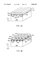
- FIGS. 2A through 2F are a series of diagrams showing the processing flow of a salicide layer in a mask ROM according to this invention.
- FIG. 3 is a table comparing the conventional resistance values of word lines and bit lines with those manufactured according to the present invention.
- a semiconductor substrate 200 doped with a first type of ions for example, a P-doped silicon substrate.
- the substrate 200 has a gate oxide layer 202 and a first polysilicon layer 204 sequentially formed thereabove.
- the gate oxide layer 202 can be formed using, for example, a thermal oxidation method or a chemical vapor deposition (CVD) method.
- the thickness of the first polysilicon layer 204 is about 300 ⁇ to about 500 ⁇ .
- a photolithographic process is used to define a pattern on the semiconductor substrate 200.
- a second type of ions 208 for example, N + ions, is implanted into the semiconductor substrate 200 through a portion of the surface not covered by a photoresist layer (not shown in the Figure).
- part of the first polysilicon layer 204 is etched away to form a number of long separate polysilicon strips 204a which extend in a first direction 210, and a number of N + ion doped bit lines 206 which likewise extend in direction 210.
- a second polysilicon layer 212 is formed above the semiconductor substrate 200, which covers the polysilicon strips 204a and the bit lines 206.
- photolithographic and etching processes are used to pattern and remove a portion of the second polysilicon layer 212 and the polysilicon strips 204a, thereby forming a number of separate word lines 212a extending in a second direction 220.
- the second direction 220 is perpendicular to the first direction 210. Since the bit lines 206 are protected only by the second polysilicon layer 212 thereabove, during the process of removing the polysilicon strips 204a, the portion of the gate oxide layer 202 above the bit lines 206, as well as portions of the bit lines 206 themselves, will also be removed. The extent to which the bit lines 206 are removed during etching can be controlled through adjusting a thickness of the first polysilicon layer 204.
- spacers 214 are formed on the sidewalls of each word line 212a.
- the spacers 214 are formed, for example, by depositing an insulating layer (not shown in the figure) above the semiconductor substrate 200, and then etching back the insulating layer.
- a titanium layer is formed over the bit lines 206, the spacers 214, and the word lines 212a using, for example, a sputtering method.
- the titanium layer has a thickness of about 300 ⁇ to about 400 ⁇ .
- a rapid thermal processing (RTP) operation is performed at a temperature of 620° C. for a duration of about 30 seconds, and at a temperature of 750° C. for a duration of about 30 seconds.
- a portion of the deposited titanium layer is allowed to react with the polysilicon in the bit lines 206 and the word lines 212a, thus forming a C-49 phase titanium silicide (TiSI) structure.
- a wet etching procedure is used to remove any unreacted and residual material.
- This procedure is preferably an RCA cleaning operation.
- an RTP operation is again performed using a temperature of about 825° C. for about 20 seconds to form a C-54 phase titanium silicide layer structure 216, which has a lower resistance on the surface of bit lines 206 and word lines 212a.
- Table 1 lists the resistance values of the bit lines 206 and the word lines 212a obtained using a conventional method versus the method according to this invention. As can be seen, there is a significant decrease in the resistance values when the method of this invention is used.
Landscapes
- Semiconductor Memories (AREA)
Abstract
Description
Claims (10)
Applications Claiming Priority (2)
| Application Number | Priority Date | Filing Date | Title |
|---|---|---|---|
| TW086104371A TW340966B (en) | 1997-04-07 | 1997-04-07 | The salicide process for mask ROM |
| TW86104371 | 1997-04-07 |
Publications (1)
| Publication Number | Publication Date |
|---|---|
| US5854109A true US5854109A (en) | 1998-12-29 |
Family
ID=21626519
Family Applications (1)
| Application Number | Title | Priority Date | Filing Date |
|---|---|---|---|
| US08/863,626 Expired - Lifetime US5854109A (en) | 1997-04-07 | 1997-05-27 | Silicide process for manufacturing a mask ROM |
Country Status (2)
| Country | Link |
|---|---|
| US (1) | US5854109A (en) |
| TW (1) | TW340966B (en) |
Cited By (7)
| Publication number | Priority date | Publication date | Assignee | Title |
|---|---|---|---|---|
| US6372580B1 (en) | 2000-03-15 | 2002-04-16 | Winbond Electronics Corp. | Process for making mask ROM using a salicide process and mask ROM |
| US20030124777A1 (en) * | 2001-12-26 | 2003-07-03 | Kim Seok Su | Method of fabricating mask ROM |
| US6720210B1 (en) * | 2002-10-17 | 2004-04-13 | Macronix International Co., Ltd | Mask ROM structure and manufacturing method thereof |
| US20060228882A1 (en) * | 2005-04-07 | 2006-10-12 | Magnachip Semiconductor, Ltd. | Method for fabricating semiconductor device |
| US7442610B2 (en) * | 2002-05-06 | 2008-10-28 | Macronix International Co., Ltd. | Low thermal budget fabrication method for a mask read only memory device |
| CN102810516A (en) * | 2011-06-02 | 2012-12-05 | 无锡华润上华半导体有限公司 | ROM (read only memory) device and manufacturing method thereof |
| NL1042970A (en) * | 2017-08-28 | 2019-03-07 | Mapper Lithography Ip Bv | Memory device with predetermined start-up value |
Citations (5)
| Publication number | Priority date | Publication date | Assignee | Title |
|---|---|---|---|---|
| US5362662A (en) * | 1989-08-11 | 1994-11-08 | Ricoh Company, Ltd. | Method for producing semiconductor memory device having a planar cell structure |
| US5384478A (en) * | 1993-07-28 | 1995-01-24 | United Microelectronics Corporation | Mask ROM process |
| US5504025A (en) * | 1994-05-18 | 1996-04-02 | United Microelectronics Corp. | Method of fabricating a read-only memory cell configuration having steep trenches |
| US5648289A (en) * | 1994-06-30 | 1997-07-15 | Lg Semicon Co., Ltd. | Method for coding semiconductor read only memory device |
| US5688661A (en) * | 1995-12-30 | 1997-11-18 | Lg Semicon Co., Ltd. | Fabrication method for mask ROM |
-
1997
- 1997-04-07 TW TW086104371A patent/TW340966B/en not_active IP Right Cessation
- 1997-05-27 US US08/863,626 patent/US5854109A/en not_active Expired - Lifetime
Patent Citations (5)
| Publication number | Priority date | Publication date | Assignee | Title |
|---|---|---|---|---|
| US5362662A (en) * | 1989-08-11 | 1994-11-08 | Ricoh Company, Ltd. | Method for producing semiconductor memory device having a planar cell structure |
| US5384478A (en) * | 1993-07-28 | 1995-01-24 | United Microelectronics Corporation | Mask ROM process |
| US5504025A (en) * | 1994-05-18 | 1996-04-02 | United Microelectronics Corp. | Method of fabricating a read-only memory cell configuration having steep trenches |
| US5648289A (en) * | 1994-06-30 | 1997-07-15 | Lg Semicon Co., Ltd. | Method for coding semiconductor read only memory device |
| US5688661A (en) * | 1995-12-30 | 1997-11-18 | Lg Semicon Co., Ltd. | Fabrication method for mask ROM |
Cited By (14)
| Publication number | Priority date | Publication date | Assignee | Title |
|---|---|---|---|---|
| US6372580B1 (en) | 2000-03-15 | 2002-04-16 | Winbond Electronics Corp. | Process for making mask ROM using a salicide process and mask ROM |
| US20020094645A1 (en) * | 2000-03-15 | 2002-07-18 | Jiann-Ming Shiau | Process for making mask ROM using a salicide process and mask ROM |
| US6894333B2 (en) * | 2000-03-15 | 2005-05-17 | Winbond Electronics Corporation | Oxide layer of variable thickness between word lines and bit lines of a memory device |
| US6709933B2 (en) | 2001-12-26 | 2004-03-23 | Dongbu Electronics Co., Ltd. | Method of fabricating mask ROM |
| US20030124777A1 (en) * | 2001-12-26 | 2003-07-03 | Kim Seok Su | Method of fabricating mask ROM |
| US7442610B2 (en) * | 2002-05-06 | 2008-10-28 | Macronix International Co., Ltd. | Low thermal budget fabrication method for a mask read only memory device |
| US6720210B1 (en) * | 2002-10-17 | 2004-04-13 | Macronix International Co., Ltd | Mask ROM structure and manufacturing method thereof |
| US20040077131A1 (en) * | 2002-10-17 | 2004-04-22 | Ching-Yu Chang | Mask rom structure and manufacturing method thereof |
| US20060228882A1 (en) * | 2005-04-07 | 2006-10-12 | Magnachip Semiconductor, Ltd. | Method for fabricating semiconductor device |
| US7364963B2 (en) | 2005-04-07 | 2008-04-29 | Magnachip Semiconductor, Ltd. | Method for fabricating semiconductor device |
| CN102810516A (en) * | 2011-06-02 | 2012-12-05 | 无锡华润上华半导体有限公司 | ROM (read only memory) device and manufacturing method thereof |
| CN102810516B (en) * | 2011-06-02 | 2015-02-04 | 无锡华润上华半导体有限公司 | ROM (read only memory) device and manufacturing method thereof |
| NL1042970A (en) * | 2017-08-28 | 2019-03-07 | Mapper Lithography Ip Bv | Memory device with predetermined start-up value |
| US11501952B2 (en) | 2017-08-28 | 2022-11-15 | Asml Netherlands B.V. | Memory device with predetermined start-up value |
Also Published As
| Publication number | Publication date |
|---|---|
| TW340966B (en) | 1998-09-21 |
Similar Documents
| Publication | Publication Date | Title |
|---|---|---|
| US7348636B2 (en) | CMOS transistor having different PMOS and NMOS gate electrode structures and method of fabrication thereof | |
| US6287907B1 (en) | Method of manufacturing a flash memory having a select transistor | |
| US6821887B2 (en) | Method of forming a metal silicide gate in a standard MOS process sequence | |
| US6630721B1 (en) | Polysilicon sidewall with silicide formation to produce high performance MOSFETS | |
| US6159795A (en) | Low voltage junction and high voltage junction optimization for flash memory | |
| KR980011938A (en) | A method of making self-aligned polysides using a planarized layer of material to expose a polysilicon structure to sequentially deposited metal layers reacted to form metal silicides | |
| KR20040075021A (en) | Monos device having buried metal silicide bit line | |
| US6423634B1 (en) | Method of forming low resistance metal silicide region on a gate electrode of a transistor | |
| US5854109A (en) | Silicide process for manufacturing a mask ROM | |
| US7217657B2 (en) | Semiconductor device having different metal silicide portions and method for fabricating the semiconductor device | |
| US5550073A (en) | Method for manufacturing an EEPROM cell | |
| EP1093667B1 (en) | Method of manufacturing a semiconductor device comprising a field effect transistor | |
| JP2005519468A (en) | Method for forming different silicide portions on different silicon-containing regions in a semiconductor device | |
| US6194296B1 (en) | Method for making planarized polycide | |
| KR20000042407A (en) | Method of manufacturing polycide gate electrode of semiconductor device | |
| EP1479100A1 (en) | Method for fabricating a semiconductor device having different metal silicide portions | |
| US6674135B1 (en) | Semiconductor structure having elevated salicided source/drain regions and metal gate electrode on nitride/oxide dielectric | |
| KR100602121B1 (en) | Manufacturing method of semiconductor device | |
| EP1017088A1 (en) | Selective salicization process for semiconductor devices | |
| KR20000041468A (en) | Method of forming polycide gate electrode by using silicon film of amorphous phase | |
| KR100437620B1 (en) | Method for forming polycide structure of semiconductor device | |
| KR100255136B1 (en) | Gate electrode of semiconductor device and method for manufacturing the same | |
| KR100318260B1 (en) | Manufacturing method of semiconductor device | |
| KR100542246B1 (en) | Manufacturing method of MOSFET consisting of polyside gate electrode | |
| KR20000025633A (en) | Method for forming contact of semiconductor device |
Legal Events
| Date | Code | Title | Description |
|---|---|---|---|
| AS | Assignment |
Owner name: UNITED MICROELECTRONICS CORP., TAIWAN Free format text: ASSIGNMENT OF ASSIGNORS INTEREST;ASSIGNORS:SHENG, YI-CHUNG;CHUNG, CHENG-HUI;REEL/FRAME:008583/0261 Effective date: 19970509 |
|
| STCF | Information on status: patent grant |
Free format text: PATENTED CASE |
|
| FEPP | Fee payment procedure |
Free format text: PAYER NUMBER DE-ASSIGNED (ORIGINAL EVENT CODE: RMPN); ENTITY STATUS OF PATENT OWNER: LARGE ENTITY Free format text: PAYOR NUMBER ASSIGNED (ORIGINAL EVENT CODE: ASPN); ENTITY STATUS OF PATENT OWNER: LARGE ENTITY |
|
| FPAY | Fee payment |
Year of fee payment: 4 |
|
| FPAY | Fee payment |
Year of fee payment: 8 |
|
| FPAY | Fee payment |
Year of fee payment: 12 |