US5825212A - High speed single ended bit line sense amplifier - Google Patents
High speed single ended bit line sense amplifier Download PDFInfo
- Publication number
- US5825212A US5825212A US08/698,343 US69834396A US5825212A US 5825212 A US5825212 A US 5825212A US 69834396 A US69834396 A US 69834396A US 5825212 A US5825212 A US 5825212A
- Authority
- US
- United States
- Prior art keywords
- bit line
- ended bit
- voltage
- line input
- input
- Prior art date
- Legal status (The legal status is an assumption and is not a legal conclusion. Google has not performed a legal analysis and makes no representation as to the accuracy of the status listed.)
- Expired - Lifetime
Links
Images


Classifications
-
- G—PHYSICS
- G11—INFORMATION STORAGE
- G11C—STATIC STORES
- G11C7/00—Arrangements for writing information into, or reading information out from, a digital store
- G11C7/06—Sense amplifiers; Associated circuits, e.g. timing or triggering circuits
- G11C7/067—Single-ended amplifiers
Definitions
- the present invention relates to semiconductor memory devices and, in particular, to a single ended bit line sense amplifier.
- a semiconductor memory device has a plurality of output "bit lines", with each line having a logic state that is indicative of the data being read from the memory device.
- the output bit lines are either single ended or differential.
- a single ended bit line is typically precharged high or low (most often high). During a read operation, the precharge on the bit line is removed and the bit line will then either stay high or fall low, depending upon the data on the bit line.
- a sense amplifier senses the logic state on the bit line.
- a traditional sense amplifier includes an inverter coupled in series with the bit line.
- a typical CMOS inverter includes an N-channel and a P-channel transistor. The length and width of the N-channel and P-channel transistors have a ratio which is selected to provide a switch point that is relatively independent of variations in process, voltage and temperature (PVT).
- PVT process, voltage and temperature
- the inverter is slow when the slew rate of the bit line is slow.
- the threshold voltage of the P-channel transistor creates a very long delay between a drop in the bit line voltage and a corresponding rise in the output voltage of the inverter.
- the single ended bit line sense amplifier of the present invention includes a single ended bit line input, a sensor output, an inverting amplifier, a non-inverting amplifier and a differential amplifier.
- the inverting amplifier is coupled to the single ended bit line input and has a first voltage output.
- the non-inverting amplifier is coupled to the single ended bit line input and has a second voltage output.
- the differential amplifier has first and second amplifier inputs coupled to the first and second voltage outputs, respectively, and has an amplifier output coupled to the sensor output.
- the inverting amplifier includes a first current source and a pull-down MOSFET.
- the first current source is coupled between a first supply terminal and the first voltage output.
- the pull-down MOSFET has gate coupled to the single ended bit line input and has a drain and a source coupled between the first voltage output and a second supply terminal.
- the non-inverting amplifier includes a second current source and a pull-up MOSFET.
- the second current source is coupled between the second voltage output and the second supply terminal.
- the pull-up MOSFET has a gate coupled to the single ended bit line and has a drain and source coupled between the first supply terminal and the second voltage output.
- the single ended bit line input is preferably precharged to a logic high state and then switched to a non-precharged state when the data on the input is to be sensed.
- the first and second current sources are disabled.
- the pull-down MOSFET pulls the first voltage output low while the pull-up MOSFET pulls the second voltage output high.
- the differential amplifier senses the polarity of the first and second voltage outputs and generates an output indicative of the precharged high state on the single ended bit line input.
- the first and second current sources are enabled. If the data on the single ended bit line input is high, the pull-down and pull-up MOSFETs remain on and divide the voltage on the first and second voltage outputs with the first and second current sources. The voltage levels at the first and second voltage outputs shift to analog differential voltage levels, the polarity of which is sensed by the differential amplifier. If the data on the single ended bit line input drops from a logic high level toward a logic low level, the pull-down and pull-up MOSFETs begin to turn off, allowing the first current source to pull the first voltage output high and the second current source to pull the second voltage output low, which causes a change in polarity between the first and second voltage outputs.
- the single ended bit line sense amplifier of the present invention provides fast, single ended sense capability.
- the sense amplifier also has robust operation over all process, voltage and temperature variations and can be used in low voltage applications.
- FIG. 1 is a schematic diagram of a sense amplifier of the prior art.
- FIG. 2 is a graph of the voltage characteristics of the sense amplifier shown in FIG. 1.
- FIG. 3 is a schematic diagram of a single ended bit line sense amplifier of the present invention.
- FIG. 4 is a graph comparing the voltage characteristics of the sense amplifiers shown in FIGS. 1 and 3.
- FIG. 5 is a graph of the voltage characteristics of the sense amplifiers shown in FIGS. 1 and 3 over various operating conditions.
- FIG. 1 is a schematic diagram of a traditional sense amplifier 10 of the prior art.
- Sense amplifier 10 includes a single ended memory bit line input V I , a capacitor C, a CMOS inverter 12 and an output V O .
- CMOS inverter 12 includes P-channel and N-channel transistors 14 and 16 which drive output V O high or low as a function of the logic state of input V I .
- a typical memory bit line has a long slew rate as the data transitions from a logic high state to a logic low state, as shown in FIG. 2.
- N-channel transistor 16 turns off and P-channel transistor 14 turns on to pull the voltage on output V O high.
- the threshold voltage of P-channel transistor 14 causes a very long delay T DLY from the time at which the input voltage V I begins to drop to the time at which the P-channel transistor 14 turns on and raises the output voltage V O to 50% of its full value.
- sense amplifier 10 is very slow when the memory bit line slew rate is slow.
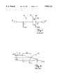
- FIG. 3 is a schematic diagram of a single ended bit line sense amplifier 50 according to the present invention.
- Sense amplifier 50 includes a single ended memory bit line input V I , a capacitor C, complementary enable inputs E and EN, an inverting amplifier 52, a noninverting amplifier 54, a differential amplifier 56 and a sensor output V O '.
- Capacitor C is coupled between bit line input V I and supply terminal GND.
- Inverting amplifier 52 includes a P-channel metal oxide semiconductor field effect transistor (MOSFET) P1 and an N-channel MOSFET N1.
- P-channel MOSFET P1 has a gate coupled to enable input EN, a source coupled to supply terminal VDD and a drain coupled to voltage output node V L .
- MOSFET metal oxide semiconductor field effect transistor
- P-channel MOSFET P1 operates as a selectable current source for voltage output node V L , which is enabled by enable input EN.
- N-channel MOSFET N1 has a gate coupled to bit line input V I , a drain coupled to voltage output node V L and a source coupled to supply terminal GND.
- N-channel MOSFET N1 operates as a pull-down device which pulls voltage output node V L low toward supply terminal GND as a function of the logic state on bit line input V I .
- Noninverting amplifier 54 includes N-channel MOSFET N2 and N-channel MOSFET N3.
- N-channel MOSFET N2 has a gate coupled to bit line input V I , a drain coupled to supply terminal VDD and a source coupled to voltage output node V H .
- N-channel MOSFET N2 operates as a pull-up device which pulls voltage output node V H high toward VDD as a function of the logic state of bit line input V I .
- N-channel transistor N3 has a gate coupled to enable input E, a drain coupled to voltage output node V H and a source coupled to supply terminal GND.
- N-channel MOSFET N3 operates as a selectable current source for voltage output node V H , which is enabled by enable input E.
- Differential amplifier 56 includes amplifier inputs 58 and 60 which are coupled to voltage output nodes V L and V H , respectively. Differential amplifier 56 has an output 62 which is coupled to sensor output V O '.
- FIG. 4 is a graph which illustrates the voltage characteristics of various nodes in sense amplifier 50 over time, as compared to sense amplifier 10 (shown in FIG. 1).
- bit line input V I is initially precharged to a logic high level.
- Enable input E is initially low and enable input EN is initially high.
- P-channel MOSFET P1 and N-channel MOSFET N3 are off and N-channel MOSFETs N1 and N2 are on.
- N-channel MOSFET N1 pulls voltage output node V L low and N-channel MOSFET N2 pulls voltage output node V H high. Therefore, V L ⁇ V H .
- Differential amplifier 56 senses the relative polarity of V L and V H , and drives sensor output V O ' to a logic high level, indicating the logic state of bit line input V I during the precharge state.
- bit line V I is removed and enable inputs E and EN change state.
- P-channel MOSFET P1 and N-channel MOSFET N3 turn on and supply current to voltage output nodes V L and V H , respectively. If bit line input V I stays high, indicating that the data is high, N-channel MOSFETs N1 and N2 stay on and therefore divide the voltages at voltage output nodes V L and V H with MOSFETs P1 and P2.
- the voltage at node V L increases to level 70 as shown in FIG. 4, and the voltage at node V H decreases to level 72. However, the voltages at nodes V L and V H maintain the same relative polarity with V L ⁇ V H .
- the voltages on nodes V L and V H are shifted to analog differential levels for sensing by differential amplifier 56.
- Differential amplifier 56 senses the relative polarity of V L and V H and drives sensor output V O ' high as in the precharged state.
- bit line input V I drops, indicating that the data is low.
- N-channel MOSFETs N1 and N2 turn off. Since P-channel MOSFET P1 and N-channel MOSFET N3 are still on, the voltage on node V L increases and the voltage on node V H decreases.
- the polarity of nodes V L and V H switches such that V L >V H .
- Differential amplifier 56 senses the change in polarity and drives sensor output V O ' low at time t 4 .
- the change in polarity of nodes V L and V H is sensed very quickly since the voltages at nodes V L and V H have been level shifted.
- Differential amplifier 56 does not have to wait for a full logic level change. Rather, differential amplifier 56 has to wait only for a change in polarity of a relatively low differential voltage across nodes V L and V H .
- the output voltage on output V O of sense amplifier 10 shown in FIG. 1 has been inverted and superimposed on FIG. 4 for comparison.
- the output V O drops at a much later time, t 5 , than the output V O ' of the present invention.
- the difference in time, t 5 -t 4 , shown by arrow 64 represents the relative increase in sensing speed between sense amplifier 50 of the invention and sense amplifier 10 shown in FIG. 1.
- sense amplifier 50 does not rely directly on the threshold voltage of P-channel MOSFET P1 to produce the differential voltage at nodes V L and V H when those nodes are at the common-mode sensing range of differential amplifier 56.
- FIG. 5 is a more detailed graph which illustrates a comparison of SPICE simulation results of the sense amplifiers shown in FIGS. 1 and 3 over various operating conditions, where VDD equals 3.13 volts.
- the waveforms generated at the various operating nodes have been superimposed on one another.
- Waveform 80 represents enable input E and waveform 82 represents enable input EN, which become active at approximately 0.75 nanoseconds.
- Waveform 84 represents the voltage on bit line input V I when the voltage remains high after the precharge has been removed.
- Waveform 98 represents the voltage on output V O of sense amplifier 10 shown in FIG. 1, which has been inverted for comparison.
- Arrow 100 represents the decrease in delay on the output of the sense amplifier of the present invention as compared to the output of the sense amplifier shown in FIG. 1 in response to a change in state of the bit line input V I .
- the delay decreased by 1 nanosecond over a cycle time of 5 nanoseconds.
- the sense amplifier of the present invention therefore significantly speeds the sense timing for single ended sense applications.
- the sense amplifier of the present invention does not rely directly on a P-channel threshold voltage to produce a differential voltage, in a common mode sensing range.
- the sense amplifier of the present invention therefore provides fast, single ended sense capability with robust operation over all process, voltage and temperature variations. Since there is no direct dependence on a P-channel threshold voltage, the sense amplifier of the present invention is particularly useful for low voltage applications such as applications with supply voltages of less than two volts.
- enable inputs E and EN can include a pair of complementary enable signals or can include a single enable signal, depending upon the particular circuit configuration of the current sources.
- Each current sources can have a variety of configurations, such as a resistor, a P-channel MOSFET, an N-channel MOSFET or a network of P-channel or N-channel MOSFETs.
- the pull-down and pull-up devices within inverting amplifier 52 and noninverting amplifier 54 can also have a variety of configurations.
- a variety of differential amplifiers can be used with the present invention.
- the sense amplifier of the present invention can be implemented with various technologies other than MOS technology.
- the voltage supply terminals can be relatively positive or relatively negative, depending upon the particular convention adopted and the technology used.
- the terms "pull-up” and “pull-down” used in the specification and the claims are arbitrary terms and can refer to either a logic high level or a logic low level, depending upon the relative levels of the voltage supply terminals.
- the term “coupled” can include various types of connections or couplings and can include a direction connection or a connection through one or more intermediate components.
Landscapes
- Static Random-Access Memory (AREA)
- Dram (AREA)
Abstract
Description
Claims (11)
Priority Applications (2)
| Application Number | Priority Date | Filing Date | Title |
|---|---|---|---|
| US08/698,343 US5825212A (en) | 1996-08-15 | 1996-08-15 | High speed single ended bit line sense amplifier |
| JP9219524A JPH1069786A (en) | 1996-08-15 | 1997-08-14 | Single ended bit line sensor and detecting method for logical state of input of single ended bit line |
Applications Claiming Priority (1)
| Application Number | Priority Date | Filing Date | Title |
|---|---|---|---|
| US08/698,343 US5825212A (en) | 1996-08-15 | 1996-08-15 | High speed single ended bit line sense amplifier |
Publications (1)
| Publication Number | Publication Date |
|---|---|
| US5825212A true US5825212A (en) | 1998-10-20 |
Family
ID=24804856
Family Applications (1)
| Application Number | Title | Priority Date | Filing Date |
|---|---|---|---|
| US08/698,343 Expired - Lifetime US5825212A (en) | 1996-08-15 | 1996-08-15 | High speed single ended bit line sense amplifier |
Country Status (2)
| Country | Link |
|---|---|
| US (1) | US5825212A (en) |
| JP (1) | JPH1069786A (en) |
Cited By (2)
| Publication number | Priority date | Publication date | Assignee | Title |
|---|---|---|---|---|
| US20100039173A1 (en) * | 2008-08-13 | 2010-02-18 | Industrial Technology Research Institute | Single-ended sense amplifier using dynamic reference voltage and operation method thereof |
| US8254195B2 (en) | 2010-06-01 | 2012-08-28 | Qualcomm Incorporated | High-speed sensing for resistive memories |
Citations (4)
| Publication number | Priority date | Publication date | Assignee | Title |
|---|---|---|---|---|
| US4973864A (en) * | 1988-07-13 | 1990-11-27 | Kabushiki Kaisha Toshiba | Sense circuit for use in semiconductor memory |
| US5012450A (en) * | 1987-08-18 | 1991-04-30 | Siemens Aktiengesellschaft | Read amplifier for static memories in CMOS technology |
| US5293088A (en) * | 1989-05-16 | 1994-03-08 | Fujitsu Limited | Sense amplifier circuit |
| US5644258A (en) * | 1996-01-04 | 1997-07-01 | Winbond Electronics Corp. | Driver circuit, with low idle power consumption, for an attachment unit interface |
-
1996
- 1996-08-15 US US08/698,343 patent/US5825212A/en not_active Expired - Lifetime
-
1997
- 1997-08-14 JP JP9219524A patent/JPH1069786A/en active Pending
Patent Citations (4)
| Publication number | Priority date | Publication date | Assignee | Title |
|---|---|---|---|---|
| US5012450A (en) * | 1987-08-18 | 1991-04-30 | Siemens Aktiengesellschaft | Read amplifier for static memories in CMOS technology |
| US4973864A (en) * | 1988-07-13 | 1990-11-27 | Kabushiki Kaisha Toshiba | Sense circuit for use in semiconductor memory |
| US5293088A (en) * | 1989-05-16 | 1994-03-08 | Fujitsu Limited | Sense amplifier circuit |
| US5644258A (en) * | 1996-01-04 | 1997-07-01 | Winbond Electronics Corp. | Driver circuit, with low idle power consumption, for an attachment unit interface |
Non-Patent Citations (2)
| Title |
|---|
| Sedra et al., "Microelectronic Circuits," CBS College Publishing, 2nd edition, pp. 362-363, 1987. |
| Sedra et al., Microelectronic Circuits, CBS College Publishing, 2nd edition, pp. 362 363, 1987. * |
Cited By (3)
| Publication number | Priority date | Publication date | Assignee | Title |
|---|---|---|---|---|
| US20100039173A1 (en) * | 2008-08-13 | 2010-02-18 | Industrial Technology Research Institute | Single-ended sense amplifier using dynamic reference voltage and operation method thereof |
| US7768321B2 (en) | 2008-08-13 | 2010-08-03 | Industrial Technology Research Institute | Single-ended sense amplifier using dynamic reference voltage and operation method thereof |
| US8254195B2 (en) | 2010-06-01 | 2012-08-28 | Qualcomm Incorporated | High-speed sensing for resistive memories |
Also Published As
| Publication number | Publication date |
|---|---|
| JPH1069786A (en) | 1998-03-10 |
Similar Documents
| Publication | Publication Date | Title |
|---|---|---|
| US6717448B2 (en) | Data output method and data output circuit for applying reduced precharge level | |
| US4677321A (en) | TTL compatible input buffer | |
| US7583110B2 (en) | High-speed, low-power input buffer for integrated circuit devices | |
| JPH11308088A (en) | Output buffer circuit | |
| US4617477A (en) | Symmetrical output complementary buffer | |
| JPH0312894A (en) | Sense amplifier driver in memory cell | |
| JP2812162B2 (en) | Current comparator | |
| KR100307637B1 (en) | Input buffer circuit including boosting capacitor | |
| EP0642226A2 (en) | Translator circuits with symmetrical switching delays | |
| US6777985B2 (en) | Input/output buffer having reduced skew and methods of operation | |
| JP2968826B2 (en) | Current mirror type amplifier circuit and driving method thereof | |
| US5825212A (en) | High speed single ended bit line sense amplifier | |
| US5646905A (en) | Self-clocking sense amplifier optimized for input signals close to VDD | |
| US6819143B1 (en) | Input buffer circuit having equal duty cycle | |
| US6140844A (en) | Amplifier | |
| US5734271A (en) | Wideband power driver with separate setting delays of leading and trailing edges | |
| JP3878419B2 (en) | Semiconductor integrated circuit | |
| KR960002334B1 (en) | Input buffer of semiconductor memory device | |
| US20180323775A1 (en) | Resistor-Capacitor (RC) Delay Circuit With A Precharge Mode | |
| EP0136486A2 (en) | Latching output buffer | |
| KR0132369B1 (en) | Data input buffer for semiconductor integrated device and buffering method thereof | |
| KR100245559B1 (en) | Data output buffer circuit | |
| JP3233069B2 (en) | High withstand voltage level detection circuit | |
| JP2919130B2 (en) | Test signal generation circuit | |
| KR100293826B1 (en) | Output Buffer Circuit_ |
Legal Events
| Date | Code | Title | Description |
|---|---|---|---|
| AS | Assignment |
Owner name: LSI LOGIC CORPORATION, CALIFORNIA Free format text: ASSIGNMENT OF ASSIGNORS INTEREST;ASSIGNOR:PRIEBE, GORDON W.;REEL/FRAME:008160/0576 Effective date: 19960814 |
|
| STCF | Information on status: patent grant |
Free format text: PATENTED CASE |
|
| FPAY | Fee payment |
Year of fee payment: 4 |
|
| FPAY | Fee payment |
Year of fee payment: 8 |
|
| FEPP | Fee payment procedure |
Free format text: PAYER NUMBER DE-ASSIGNED (ORIGINAL EVENT CODE: RMPN); ENTITY STATUS OF PATENT OWNER: LARGE ENTITY Free format text: PAYOR NUMBER ASSIGNED (ORIGINAL EVENT CODE: ASPN); ENTITY STATUS OF PATENT OWNER: LARGE ENTITY |
|
| FPAY | Fee payment |
Year of fee payment: 12 |
|
| AS | Assignment |
Owner name: DEUTSCHE BANK AG NEW YORK BRANCH, AS COLLATERAL AGENT, NEW YORK Free format text: PATENT SECURITY AGREEMENT;ASSIGNORS:LSI CORPORATION;AGERE SYSTEMS LLC;REEL/FRAME:032856/0031 Effective date: 20140506 Owner name: DEUTSCHE BANK AG NEW YORK BRANCH, AS COLLATERAL AG Free format text: PATENT SECURITY AGREEMENT;ASSIGNORS:LSI CORPORATION;AGERE SYSTEMS LLC;REEL/FRAME:032856/0031 Effective date: 20140506 |
|
| AS | Assignment |
Owner name: LSI CORPORATION, CALIFORNIA Free format text: CHANGE OF NAME;ASSIGNOR:LSI LOGIC CORPORATION;REEL/FRAME:033102/0270 Effective date: 20070406 |
|
| AS | Assignment |
Owner name: AVAGO TECHNOLOGIES GENERAL IP (SINGAPORE) PTE. LTD Free format text: ASSIGNMENT OF ASSIGNORS INTEREST;ASSIGNOR:LSI CORPORATION;REEL/FRAME:035390/0388 Effective date: 20140814 |
|
| AS | Assignment |
Owner name: LSI CORPORATION, CALIFORNIA Free format text: TERMINATION AND RELEASE OF SECURITY INTEREST IN PATENT RIGHTS (RELEASES RF 032856-0031);ASSIGNOR:DEUTSCHE BANK AG NEW YORK BRANCH, AS COLLATERAL AGENT;REEL/FRAME:037684/0039 Effective date: 20160201 Owner name: AGERE SYSTEMS LLC, PENNSYLVANIA Free format text: TERMINATION AND RELEASE OF SECURITY INTEREST IN PATENT RIGHTS (RELEASES RF 032856-0031);ASSIGNOR:DEUTSCHE BANK AG NEW YORK BRANCH, AS COLLATERAL AGENT;REEL/FRAME:037684/0039 Effective date: 20160201 |
|
| AS | Assignment |
Owner name: BANK OF AMERICA, N.A., AS COLLATERAL AGENT, NORTH CAROLINA Free format text: PATENT SECURITY AGREEMENT;ASSIGNOR:AVAGO TECHNOLOGIES GENERAL IP (SINGAPORE) PTE. LTD.;REEL/FRAME:037808/0001 Effective date: 20160201 Owner name: BANK OF AMERICA, N.A., AS COLLATERAL AGENT, NORTH Free format text: PATENT SECURITY AGREEMENT;ASSIGNOR:AVAGO TECHNOLOGIES GENERAL IP (SINGAPORE) PTE. LTD.;REEL/FRAME:037808/0001 Effective date: 20160201 |
|
| AS | Assignment |
Owner name: AVAGO TECHNOLOGIES GENERAL IP (SINGAPORE) PTE. LTD., SINGAPORE Free format text: TERMINATION AND RELEASE OF SECURITY INTEREST IN PATENTS;ASSIGNOR:BANK OF AMERICA, N.A., AS COLLATERAL AGENT;REEL/FRAME:041710/0001 Effective date: 20170119 Owner name: AVAGO TECHNOLOGIES GENERAL IP (SINGAPORE) PTE. LTD Free format text: TERMINATION AND RELEASE OF SECURITY INTEREST IN PATENTS;ASSIGNOR:BANK OF AMERICA, N.A., AS COLLATERAL AGENT;REEL/FRAME:041710/0001 Effective date: 20170119 |