US5729185A - Acoustic wave filter package lid attachment apparatus and method utilizing a novolac epoxy based seal - Google Patents
Acoustic wave filter package lid attachment apparatus and method utilizing a novolac epoxy based seal Download PDFInfo
- Publication number
- US5729185A US5729185A US08/639,673 US63967396A US5729185A US 5729185 A US5729185 A US 5729185A US 63967396 A US63967396 A US 63967396A US 5729185 A US5729185 A US 5729185A
- Authority
- US
- United States
- Prior art keywords
- wafer
- acoustic wave
- lithium
- seal ring
- wave filter
- Prior art date
- Legal status (The legal status is an assumption and is not a legal conclusion. Google has not performed a legal analysis and makes no representation as to the accuracy of the status listed.)
- Expired - Fee Related
Links
Images

Classifications
-
- H—ELECTRICITY
- H03—ELECTRONIC CIRCUITRY
- H03H—IMPEDANCE NETWORKS, e.g. RESONANT CIRCUITS; RESONATORS
- H03H9/00—Networks comprising electromechanical or electro-acoustic elements; Electromechanical resonators
- H03H9/02—Details
- H03H9/05—Holders or supports
- H03H9/10—Mounting in enclosures
- H03H9/1064—Mounting in enclosures for surface acoustic wave [SAW] devices
- H03H9/1092—Mounting in enclosures for surface acoustic wave [SAW] devices the enclosure being defined by a cover cap mounted on an element forming part of the surface acoustic wave [SAW] device on the side of the IDT's
-
- Y—GENERAL TAGGING OF NEW TECHNOLOGICAL DEVELOPMENTS; GENERAL TAGGING OF CROSS-SECTIONAL TECHNOLOGIES SPANNING OVER SEVERAL SECTIONS OF THE IPC; TECHNICAL SUBJECTS COVERED BY FORMER USPC CROSS-REFERENCE ART COLLECTIONS [XRACs] AND DIGESTS
- Y10—TECHNICAL SUBJECTS COVERED BY FORMER USPC
- Y10T—TECHNICAL SUBJECTS COVERED BY FORMER US CLASSIFICATION
- Y10T29/00—Metal working
- Y10T29/42—Piezoelectric device making
Definitions
- This invention relates in general to the field of frequency selection component packages, in particular to surface acoustic wave frequency selection component packages and more particularly to a simplified technique for lid attachment for acoustic wave frequency selection component packages.
- Acoustic wave devices are becoming particularly important in the construction of electronic signal processing equipment, such as radios, paging devices, and other high frequency electronic apparatus, because they can be readily constructed on planar surfaces using integrated circuit fabrication techniques, are robust and compact, require no initial or periodic adjustment and consume no static power.
- SAW resonators and other types of acoustic wave frequency selection components are extremely desirable for high frequency filtering applications.
- a second problem that hermetically sealed packages engender is that the finished, packaged device is typically much larger than the SAW device die.
- a reduction in size and/or weight of the completed and packaged frequency selection component provides significant advantages in the applications for which these devices are designed, e.g., portable telephones, paging apparatus and the like.
- hermetic packages typically include a higher labor and material content than, e.g., transfer molded packages. This, in turn, is reflected in the total labor content of the completed communications apparatus in which these devices are used.
- FIG. 1 is a simplified plan view of a wafer of acoustic wave filter dice
- FIG. 2 is a simplified plan view of an acoustic wave filter die in accordance with the present invention.
- FIG. 3 is a side view, in section, taken along section lines III--III of FIG. 2, showing the acoustic wave filter die with an attached lid in accordance with the present invention.
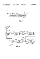
- FIG. 4 is a block diagram of a portion of a radio frequency apparatus including acoustic wave filters in accordance with the present invention.
- FIG. 1 is a simplified plan view of wafer 100 including acoustic wave filter dice 102.
- wafer 100 is diced by a high speed saw along scribe lines 103, 103' to separate individual die 102 for packaging.
- Substrate or wafer 100 typically comprises crystalline quartz, lithium niobate (LiNbO 3 ), lithium tantalate (LiTaO 3 ), lithium tetraborate (Li 2 B 4 O 7 ) or zinc oxide films deposited on suitable substrata and includes a polished surface upon which device patterns are formed by photolithographic techniques similar to those employed in the manufacture of integrated circuits or other microelectronic components.
- FIG. 2 is a simplified plan view of acoustic wave filter die 102 in accordance with the present invention.
- Die 102 is illustrated as including two surface acoustic wave transducers 18, 18', but it will be appreciated that more or fewer transducers 18, 18' may be included for specific performance reasons.
- Each transducer 18, 18' includes bond pads 20 and interdigitated electrodes 21.
- the region including electrodes 21 and areas between electrodes 21 is referred to herein as the "active region" and is enclosed within inner border 26 of seal ring 25.
- seal ring 25 may be conveniently realized by dispensing and photolithographically shaping photosensitive epoxy on the surface of wafer 100 prior to dicing.
- Photosensitive epoxy may be realized as SU-8-75 novolac epoxy available from Shell Chemical Co. of Houston Tex. combined with methyl ethyl ketone (MEK) (or other suitable casting solvent) in proportions such as 75:25 by weight. More or less casting solvent may be employed as desired to achieve a particular film thickness.
- MEK methyl ethyl ketone
- An onium salt is then added in an amount ranging from 1 to 10 percent by weight to achieve a desired range of sensitivity to ultraviolet light exposure.
- the mixture previously given might then be mixed to include 90:10 by weight with Cyracure UVI 6074 available from Union Carbide of Danbury Conn.
- This mixture may be spun on at a speed of 600 rpm to realize a film of thickness of about 20 micrometers.
- Various thicknesses may be useful; generally thicknesses in a range of one to forty micrometers are of utility with respect to the instant invention.
- Other onium salts are usefully employed for providing the desired photosensitivity. Examples include Cyracure-6076 and General Electric UVE-1014 or -1016.
- the layer is cured via a bake at 95° C. for five minutes.
- epoxy may be removed from other areas of die 102 by rinsing in propylene glycol monoethyl acetate for a period of five minutes.
- a post-exposure bake (laying flat) at 100°-120° C. for ten minutes is then carried out.
- Seal ring 25 has several requirements; (i) it must completely surround and enclose the active area of die 102, (ii) it must not extend into the active area of die 102 to any significant extent, (iii) it must not provide contamination of the active area of die 102, for example, by outgassing, (iv) it must allow pads 20 to extend from within the active area of die 102 to an area outside seal ring 25 and (v) it, together with an adhesive layer (not illustrated) disposed between seal ring 25 and lid 40 (FIG. 3), must secure lid 40 to die 102 and prevent intrusion of foreign materials during overmolding and at any other time.
- the latter requirement includes maintaining integrity of seal ring 25 under conditions of 160°-190° C.
- seal ring 25 together with lid 40 is that (vi) they must separate the lower surface of lid 40 from the active area of the die to a suitable extent (at least a few micrometers).
- lid 40 allows lid 40 to be attached to die 102 while still in wafer form. This is effected by, for example, placing a second wafer (not illustrated), preferably but not necessarily of the same material as substrate 102 and desirably having similar crystallographic orientation, atop wafer 100 after deposition and patterning of seal ring 25 and application of a sealing material (not illustrated) to a second wafer that will become lid 40, applying pressure and curing the layer of sealing material disposed on one side of the second wafer to effect a seal.
- a second wafer preferably but not necessarily of the same material as substrate 102 and desirably having similar crystallographic orientation
- the sealing material may comprise a suitable thermoplastic thinned with casting solvent and spun onto the second wafer, a UV curable epoxy such as described in connection with seal ring 25 or other microelectronic grade sealing material or adhesive consistent with the properties listed supra for seal ring 25.
- lid 40/second wafer may comprise metals (e.g., Cu), ceramic or glass materials having suitably chosen thermal expansion characteristics.
- Advantages of using the same material for both the first 100 and second wafers include the fact that most SAW substrates comprise materials transparent to visible light, allowing ready alignment of both first 100 and second wafers to each other and together to the saw for dicing. Transparency of lid 40 to ultraviolet radiation also permits use of UV curable seal epoxy disposed on the bottom of lid 40 as the agent for sealing lid 40 to seal ring 25. Another advantage is that some SAW substrata have anisotropic thermal expansion properties. Use of a lid structure 40 that matches the thermal properties of die 102 reduces thermally induced stresses on seal ring 25.
- the second wafer includes recesses (dashed line 41, FIG. 3) disposed to coincide with the active area of SAW die 102. This prevents the lid from contacting the active area.
- seal ring 25 is made to be tall enough to provide adequate clearance over the active area. Bond pads 20 extend beyond seal ring 25, allowing electrical interconnection of transducers 18, 18' to external electrical apparatus.
- the sandwich of wafer 100 and the second wafer may then be diced, first slicing the second wafer with a blade having a wide kerf (e.g., ca. 1 mm or 40 mils) along scribe lines 103, 103' and then slicing wafer 100 with a blade having a narrower kerf (e.g., 125-150 micrometers or 5-6 mils).
- a wide kerf e.g., ca. 1 mm or 40 mils
- a narrower kerf e.g., 125-150 micrometers or 5-6 mils.
- FIG. 3 is a side view, in section, taken along section lines III--III of FIG. 2, showing acoustic wave filter die 102 with attached lid 40 in accordance with the present invention.
- Lid 40 is shown as being spaced apart from the surface of die 102 by seal ring 25 and/or via cavity 41 within the lower surface of lid 40.
- Bond pads 20 extend beyond the edges of lid 40 to allow interconnection of transducers 18, 18' to external apparatus.
- the assembled device may be encapsulated by conventional transfer molding to provide a packaged SAW device that is compact, lightweight and robust.
- FIG. 4 is a block diagram of portion 1200 of a radio or other communications apparatus including one or more acoustic wave filters in accordance with the present invention.
- Apparatus 1200 includes antenna 1201 and antenna lead 1204, by way of example, used to receive and/or transmit signals.
- antenna 1201 and antenna lead 1204 could be replaced by a fiber-optic link or a cable or other signal transmissive media.
- Diplexer 1209 is coupled to antenna 1201 and antenna lead 1204 and to a transmitter portion (not shown). Diplexer 1209 couples received signals to filter 1215 via lead 1212. Filter 1215 is coupled to amplifier 1227 via lead 1226.
- the output of amplifier 1227 is coupled to filter 1239 via lead 1233.
- Filter 1239 couples its output signal to mixer 1265 where the signal coupled by lead 1242 is combined with another signal from local oscillator 1244 coupled via filter 1255 and leads 1249 and 1259.
- the signal which is output from mixer 1265 via lead 1271 is then passed through filter 1277 to provide an intermediate frequency or IF output signal via lead 1280.
- Diplexer 1209, filter 1215, filter 1239, filter 1255 and/or filter 1277 may comprise acoustic wave filters according to the present invention.
- a SAW device package has been described which overcomes specific problems and accomplishes certain advantages relative to prior art methods and mechanisms.
- the improvements over known technology are significant.
- the expense, complexities, and higher labor content of prior art approaches are avoided.
- a compact yet robust device package is provided that allows relaxed package specifications and reduced size and weight of the completed and packaged filter.
Landscapes
- Physics & Mathematics (AREA)
- Acoustics & Sound (AREA)
- Surface Acoustic Wave Elements And Circuit Networks Thereof (AREA)
Priority Applications (3)
| Application Number | Priority Date | Filing Date | Title |
|---|---|---|---|
| US08/639,673 US5729185A (en) | 1996-04-29 | 1996-04-29 | Acoustic wave filter package lid attachment apparatus and method utilizing a novolac epoxy based seal |
| EP97106536A EP0805552A3 (de) | 1996-04-29 | 1997-04-21 | Packung für akustisches Wellenfilter und Herstellungsverfahren |
| JP9117551A JPH1075140A (ja) | 1996-04-29 | 1997-04-21 | 音響波フィルタ・パッケージおよび方法 |
Applications Claiming Priority (1)
| Application Number | Priority Date | Filing Date | Title |
|---|---|---|---|
| US08/639,673 US5729185A (en) | 1996-04-29 | 1996-04-29 | Acoustic wave filter package lid attachment apparatus and method utilizing a novolac epoxy based seal |
Publications (1)
| Publication Number | Publication Date |
|---|---|
| US5729185A true US5729185A (en) | 1998-03-17 |
Family
ID=24565097
Family Applications (1)
| Application Number | Title | Priority Date | Filing Date |
|---|---|---|---|
| US08/639,673 Expired - Fee Related US5729185A (en) | 1996-04-29 | 1996-04-29 | Acoustic wave filter package lid attachment apparatus and method utilizing a novolac epoxy based seal |
Country Status (3)
| Country | Link |
|---|---|
| US (1) | US5729185A (de) |
| EP (1) | EP0805552A3 (de) |
| JP (1) | JPH1075140A (de) |
Cited By (10)
| Publication number | Priority date | Publication date | Assignee | Title |
|---|---|---|---|---|
| US6182342B1 (en) | 1999-04-02 | 2001-02-06 | Andersen Laboratories, Inc. | Method of encapsulating a saw device |
| US20030012884A1 (en) * | 2000-02-14 | 2003-01-16 | Wolfgang Pahl | Encapsulation for an electrical component and method for producing the same |
| US20050106785A1 (en) * | 2002-04-12 | 2005-05-19 | Frank Daeche | Method for manufacturing a housing for a chip with a micromechanical structure |
| US20050269902A1 (en) * | 2004-06-04 | 2005-12-08 | Jack Thiesen | Reducing coupling of RF interrogated SAWs to external bodies |
| US20060055286A1 (en) * | 2004-09-14 | 2006-03-16 | Honeywell International, Inc. | Surface acoustic wave die methods and systems |
| US20060255454A1 (en) * | 2005-05-10 | 2006-11-16 | Kirby Sand | Wafer bonding method |
| US20070126072A1 (en) * | 2005-12-07 | 2007-06-07 | Honeywell International Inc. | Surface acoustic wave pressure sensors |
| US20090189488A1 (en) * | 2008-01-29 | 2009-07-30 | Hyde Park Electronics Llc | Ultrasonic transducer for a proximity sensor |
| US20100107400A1 (en) * | 2006-05-17 | 2010-05-06 | Avago Technologies Wireless Ip (Singapore) Pte.Ltd | Method of manufacturing an acoustic mirror |
| US20100309018A1 (en) * | 2008-01-29 | 2010-12-09 | Schneider Electric USA, Inc. | Ultrasonic transducer for a proximity sensor |
Families Citing this family (3)
| Publication number | Priority date | Publication date | Assignee | Title |
|---|---|---|---|---|
| JP3123477B2 (ja) * | 1997-08-08 | 2001-01-09 | 日本電気株式会社 | 表面弾性波素子の実装構造および実装方法 |
| JP4813692B2 (ja) * | 2001-06-15 | 2011-11-09 | セイコーインスツル株式会社 | 気密封止icパッケージの製造方法 |
| DE10206919A1 (de) * | 2002-02-19 | 2003-08-28 | Infineon Technologies Ag | Verfahren zur Erzeugung einer Abdeckung, Verfahren zum Herstellen eines gehäusten Bauelements |
Citations (29)
| Publication number | Priority date | Publication date | Assignee | Title |
|---|---|---|---|---|
| GB1389610A (en) * | 1972-10-11 | 1975-04-03 | Marconi Co Ltd | Surfacewave devices |
| US4047129A (en) * | 1975-03-13 | 1977-09-06 | Murata Manufacturing Co., Ltd. | Elastic surface wave filter |
| US4213104A (en) * | 1978-09-25 | 1980-07-15 | United Technologies Corporation | Vacuum encapsulation for surface acoustic wave (SAW) devices |
| US4282498A (en) * | 1978-09-22 | 1981-08-04 | Matsushima Kogyo Kabushiki Kaisha | Circuit package |
| US4291285A (en) * | 1979-02-22 | 1981-09-22 | Murata Manufacturing Co., Ltd. | Surface acoustic wave device and method of manufacturing |
| US4295102A (en) * | 1979-09-28 | 1981-10-13 | Texas Instruments Incorporated | Surface acoustic wave sensor sensing circuits |
| US4296347A (en) * | 1979-09-28 | 1981-10-20 | Texas Instruments Incorporated | Surface acoustic wave sensor |
| US4306456A (en) * | 1979-03-30 | 1981-12-22 | Thomson-Csf | Elastic wave accelerometer |
| US4365219A (en) * | 1981-02-27 | 1982-12-21 | General Electric Company | In-line surface acoustic wave filter assembly module and method of making same |
| JPS5977715A (ja) * | 1982-10-26 | 1984-05-04 | Murata Mfg Co Ltd | チツプ状圧電振動部品 |
| US4450374A (en) * | 1982-05-27 | 1984-05-22 | Motorola Inc. | Oxygen-plasma passivated and low scatter acoustic wave devices |
| US4480148A (en) * | 1981-05-13 | 1984-10-30 | Plessey Overseas Limited | Electrical device package |
| US4571794A (en) * | 1982-07-22 | 1986-02-25 | Murata Manufacturing Co., Ltd. | Method of accommodating electronic component in casing |
| US4628146A (en) * | 1984-03-23 | 1986-12-09 | Siemens Aktiengesellschaft | Casing for electrical components, component assemblies or integrated circuits |
| US4699682A (en) * | 1985-10-23 | 1987-10-13 | Clarion Co., Ltd. | Surface acoustic wave device sealing method |
| US4737742A (en) * | 1986-01-28 | 1988-04-12 | Alps Electric Co., Ltd. | Unit carrying surface acoustic wave devices |
| JPH0349310A (ja) * | 1989-07-17 | 1991-03-04 | Murata Mfg Co Ltd | 弾性表面波デバイス |
| US5043221A (en) * | 1985-12-19 | 1991-08-27 | Union Carbide Chemicals And Plastics Technology Corporation | Conformal coatings cured with actinic radiation |
| US5059848A (en) * | 1990-08-20 | 1991-10-22 | The United States Of America As Represented By The Secretary Of The Army | Low-cost saw packaging technique |
| US5162822A (en) * | 1988-10-31 | 1992-11-10 | Hitachi, Ltd. | Saw filter chip mounted on a substrate with shielded conductors on opposite surfaces |
| JPH0590882A (ja) * | 1991-09-28 | 1993-04-09 | Murata Mfg Co Ltd | 弾性表面波装置及びその製造方法 |
| US5237235A (en) * | 1991-09-30 | 1993-08-17 | Motorola, Inc. | Surface acoustic wave device package |
| JPH06132759A (ja) * | 1992-10-21 | 1994-05-13 | Toshiba Corp | 電子部品装置の製造方法 |
| US5337026A (en) * | 1984-09-13 | 1994-08-09 | Raytheon Company | SAW device and method of manufacturing |
| US5345201A (en) * | 1988-06-29 | 1994-09-06 | Raytheon Company | Saw device and method of manufacture |
| US5361967A (en) * | 1993-11-10 | 1994-11-08 | Motorola, Inc. | Monolithic circuit fabrication method |
| US5410789A (en) * | 1992-11-13 | 1995-05-02 | Murata Manufacturing Co., Ltd. | Method of manufacturing piezoelectric-resonator having vibrating spaces formed therein |
| US5414917A (en) * | 1992-10-19 | 1995-05-16 | Murata Manufacturing Co., Ltd. | Method of manufacturing piezoelectric resonator chips |
| WO1996039632A1 (en) * | 1995-06-06 | 1996-12-12 | Analog Devices, Inc. | Package for sealing an integrated circuit die |
Family Cites Families (2)
| Publication number | Priority date | Publication date | Assignee | Title |
|---|---|---|---|---|
| JP3222220B2 (ja) * | 1992-10-19 | 2001-10-22 | 株式会社村田製作所 | チップ型圧電共振子の製造方法 |
| JPH0823259A (ja) * | 1994-07-08 | 1996-01-23 | Kokusai Electric Co Ltd | 弾性表面波装置とその製造方法 |
-
1996
- 1996-04-29 US US08/639,673 patent/US5729185A/en not_active Expired - Fee Related
-
1997
- 1997-04-21 JP JP9117551A patent/JPH1075140A/ja active Pending
- 1997-04-21 EP EP97106536A patent/EP0805552A3/de not_active Withdrawn
Patent Citations (29)
| Publication number | Priority date | Publication date | Assignee | Title |
|---|---|---|---|---|
| GB1389610A (en) * | 1972-10-11 | 1975-04-03 | Marconi Co Ltd | Surfacewave devices |
| US4047129A (en) * | 1975-03-13 | 1977-09-06 | Murata Manufacturing Co., Ltd. | Elastic surface wave filter |
| US4282498A (en) * | 1978-09-22 | 1981-08-04 | Matsushima Kogyo Kabushiki Kaisha | Circuit package |
| US4213104A (en) * | 1978-09-25 | 1980-07-15 | United Technologies Corporation | Vacuum encapsulation for surface acoustic wave (SAW) devices |
| US4291285A (en) * | 1979-02-22 | 1981-09-22 | Murata Manufacturing Co., Ltd. | Surface acoustic wave device and method of manufacturing |
| US4306456A (en) * | 1979-03-30 | 1981-12-22 | Thomson-Csf | Elastic wave accelerometer |
| US4296347A (en) * | 1979-09-28 | 1981-10-20 | Texas Instruments Incorporated | Surface acoustic wave sensor |
| US4295102A (en) * | 1979-09-28 | 1981-10-13 | Texas Instruments Incorporated | Surface acoustic wave sensor sensing circuits |
| US4365219A (en) * | 1981-02-27 | 1982-12-21 | General Electric Company | In-line surface acoustic wave filter assembly module and method of making same |
| US4480148A (en) * | 1981-05-13 | 1984-10-30 | Plessey Overseas Limited | Electrical device package |
| US4450374A (en) * | 1982-05-27 | 1984-05-22 | Motorola Inc. | Oxygen-plasma passivated and low scatter acoustic wave devices |
| US4571794A (en) * | 1982-07-22 | 1986-02-25 | Murata Manufacturing Co., Ltd. | Method of accommodating electronic component in casing |
| JPS5977715A (ja) * | 1982-10-26 | 1984-05-04 | Murata Mfg Co Ltd | チツプ状圧電振動部品 |
| US4628146A (en) * | 1984-03-23 | 1986-12-09 | Siemens Aktiengesellschaft | Casing for electrical components, component assemblies or integrated circuits |
| US5337026A (en) * | 1984-09-13 | 1994-08-09 | Raytheon Company | SAW device and method of manufacturing |
| US4699682A (en) * | 1985-10-23 | 1987-10-13 | Clarion Co., Ltd. | Surface acoustic wave device sealing method |
| US5043221A (en) * | 1985-12-19 | 1991-08-27 | Union Carbide Chemicals And Plastics Technology Corporation | Conformal coatings cured with actinic radiation |
| US4737742A (en) * | 1986-01-28 | 1988-04-12 | Alps Electric Co., Ltd. | Unit carrying surface acoustic wave devices |
| US5345201A (en) * | 1988-06-29 | 1994-09-06 | Raytheon Company | Saw device and method of manufacture |
| US5162822A (en) * | 1988-10-31 | 1992-11-10 | Hitachi, Ltd. | Saw filter chip mounted on a substrate with shielded conductors on opposite surfaces |
| JPH0349310A (ja) * | 1989-07-17 | 1991-03-04 | Murata Mfg Co Ltd | 弾性表面波デバイス |
| US5059848A (en) * | 1990-08-20 | 1991-10-22 | The United States Of America As Represented By The Secretary Of The Army | Low-cost saw packaging technique |
| JPH0590882A (ja) * | 1991-09-28 | 1993-04-09 | Murata Mfg Co Ltd | 弾性表面波装置及びその製造方法 |
| US5237235A (en) * | 1991-09-30 | 1993-08-17 | Motorola, Inc. | Surface acoustic wave device package |
| US5414917A (en) * | 1992-10-19 | 1995-05-16 | Murata Manufacturing Co., Ltd. | Method of manufacturing piezoelectric resonator chips |
| JPH06132759A (ja) * | 1992-10-21 | 1994-05-13 | Toshiba Corp | 電子部品装置の製造方法 |
| US5410789A (en) * | 1992-11-13 | 1995-05-02 | Murata Manufacturing Co., Ltd. | Method of manufacturing piezoelectric-resonator having vibrating spaces formed therein |
| US5361967A (en) * | 1993-11-10 | 1994-11-08 | Motorola, Inc. | Monolithic circuit fabrication method |
| WO1996039632A1 (en) * | 1995-06-06 | 1996-12-12 | Analog Devices, Inc. | Package for sealing an integrated circuit die |
Cited By (21)
| Publication number | Priority date | Publication date | Assignee | Title |
|---|---|---|---|---|
| US6182342B1 (en) | 1999-04-02 | 2001-02-06 | Andersen Laboratories, Inc. | Method of encapsulating a saw device |
| US20030012884A1 (en) * | 2000-02-14 | 2003-01-16 | Wolfgang Pahl | Encapsulation for an electrical component and method for producing the same |
| US6984421B2 (en) * | 2000-02-14 | 2006-01-10 | Epcos Ag | Encapsulation for an electrical component and method for producing the same |
| US7011986B2 (en) | 2002-04-12 | 2006-03-14 | Infineon Technologies Ag | Method for manufacturing a housing for a chip with a micromechanical structure |
| US20050106785A1 (en) * | 2002-04-12 | 2005-05-19 | Frank Daeche | Method for manufacturing a housing for a chip with a micromechanical structure |
| US7224100B2 (en) * | 2004-06-04 | 2007-05-29 | Michelin Recherche Et Technique S.A. | Reducing coupling of RF interrogated SAWs to external bodies |
| US20050269902A1 (en) * | 2004-06-04 | 2005-12-08 | Jack Thiesen | Reducing coupling of RF interrogated SAWs to external bodies |
| US20060055286A1 (en) * | 2004-09-14 | 2006-03-16 | Honeywell International, Inc. | Surface acoustic wave die methods and systems |
| US7165298B2 (en) * | 2004-09-14 | 2007-01-23 | Honeywell International Inc. | Method of making a surface acoustic wave device |
| US20060255454A1 (en) * | 2005-05-10 | 2006-11-16 | Kirby Sand | Wafer bonding method |
| US8390111B2 (en) | 2005-05-10 | 2013-03-05 | Hewlett-Packard Development Company, L.P. | Wafer bonding method |
| US7303976B2 (en) | 2005-05-10 | 2007-12-04 | Hewlett-Packard Development Company, L.P. | Wafer bonding method |
| US20080048313A1 (en) * | 2005-05-10 | 2008-02-28 | Kirby Sand | Wafer Bonding Method |
| US20070126072A1 (en) * | 2005-12-07 | 2007-06-07 | Honeywell International Inc. | Surface acoustic wave pressure sensors |
| US7651879B2 (en) | 2005-12-07 | 2010-01-26 | Honeywell International Inc. | Surface acoustic wave pressure sensors |
| US20100107400A1 (en) * | 2006-05-17 | 2010-05-06 | Avago Technologies Wireless Ip (Singapore) Pte.Ltd | Method of manufacturing an acoustic mirror |
| US8256093B2 (en) | 2006-05-17 | 2012-09-04 | Avago Technologies Wireless Ip (Singapore) Pte. Ltd. | Method of manufacturing an acoustic mirror |
| US7804742B2 (en) | 2008-01-29 | 2010-09-28 | Hyde Park Electronics Llc | Ultrasonic transducer for a proximity sensor |
| US20100309018A1 (en) * | 2008-01-29 | 2010-12-09 | Schneider Electric USA, Inc. | Ultrasonic transducer for a proximity sensor |
| US20090189488A1 (en) * | 2008-01-29 | 2009-07-30 | Hyde Park Electronics Llc | Ultrasonic transducer for a proximity sensor |
| US8456957B2 (en) | 2008-01-29 | 2013-06-04 | Schneider Electric USA, Inc. | Ultrasonic transducer for a proximity sensor |
Also Published As
| Publication number | Publication date |
|---|---|
| EP0805552A2 (de) | 1997-11-05 |
| JPH1075140A (ja) | 1998-03-17 |
| EP0805552A3 (de) | 1998-07-08 |
Similar Documents
| Publication | Publication Date | Title |
|---|---|---|
| US5892417A (en) | Saw device package and method | |
| EP0805552A2 (de) | Packung für akustisches Wellenfilter und Herstellungsverfahren | |
| US7589458B2 (en) | Quartz crystal vibrator, oscillator and electronic apparatus | |
| KR100642932B1 (ko) | 압전 부품 | |
| JP4636882B2 (ja) | 気密に密封された素子、及びこれを製造するための方法 | |
| US5928598A (en) | Method of making a microelectronic device package | |
| US8749122B2 (en) | Piezoelectric vibrator having peripheral notches therein | |
| US8004160B2 (en) | Acoustic wave device with adhesive layer and method of manufacturing the same | |
| US7459094B2 (en) | Method for making a surface acoustic wave device package | |
| EP2267895B1 (de) | Elektronisches Bauelement, Leiterplatte, elektronisches Gerät und Herstellungsverfahren des elektronischen Bauelements | |
| US20110226731A1 (en) | Crystal substrate etching method, piezoelectric vibrating reed, a piezoelectric vibrator, oscillator, electronic device, and radio-controlled timepiece | |
| CN101192815B (zh) | 声波器件及其制造方法 | |
| JP4404450B2 (ja) | 弾性表面波装置及びその製造方法 | |
| US10511285B1 (en) | Anchored polymeric package for acoustic resonator structures | |
| JP2003032061A (ja) | 弾性表面波装置の製造方法 | |
| US20110285245A1 (en) | Anodic wafer bonding method, method of manufacturing packages, method of manufacturing piezoelectric vibrators, oscillator, electronic apparatus, and radio clock | |
| JP2004153412A (ja) | 弾性表面波装置及びその製造方法 | |
| JP2003283295A (ja) | 弾性表面波装置及びその製造方法 | |
| CN118646391A (zh) | 一种体声波谐振器及其制备方法、滤波器 | |
| JP2003264442A (ja) | 弾性表面波装置の製造方法及び多面取りベース基板 | |
| JP2007104458A (ja) | 薄膜圧電共振子デバイスおよびその製造方法 | |
| JP2005217670A (ja) | 弾性表面波装置および通信装置 | |
| US20060113874A1 (en) | Surface acoustic wave device package | |
| JP2004119625A (ja) | 電子部品用蓋体とその製造方法、ならびに圧電デバイスと圧電デバイスを利用した携帯電話装置および圧電デバイスを利用した電子機器 | |
| WO2020126907A1 (en) | Micro-acoustic wafer-level package and method of manufacture |
Legal Events
| Date | Code | Title | Description |
|---|---|---|---|
| AS | Assignment |
Owner name: CTS CORPORATION, INDIANA Free format text: ASSIGNMENT OF ASSIGNORS INTEREST;ASSIGNOR:MOTOROLA, INC., A CORPORATION OF DELAWARE;REEL/FRAME:009808/0378 Effective date: 19990226 |
|
| FEPP | Fee payment procedure |
Free format text: PAYOR NUMBER ASSIGNED (ORIGINAL EVENT CODE: ASPN); ENTITY STATUS OF PATENT OWNER: LARGE ENTITY |
|
| FPAY | Fee payment |
Year of fee payment: 4 |
|
| REMI | Maintenance fee reminder mailed | ||
| LAPS | Lapse for failure to pay maintenance fees | ||
| STCH | Information on status: patent discontinuation |
Free format text: PATENT EXPIRED DUE TO NONPAYMENT OF MAINTENANCE FEES UNDER 37 CFR 1.362 |
|
| FP | Lapsed due to failure to pay maintenance fee |
Effective date: 20060317 |