US5670883A - Integrated circuit interlevel conductor defect characterization test structure and system - Google Patents
Integrated circuit interlevel conductor defect characterization test structure and system Download PDFInfo
- Publication number
- US5670883A US5670883A US08/560,650 US56065095A US5670883A US 5670883 A US5670883 A US 5670883A US 56065095 A US56065095 A US 56065095A US 5670883 A US5670883 A US 5670883A
- Authority
- US
- United States
- Prior art keywords
- conductor
- interlevel
- test
- layer
- integrated circuit
- Prior art date
- Legal status (The legal status is an assumption and is not a legal conclusion. Google has not performed a legal analysis and makes no representation as to the accuracy of the status listed.)
- Expired - Lifetime
Links
Images


Classifications
-
- H—ELECTRICITY
- H01—ELECTRIC ELEMENTS
- H01L—SEMICONDUCTOR DEVICES NOT COVERED BY CLASS H10
- H01L22/00—Testing or measuring during manufacture or treatment; Reliability measurements, i.e. testing of parts without further processing to modify the parts as such; Structural arrangements therefor
- H01L22/30—Structural arrangements specially adapted for testing or measuring during manufacture or treatment, or specially adapted for reliability measurements
- H01L22/34—Circuits for electrically characterising or monitoring manufacturing processes, e. g. whole test die, wafers filled with test structures, on-board-devices incorporated on each die, process control monitors or pad structures thereof, devices in scribe line
-
- G—PHYSICS
- G01—MEASURING; TESTING
- G01R—MEASURING ELECTRIC VARIABLES; MEASURING MAGNETIC VARIABLES
- G01R31/00—Arrangements for testing electric properties; Arrangements for locating electric faults; Arrangements for electrical testing characterised by what is being tested not provided for elsewhere
- G01R31/28—Testing of electronic circuits, e.g. by signal tracer
- G01R31/2851—Testing of integrated circuits [IC]
- G01R31/2853—Electrical testing of internal connections or -isolation, e.g. latch-up or chip-to-lead connections
-
- G—PHYSICS
- G01—MEASURING; TESTING
- G01R—MEASURING ELECTRIC VARIABLES; MEASURING MAGNETIC VARIABLES
- G01R31/00—Arrangements for testing electric properties; Arrangements for locating electric faults; Arrangements for electrical testing characterised by what is being tested not provided for elsewhere
- G01R31/28—Testing of electronic circuits, e.g. by signal tracer
- G01R31/282—Testing of electronic circuits specially adapted for particular applications not provided for elsewhere
- G01R31/2831—Testing of materials or semi-finished products, e.g. semiconductor wafers or substrates
-
- G—PHYSICS
- G01—MEASURING; TESTING
- G01R—MEASURING ELECTRIC VARIABLES; MEASURING MAGNETIC VARIABLES
- G01R31/00—Arrangements for testing electric properties; Arrangements for locating electric faults; Arrangements for electrical testing characterised by what is being tested not provided for elsewhere
- G01R31/28—Testing of electronic circuits, e.g. by signal tracer
- G01R31/2851—Testing of integrated circuits [IC]
- G01R31/2884—Testing of integrated circuits [IC] using dedicated test connectors, test elements or test circuits on the IC under test
Definitions
- This invention relates to an integrated circuit interlevel conductor defect characterization test structure, and more particularly to a plurality of such test structures used in a system to determine the actual number of interlevel conductor failures.
- Yield prediction and yield estimation are very important considerations in integrated circuit design and process development. Models exist for predicting yield, which is the number of expected good chips on a wafer to the total number of chips on the wafer; however, the accuracy of such models depends on the accuracy of the information that describes contact and via defects.
- Contacts and vias are the interlevel conductors between the conduction layers of an integrated circuit (IC) chip. Contacts generally refer to those between metal layers and poly or diffusion layers. Vias refer to the interlevel conductors between metal and metal. With the increase in the complexity and number of layers in IC chips the detection of flaws in the interlevel conductors has become more important in the estimation of yield.
- IC chip interlevel conductor test structures employ a contact or via "chain".
- the chain is constructed in an IC chip with a number of independent metal sections on a first layer and a number of independent metal, poly or diffusion sections on a second layer spaced from the first layer by an insulating layer.
- Each section on the first layer is interconnected with a section on the second layer by an interlevel conductor so that there is a series path or "chain” from a first layer section through an interlevel conductor back to another section on the first layer and through yet another interlevel conductor to yet another sector on the second layer and so on.
- a measurement taken between the beginning and end of the chain indicates the resistance from one end of the chain to the other.
- the invention results from the realization that a truly quantifiable measure of interlevel conductor defects in IC chips can be achieved by employing a test structure in which a test circuit is created between a pair of interlevel conductors connected in series where one such interlevel conductor is a unit cross-sectional area and the other is at least twice as large so that defects which cause a failure in the unit area interlevel conductor will not interfere with the functioning of the larger area interlevel conductor.
- This invention features an interlevel conductor defect characterization integrated circuit test structure including first and second spaced test pads, a conductor layer, and an insulator layer between the conductor layer and the test pads.
- the cross-sectional area of the second interlevel conductor may be at least twice that of the unit area.
- the second interlevel conductor may at least partially surround the first interlevel conductor and may at all points be equidistant from the first interlevel conductor.
- the invention also features an integrated circuit interlevel conductor defect quantifiable test structure system including a plurality of test structures.
- Each test structure may include first and second spaced test pads, a conductor layer, and an insulator layer between the conductor layer and the test pads.
- There may be a first interlevel conductor having a unit cross-sectional conductive area extending between the first test pad and the conductor layer, and a second interlevel conductor having a cross-sectional conductive area substantially greater than the unit area for detecting defects which restrict the current carrying capacity of the unit area of the first interlevel conductor but not the second interlevel conductor.
- the conductor layer may include a plurality of independent sections each associated with a pair of first and second test probes.
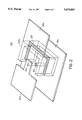
- FIG. 1 is a three-dimensional view of an integrated circuit interlevel conductor defect characterization test structure system
- FIG. 2 is an enlarged perspective view of one of the test structures of FIG. 1;
- FIG. 3 is a schematic view of an integrated circuit interlevel conductor defect characterization test structure as shown in FIG. 2 illustrating the current flow through the input interlevel conductor under test in the absence of any defect;
- FIG. 4 is a view similar to FIG. 3 showing the redistribution of the current flow of the input interlevel conductor with a defect present;
- FIG. 5 is a view similar to FIG. 2 showing an alternative construction for the input interlevel conductor
- FIG. 6 is a view similar to FIG. 6 in which the conductor layer includes a plurality of conductor sections, one associated with each test structure;
- FIGS. 7A-7C are schematic illustrations of alternative forms of the input interlevel conductor and the interlevel conductor under test.
- FIG. 1 An integrated circuit interlevel conductor defect characterization test structure system 10 according to this invention including a plurality of individual test structures 12, each of which includes an interlevel conductor 14 formed by a plated or filled (in this example, filled) through-hole through insulating layer 16 extending to and in electrical contact with conductive layer 18. Interlevel conductor 14 is connected with contact pad 20. Surrounding interlevel conductor 14 under test is input interlevel conductor 22 which is shown as generally U-shaped. Interlevel conductor 22 also extends through insulating layer 16 and makes electrical contact with conductor layer 18. Interlevel conductor 22 is also a through-hole in the shape of a U and is filled to effect the interlevel conductor. Interlevel conductor 22 is connected to contact pad 24.
- interlevel conductor 14 formed by a plated or filled (in this example, filled) through-hole through insulating layer 16 extending to and in electrical contact with conductive layer 18.
- Interlevel conductor 14 is connected with contact pad 20.
- Surrounding interlevel conductor 14 under test is input interlevel conduct
- a meter such as ohmmeter 26 has its probe 28 and 30 connected to pads 20 and 24, respectively, to measure the resistance in the test circuit between contact pad 24, input interlevel conductor 22, conductor layer 18, the interlevel conductor 14 under test, and contact pad 20. If it reads within a predetermined range then test structure 12 is considered to be without defect. If the measurement varies from the predetermined level then the test structure is determined to have a defect in the interlevel conductor 14 under test. With test structure 12, a reading which deviates from the expected reading indicates a failure in a particular interlevel conductor, i.e., 14, not in input interlevel conductor 22 or in any other interlevel conductor.
- a single test structure 12a is better visualized with reference to FIG. 2, where it can be seen that the input interlevel conductor 22a at least partially surrounds interlevel conductor 14a which is under test.
- the conductor material that makes up interlevel conductor 14a under test and that makes up input interlevel conductor 22a.
- conductor 14a has a unit cross-sectional area 23
- conductor 25 has a cross-sectional area at least twice and preferably many times that of the unit cross-sectional area 23.
- unit cross-sectional area is meant any selected area arbitrarily chosen as a reference and typically dictated by the technology such as the standardized contact/via size for a CMOS fabrication technology:
- FIG. 3 The operation of the test circuit as shown in FIG. 1 for a single test structure is schematically depicted in FIG. 3, where input interlevel conductor 22b is shown as a flat planar shape as opposed to the U shape of FIGS. 1 and 2.
- current 30 introduced into input interlevel electrode 22b flows down through it and across conductor layer 18b into interlevel electrode 14b which is under test.
- Input interlevel electrode 22b is substantially greater in cross-sectional area than is interlevel electrode 14b . That is, it is at least twice as large in cross-sectional area and is typically an order of magnitude or even two orders of magnitude greater than the cross-sectional area of interlevel conductor 14b .
- interlevel electrode 22 has been shown as a solid U-shaped conductor, this is not necessarily so. As shown in FIG. 5, it may be a hollow conductor plated as may interlevel electrode 14 under test, and interlevel electrode 22 may be comprised of a number of individual cylindrical conductors 22c, for example, where each of those is a unit area.
- conductor layer 18 is shown as a single layer which serves all of the test structures, this is not a necessary limitation of the invention.
- conductor layer 18d, FIG. 6, may include a plurality of conductor sections 18e, one associated with each of the test structures 12e.
- input interlevel conductor 14f under test may be confronted with an input interlevel conductor 22f which is semicircular in shape, FIG. 7A, arranged so that every point on conductor 22f is equidistant from conductor 14f.
- input interlevel electrode 22g may be of flat planar linear nowadays construction.
- input interlevel electrode 22h may be more nearly fully circular in shape and again may be positioned so that every point on it is equidistant from interlevel electrode 14h under test.
Abstract
An interlevel conductor defect characterization integrated circuit test structure including first and second spaced test pads, a conductor layer, an insulator layer between the conductor layer and the test pads; and a first interlevel conductor having a unit cross-sectional conductive area extending between the first test pad and the conductor layer, and a second interlevel conductor extending between said second test pad and said conductor layer and having a cross-sectional conductive area substantially greater than the unit area for detecting defects which restrict the current carrying capacity of said unit area of the first interlevel conductor but not the second interlevel conductor.
Description
This invention relates to an integrated circuit interlevel conductor defect characterization test structure, and more particularly to a plurality of such test structures used in a system to determine the actual number of interlevel conductor failures.
Yield prediction and yield estimation are very important considerations in integrated circuit design and process development. Models exist for predicting yield, which is the number of expected good chips on a wafer to the total number of chips on the wafer; however, the accuracy of such models depends on the accuracy of the information that describes contact and via defects. Contacts and vias are the interlevel conductors between the conduction layers of an integrated circuit (IC) chip. Contacts generally refer to those between metal layers and poly or diffusion layers. Vias refer to the interlevel conductors between metal and metal. With the increase in the complexity and number of layers in IC chips the detection of flaws in the interlevel conductors has become more important in the estimation of yield.
Presently IC chip interlevel conductor test structures employ a contact or via "chain". The chain is constructed in an IC chip with a number of independent metal sections on a first layer and a number of independent metal, poly or diffusion sections on a second layer spaced from the first layer by an insulating layer. Each section on the first layer is interconnected with a section on the second layer by an interlevel conductor so that there is a series path or "chain" from a first layer section through an interlevel conductor back to another section on the first layer and through yet another interlevel conductor to yet another sector on the second layer and so on. A measurement taken between the beginning and end of the chain indicates the resistance from one end of the chain to the other. Any rise in the normal resistance in that chain indicates a defect in one of the interlevel conductors or in the connecting sections. While this "chain" approach does indicate when there is a problem it does not distinguish between defects in the interlevel conductors and defects in the sections and there is no way to quantify the defects, e.g., how many interlevel conductors failed: one, two, one hundred. And so there is no way to quantify the yield loss due to interlevel conductor failure. Yield loss at interlevel conductors or the failure rate of interlevel conductors due to defects in the test structure is necessary to predict yield loss at interlevel conductors for other IC products.
It is therefore an object of this invention to provide an integrated circuit interlevel conductor defect characterization test structure and system.
It is a further object of this invention to provide such a defect characterization structure and system which enables yield rate estimation for other IC products.
It is a further object of this invention to provide such a defect characterization structure and system which enables measurement of the interlevel conductor defect rate for the technology as well.
It is a further object of this invention to provide such a defect characterization structure and system which renders a sufficiently large sample size for reliable statistical prediction.
It is a further object of this invention to provide such a defect characterization structure and system which identifies individual interlevel conductor failures.
It is a further object of this invention to provide such a defect characterization structure and system which is simpler and easier to fabricate.
It is a further object of this invention to provide such a defect characterization structure and system which can employ a single unpatterned return conductor layer.
It is a further object of this invention to provide such a defect characterization structure and system which ensures that only the defects in a standard unit cross-sectional area interlevel conductor will effect the measurement.
The invention results from the realization that a truly quantifiable measure of interlevel conductor defects in IC chips can be achieved by employing a test structure in which a test circuit is created between a pair of interlevel conductors connected in series where one such interlevel conductor is a unit cross-sectional area and the other is at least twice as large so that defects which cause a failure in the unit area interlevel conductor will not interfere with the functioning of the larger area interlevel conductor.
This invention features an interlevel conductor defect characterization integrated circuit test structure including first and second spaced test pads, a conductor layer, and an insulator layer between the conductor layer and the test pads. There are a first interlevel unit conductor having a unit cross-sectional conductive area extending between the first test pad and the conductor layer, and a second interlevel conductor extending between said second test pad and said conductor layer and having a cross-sectional conductive area substantially greater than the unit area for detecting defects which restrict the current carrying capacity of said unit area of the first interlevel conductor but not the second interlevel conductor.
In a preferred embodiment the cross-sectional area of the second interlevel conductor may be at least twice that of the unit area. The second interlevel conductor may at least partially surround the first interlevel conductor and may at all points be equidistant from the first interlevel conductor.
The invention also features an integrated circuit interlevel conductor defect quantifiable test structure system including a plurality of test structures. Each test structure may include first and second spaced test pads, a conductor layer, and an insulator layer between the conductor layer and the test pads. There may be a first interlevel conductor having a unit cross-sectional conductive area extending between the first test pad and the conductor layer, and a second interlevel conductor having a cross-sectional conductive area substantially greater than the unit area for detecting defects which restrict the current carrying capacity of the unit area of the first interlevel conductor but not the second interlevel conductor.
In a preferred embodiment the conductor layer may include a plurality of independent sections each associated with a pair of first and second test probes.
Other objects, features and advantages will occur to those skilled in the art from the following description of a preferred embodiment and the accompanying drawings, in which:
FIG. 1 is a three-dimensional view of an integrated circuit interlevel conductor defect characterization test structure system;
FIG. 2 is an enlarged perspective view of one of the test structures of FIG. 1;
FIG. 3 is a schematic view of an integrated circuit interlevel conductor defect characterization test structure as shown in FIG. 2 illustrating the current flow through the input interlevel conductor under test in the absence of any defect;
FIG. 4 is a view similar to FIG. 3 showing the redistribution of the current flow of the input interlevel conductor with a defect present;
FIG. 5 is a view similar to FIG. 2 showing an alternative construction for the input interlevel conductor;
FIG. 6 is a view similar to FIG. 6 in which the conductor layer includes a plurality of conductor sections, one associated with each test structure; and
FIGS. 7A-7C are schematic illustrations of alternative forms of the input interlevel conductor and the interlevel conductor under test.
There is shown in FIG. 1 an integrated circuit interlevel conductor defect characterization test structure system 10 according to this invention including a plurality of individual test structures 12, each of which includes an interlevel conductor 14 formed by a plated or filled (in this example, filled) through-hole through insulating layer 16 extending to and in electrical contact with conductive layer 18. Interlevel conductor 14 is connected with contact pad 20. Surrounding interlevel conductor 14 under test is input interlevel conductor 22 which is shown as generally U-shaped. Interlevel conductor 22 also extends through insulating layer 16 and makes electrical contact with conductor layer 18. Interlevel conductor 22 is also a through-hole in the shape of a U and is filled to effect the interlevel conductor. Interlevel conductor 22 is connected to contact pad 24. A meter such as ohmmeter 26 has its probe 28 and 30 connected to pads 20 and 24, respectively, to measure the resistance in the test circuit between contact pad 24, input interlevel conductor 22, conductor layer 18, the interlevel conductor 14 under test, and contact pad 20. If it reads within a predetermined range then test structure 12 is considered to be without defect. If the measurement varies from the predetermined level then the test structure is determined to have a defect in the interlevel conductor 14 under test. With test structure 12, a reading which deviates from the expected reading indicates a failure in a particular interlevel conductor, i.e., 14, not in input interlevel conductor 22 or in any other interlevel conductor. In prior art devices, as indicated in the Background, the deviation from the nominal reading indicated only that there was a defect somewhere in the test structure system but there was no indication of where it was or how many interlevel conductors, i.e., vias or contacts were actually subject to defects.
A single test structure 12a is better visualized with reference to FIG. 2, where it can be seen that the input interlevel conductor 22a at least partially surrounds interlevel conductor 14a which is under test. For simplicity, in FIG. 2 all that is shown is the conductor material that makes up interlevel conductor 14a under test and that makes up input interlevel conductor 22a. There conductor 14a has a unit cross-sectional area 23 whereas conductor 25 has a cross-sectional area at least twice and preferably many times that of the unit cross-sectional area 23. By unit cross-sectional area is meant any selected area arbitrarily chosen as a reference and typically dictated by the technology such as the standardized contact/via size for a CMOS fabrication technology:
The operation of the test circuit as shown in FIG. 1 for a single test structure is schematically depicted in FIG. 3, where input interlevel conductor 22b is shown as a flat planar shape as opposed to the U shape of FIGS. 1 and 2. There it can be seen that current 30 introduced into input interlevel electrode 22b flows down through it and across conductor layer 18b into interlevel electrode 14b which is under test. Input interlevel electrode 22b is substantially greater in cross-sectional area than is interlevel electrode 14b . That is, it is at least twice as large in cross-sectional area and is typically an order of magnitude or even two orders of magnitude greater than the cross-sectional area of interlevel conductor 14b . If this is so then a defect which would interrupt the current flow in interlevel electrode 14b will not interrupt the current flow in input interlevel conductor 22b . In fact, preferably it will hardly be detectable. This is done so that the only defects that will be detected by the measurement will be the defects that occur in the interlevel conductor 14 under test. Thus any deviation from the nominal or expected reading must come from a defect in the interlevel conductor 14b under test and will not be contributed to by any defects that may have occurred in the input interlevel electrode 22b.
This can be seen more clearly in FIG. 4, where a defect 40 has been introduced in interlevel electrode 14b of unit cross-sectional area under test so that the current 30 is stopped and cannot flow beyond defect 40. However, a defect of the same size 40' in input interlevel conductor 22b has virtually no effect on the current flow through conductor 22b because conductor 22b has a cross-sectional area 25b of many times the cross-sectional area 23b of conductor 14b. The current simply splits into a number of paths and distributes itself around defect 40' so that there is no significant decrease of the current or apparent increase in resistance due to the defect 40' which in interlevel electrode 14b would completely cut off the current flow.
Although thus far interlevel electrode 22 has been shown as a solid U-shaped conductor, this is not necessarily so. As shown in FIG. 5, it may be a hollow conductor plated as may interlevel electrode 14 under test, and interlevel electrode 22 may be comprised of a number of individual cylindrical conductors 22c, for example, where each of those is a unit area.
Although thus far in FIG. 1 conductor layer 18 is shown as a single layer which serves all of the test structures, this is not a necessary limitation of the invention. For example, conductor layer 18d, FIG. 6, may include a plurality of conductor sections 18e, one associated with each of the test structures 12e.
Although thus far the input interlevel conductor is shown as a U-shaped or C-shaped element, this is not a necessary limitation of the invention. For example, as shown in FIG. 7A, interlevel conductor 14f under test may be confronted with an input interlevel conductor 22f which is semicircular in shape, FIG. 7A, arranged so that every point on conductor 22f is equidistant from conductor 14f. Or, alternatively, as shown in FIG. 7B, input interlevel electrode 22g may be of flat planar linear?! construction. Alternatively, input interlevel electrode 22h may be more nearly fully circular in shape and again may be positioned so that every point on it is equidistant from interlevel electrode 14h under test.
Although specific features of this invention are shown in some drawings and not others, this is for convenience only as each feature may be combined with any or all of the other features in accordance with the invention.
Other embodiments will occur to those skilled in the art and are within the following claims:
Claims (6)
1. An interlevel conductor defect characterization integrated circuit test structure comprising:
first and second spaced test pads;
a conductor layer;
an insulator layer between said conductor layer and said test pads; and
a first interlevel unit conductor having a unit cross-sectional conductive area extending between said first test pad and said conductor layer, and a second interlevel conductor extending between said second test pad and said conductor layer and having a cross-sectional conductive area substantially greater than said unit area for detecting defects which restrict the current carrying capacity of said unit area of said first interlevel conductor but not said second interlevel conductor.
2. The interlevel conductor defect characterization integrated circuit test structure of claim 1 in which said cross-sectional area of said second interlevel conductor is at least twice that of said unit area.
3. The interlevel conductor defect quantifiable integrated circuit test structure of claim 1 in which said second interlevel conductor at least partially surrounds said first interlevel conductor.
4. The interlevel conductor defect characterization integrated circuit test structure of claim 1 in which said second interlevel conductor is at all points equidistant from said first interlevel conductor.
5. An integrated circuit interlevel conductor defect characterization test structure system comprising:
a plurality of test structures each including:
first and second spaced test pads;
a conductor layer;
an insulator layer between said conductor layer and said test pads; and
a first interlevel unit conductor having a unit cross-sectional conductive area extending between said first test pad and said conductor layer, and a second interlevel conductor extending between said second test pad and said conductor layer and having a cross-sectional conductive area substantially greater than said unit area for detecting defects which restrict the current carrying capacity of said unit area of said first interlevel conductor but not said second interlevel conductor.
6. The integrated circuit interlevel conductor defect quantifiable test structure of claim 5 in which said conductor substrate includes a plurality of independent sections each associated with a pair of first and second test probes.
Priority Applications (1)
| Application Number | Priority Date | Filing Date | Title |
|---|---|---|---|
| US08/560,650 US5670883A (en) | 1995-11-20 | 1995-11-20 | Integrated circuit interlevel conductor defect characterization test structure and system |
Applications Claiming Priority (1)
| Application Number | Priority Date | Filing Date | Title |
|---|---|---|---|
| US08/560,650 US5670883A (en) | 1995-11-20 | 1995-11-20 | Integrated circuit interlevel conductor defect characterization test structure and system |
Publications (1)
| Publication Number | Publication Date |
|---|---|
| US5670883A true US5670883A (en) | 1997-09-23 |
Family
ID=24238717
Family Applications (1)
| Application Number | Title | Priority Date | Filing Date |
|---|---|---|---|
| US08/560,650 Expired - Lifetime US5670883A (en) | 1995-11-20 | 1995-11-20 | Integrated circuit interlevel conductor defect characterization test structure and system |
Country Status (1)
| Country | Link |
|---|---|
| US (1) | US5670883A (en) |
Cited By (3)
| Publication number | Priority date | Publication date | Assignee | Title |
|---|---|---|---|---|
| US20020079883A1 (en) * | 2000-12-13 | 2002-06-27 | Beech Clive David | Integrated circuit test structure |
| US6844751B2 (en) | 2000-09-30 | 2005-01-18 | Texas Instruments Incorporated | Multi-state test structures and methods |
| US8793547B2 (en) * | 2013-01-02 | 2014-07-29 | Altera Corporation | 3D built-in self-test scheme for 3D assembly defect detection |
Citations (6)
| Publication number | Priority date | Publication date | Assignee | Title |
|---|---|---|---|---|
| US3859711A (en) * | 1973-03-20 | 1975-01-14 | Ibm | Method of detecting misregistration of internal layers of a multilayer printed circuit panel |
| US4144493A (en) * | 1976-06-30 | 1979-03-13 | International Business Machines Corporation | Integrated circuit test structure |
| US4672314A (en) * | 1985-04-12 | 1987-06-09 | Rca Corporation | Comprehensive semiconductor test structure |
| US4835466A (en) * | 1987-02-06 | 1989-05-30 | Fairchild Semiconductor Corporation | Apparatus and method for detecting spot defects in integrated circuits |
| US5049811A (en) * | 1990-07-02 | 1991-09-17 | Motorola, Inc. | Measuring integrity of semiconductor multi-layer metal structures |
| US5326428A (en) * | 1993-09-03 | 1994-07-05 | Micron Semiconductor, Inc. | Method for testing semiconductor circuitry for operability and method of forming apparatus for testing semiconductor circuitry for operability |
-
1995
- 1995-11-20 US US08/560,650 patent/US5670883A/en not_active Expired - Lifetime
Patent Citations (7)
| Publication number | Priority date | Publication date | Assignee | Title |
|---|---|---|---|---|
| US3859711A (en) * | 1973-03-20 | 1975-01-14 | Ibm | Method of detecting misregistration of internal layers of a multilayer printed circuit panel |
| US4144493A (en) * | 1976-06-30 | 1979-03-13 | International Business Machines Corporation | Integrated circuit test structure |
| US4672314A (en) * | 1985-04-12 | 1987-06-09 | Rca Corporation | Comprehensive semiconductor test structure |
| US4835466A (en) * | 1987-02-06 | 1989-05-30 | Fairchild Semiconductor Corporation | Apparatus and method for detecting spot defects in integrated circuits |
| US5051690A (en) * | 1987-02-06 | 1991-09-24 | National Semiconductor Corporation | Apparatus and method for detecting vertically propagated defects in integrated circuits |
| US5049811A (en) * | 1990-07-02 | 1991-09-17 | Motorola, Inc. | Measuring integrity of semiconductor multi-layer metal structures |
| US5326428A (en) * | 1993-09-03 | 1994-07-05 | Micron Semiconductor, Inc. | Method for testing semiconductor circuitry for operability and method of forming apparatus for testing semiconductor circuitry for operability |
Cited By (4)
| Publication number | Priority date | Publication date | Assignee | Title |
|---|---|---|---|---|
| US6844751B2 (en) | 2000-09-30 | 2005-01-18 | Texas Instruments Incorporated | Multi-state test structures and methods |
| US20020079883A1 (en) * | 2000-12-13 | 2002-06-27 | Beech Clive David | Integrated circuit test structure |
| US6809540B2 (en) * | 2000-12-13 | 2004-10-26 | Zarlink Semiconductor Limited | Integrated circuit test structure |
| US8793547B2 (en) * | 2013-01-02 | 2014-07-29 | Altera Corporation | 3D built-in self-test scheme for 3D assembly defect detection |
Similar Documents
| Publication | Publication Date | Title |
|---|---|---|
| US5514974A (en) | Test device and method for signalling metal failure of semiconductor wafer | |
| US7081758B2 (en) | Inspection pattern, inspection method, and inspection system for detection of latent defect of multi-layer wiring structure | |
| US7719302B2 (en) | On-chip electromigration monitoring | |
| US7105856B1 (en) | Test key having a chain circuit and a kelvin structure | |
| US6577149B2 (en) | Method and device for addressable failure site test structure | |
| US7132684B2 (en) | Test structure for detecting defect size in a semiconductor device and test method using same | |
| US7365529B2 (en) | Test structure design for reliability test | |
| US5670883A (en) | Integrated circuit interlevel conductor defect characterization test structure and system | |
| US8836342B2 (en) | Test structure for highly accelerated electromigration tests for thick metallization systems of solid state integrated circuits | |
| US5528151A (en) | Thermal fatigue testing using plural test trips with graduated sizing and recessed anchoring | |
| KR20090014867A (en) | Semiconductor device having contact failure detector | |
| US6989682B1 (en) | Test key on a wafer | |
| US7119545B2 (en) | Capacitive monitors for detecting metal extrusion during electromigration | |
| US20020063249A1 (en) | Kerf contact to silicon redesign for defect isolation and analysis | |
| US6819124B1 (en) | Detection of electromigration in integrated circuits | |
| KR100295916B1 (en) | Test Structure and Method for Measuring Minimum Area Design Rule | |
| US20020078409A1 (en) | Method and system for detecting an outlying resistance in a plurality of resistive elements | |
| CN110620058B (en) | Electromigration reliability test structure and electromigration reliability test method | |
| JP2004022570A (en) | Semiconductor device containing evaluating element and failure analyzing method using the evaluating element | |
| JP2006189340A (en) | Inspection system and inspection method for semiconductor device | |
| JPH07130815A (en) | Semiconductor device and evaluation thereof | |
| KR20010063430A (en) | A metal line electromigration test pattern in a semiconductor device and Method of testing the same | |
| JP2007012709A (en) | Semiconductor inspection device, and inspection method of semiconductor device | |
| JPH10300823A (en) | Prober inspection method | |
| JP2007024719A (en) | Evaluation method of semiconductor device |
Legal Events
| Date | Code | Title | Description |
|---|---|---|---|
| AS | Assignment |
Owner name: ANALOG DEVICES, INC., MASSACHUSETTS Free format text: ASSIGNMENT OF ASSIGNORS INTEREST;ASSIGNORS:O'DONOGHUE, GEOFF;MUNROE, SCOTT C.;REEL/FRAME:007789/0381 Effective date: 19951117 |
|
| STCF | Information on status: patent grant |
Free format text: PATENTED CASE |
|
| FPAY | Fee payment |
Year of fee payment: 4 |
|
| FPAY | Fee payment |
Year of fee payment: 8 |
|
| FPAY | Fee payment |
Year of fee payment: 12 |