US5662877A - Process for forming diamond-like thin film - Google Patents
Process for forming diamond-like thin film Download PDFInfo
- Publication number
- US5662877A US5662877A US07/827,853 US82785392A US5662877A US 5662877 A US5662877 A US 5662877A US 82785392 A US82785392 A US 82785392A US 5662877 A US5662877 A US 5662877A
- Authority
- US
- United States
- Prior art keywords
- diamond
- substrate
- forming
- thin film
- grid
- Prior art date
- Legal status (The legal status is an assumption and is not a legal conclusion. Google has not performed a legal analysis and makes no representation as to the accuracy of the status listed.)
- Expired - Lifetime
Links
- 238000000034 method Methods 0.000 title claims abstract description 41
- 239000010409 thin film Substances 0.000 title claims description 33
- 239000000758 substrate Substances 0.000 claims abstract description 67
- 239000007789 gas Substances 0.000 claims abstract description 44
- 150000002500 ions Chemical class 0.000 claims abstract description 23
- 239000004215 Carbon black (E152) Substances 0.000 claims abstract description 16
- 229930195733 hydrocarbon Natural products 0.000 claims abstract description 16
- XKRFYHLGVUSROY-UHFFFAOYSA-N Argon Chemical compound [Ar] XKRFYHLGVUSROY-UHFFFAOYSA-N 0.000 claims abstract description 14
- 239000000919 ceramic Substances 0.000 claims abstract description 12
- 239000011521 glass Substances 0.000 claims abstract description 11
- -1 hydrocarbon ions Chemical class 0.000 claims abstract description 10
- 229910052786 argon Inorganic materials 0.000 claims abstract description 9
- 239000010408 film Substances 0.000 claims description 26
- 150000002430 hydrocarbons Chemical class 0.000 claims description 11
- 229910045601 alloy Inorganic materials 0.000 claims description 8
- 239000000956 alloy Substances 0.000 claims description 8
- XEEYBQQBJWHFJM-UHFFFAOYSA-N iron Substances [Fe] XEEYBQQBJWHFJM-UHFFFAOYSA-N 0.000 claims description 8
- IJGRMHOSHXDMSA-UHFFFAOYSA-N Atomic nitrogen Chemical compound N#N IJGRMHOSHXDMSA-UHFFFAOYSA-N 0.000 claims description 6
- 239000001257 hydrogen Substances 0.000 claims description 6
- 229910052739 hydrogen Inorganic materials 0.000 claims description 6
- 238000006243 chemical reaction Methods 0.000 claims description 5
- 229910052742 iron Inorganic materials 0.000 claims description 5
- 229910052734 helium Inorganic materials 0.000 claims description 4
- 239000000463 material Substances 0.000 claims description 4
- 238000000354 decomposition reaction Methods 0.000 claims description 3
- 239000001307 helium Substances 0.000 claims description 3
- SWQJXJOGLNCZEY-UHFFFAOYSA-N helium atom Chemical compound [He] SWQJXJOGLNCZEY-UHFFFAOYSA-N 0.000 claims description 3
- 229910052754 neon Inorganic materials 0.000 claims description 3
- GKAOGPIIYCISHV-UHFFFAOYSA-N neon atom Chemical compound [Ne] GKAOGPIIYCISHV-UHFFFAOYSA-N 0.000 claims description 3
- 229910052759 nickel Inorganic materials 0.000 claims description 3
- 229910052757 nitrogen Inorganic materials 0.000 claims description 3
- PXHVJJICTQNCMI-UHFFFAOYSA-N nickel Substances [Ni] PXHVJJICTQNCMI-UHFFFAOYSA-N 0.000 claims description 2
- 125000004435 hydrogen atom Chemical class [H]* 0.000 claims 1
- 238000006386 neutralization reaction Methods 0.000 claims 1
- 230000001070 adhesive effect Effects 0.000 abstract description 14
- 229910052751 metal Inorganic materials 0.000 abstract description 8
- 239000002184 metal Substances 0.000 abstract description 8
- 230000008021 deposition Effects 0.000 abstract description 4
- 230000005684 electric field Effects 0.000 abstract description 4
- VNWKTOKETHGBQD-UHFFFAOYSA-N methane Chemical compound C VNWKTOKETHGBQD-UHFFFAOYSA-N 0.000 description 13
- LFQSCWFLJHTTHZ-UHFFFAOYSA-N Ethanol Chemical compound CCO LFQSCWFLJHTTHZ-UHFFFAOYSA-N 0.000 description 6
- 230000007547 defect Effects 0.000 description 5
- 229910003460 diamond Inorganic materials 0.000 description 5
- 239000010432 diamond Substances 0.000 description 5
- CSCPPACGZOOCGX-UHFFFAOYSA-N Acetone Chemical compound CC(C)=O CSCPPACGZOOCGX-UHFFFAOYSA-N 0.000 description 4
- CURLTUGMZLYLDI-UHFFFAOYSA-N Carbon dioxide Chemical compound O=C=O CURLTUGMZLYLDI-UHFFFAOYSA-N 0.000 description 4
- 238000000151 deposition Methods 0.000 description 4
- 230000000694 effects Effects 0.000 description 4
- 238000010884 ion-beam technique Methods 0.000 description 4
- 150000002739 metals Chemical class 0.000 description 4
- ZWEHNKRNPOVVGH-UHFFFAOYSA-N 2-Butanone Chemical compound CCC(C)=O ZWEHNKRNPOVVGH-UHFFFAOYSA-N 0.000 description 3
- 229910001209 Low-carbon steel Inorganic materials 0.000 description 3
- OKKJLVBELUTLKV-UHFFFAOYSA-N Methanol Chemical compound OC OKKJLVBELUTLKV-UHFFFAOYSA-N 0.000 description 3
- HEMHJVSKTPXQMS-UHFFFAOYSA-M Sodium hydroxide Chemical compound [OH-].[Na+] HEMHJVSKTPXQMS-UHFFFAOYSA-M 0.000 description 3
- 238000005260 corrosion Methods 0.000 description 3
- 230000002950 deficient Effects 0.000 description 3
- 238000005530 etching Methods 0.000 description 3
- 235000019441 ethanol Nutrition 0.000 description 3
- 150000002431 hydrogen Chemical class 0.000 description 3
- 238000005406 washing Methods 0.000 description 3
- XLYOFNOQVPJJNP-UHFFFAOYSA-N water Substances O XLYOFNOQVPJJNP-UHFFFAOYSA-N 0.000 description 3
- 229910001868 water Inorganic materials 0.000 description 3
- 229910018404 Al2 O3 Inorganic materials 0.000 description 2
- UGFAIRIUMAVXCW-UHFFFAOYSA-N Carbon monoxide Chemical compound [O+]#[C-] UGFAIRIUMAVXCW-UHFFFAOYSA-N 0.000 description 2
- ATUOYWHBWRKTHZ-UHFFFAOYSA-N Propane Chemical compound CCC ATUOYWHBWRKTHZ-UHFFFAOYSA-N 0.000 description 2
- 239000001569 carbon dioxide Substances 0.000 description 2
- 229910002092 carbon dioxide Inorganic materials 0.000 description 2
- 229910002091 carbon monoxide Inorganic materials 0.000 description 2
- 230000000052 comparative effect Effects 0.000 description 2
- 230000007423 decrease Effects 0.000 description 2
- 230000004907 flux Effects 0.000 description 2
- 239000007792 gaseous phase Substances 0.000 description 2
- 239000002075 main ingredient Substances 0.000 description 2
- 230000007935 neutral effect Effects 0.000 description 2
- 239000002245 particle Substances 0.000 description 2
- 239000000126 substance Substances 0.000 description 2
- OTMSDBZUPAUEDD-UHFFFAOYSA-N Ethane Chemical compound CC OTMSDBZUPAUEDD-UHFFFAOYSA-N 0.000 description 1
- 229910000760 Hardened steel Inorganic materials 0.000 description 1
- UFHFLCQGNIYNRP-UHFFFAOYSA-N Hydrogen Chemical compound [H][H] UFHFLCQGNIYNRP-UHFFFAOYSA-N 0.000 description 1
- 230000002411 adverse Effects 0.000 description 1
- HSFWRNGVRCDJHI-UHFFFAOYSA-N alpha-acetylene Natural products C#C HSFWRNGVRCDJHI-UHFFFAOYSA-N 0.000 description 1
- PNEYBMLMFCGWSK-UHFFFAOYSA-N aluminium oxide Inorganic materials [O-2].[O-2].[O-2].[Al+3].[Al+3] PNEYBMLMFCGWSK-UHFFFAOYSA-N 0.000 description 1
- QVGXLLKOCUKJST-UHFFFAOYSA-N atomic oxygen Chemical compound [O] QVGXLLKOCUKJST-UHFFFAOYSA-N 0.000 description 1
- 230000009286 beneficial effect Effects 0.000 description 1
- 229910052799 carbon Inorganic materials 0.000 description 1
- 239000012159 carrier gas Substances 0.000 description 1
- 229910052804 chromium Inorganic materials 0.000 description 1
- 238000004140 cleaning Methods 0.000 description 1
- 238000010276 construction Methods 0.000 description 1
- 239000013078 crystal Substances 0.000 description 1
- 238000005137 deposition process Methods 0.000 description 1
- 239000003599 detergent Substances 0.000 description 1
- 238000009792 diffusion process Methods 0.000 description 1
- 238000010891 electric arc Methods 0.000 description 1
- 238000005516 engineering process Methods 0.000 description 1
- 239000003822 epoxy resin Substances 0.000 description 1
- 125000002534 ethynyl group Chemical group [H]C#C* 0.000 description 1
- 230000005284 excitation Effects 0.000 description 1
- 238000000227 grinding Methods 0.000 description 1
- 239000012535 impurity Substances 0.000 description 1
- 239000011810 insulating material Substances 0.000 description 1
- 150000002576 ketones Chemical class 0.000 description 1
- 238000004519 manufacturing process Methods 0.000 description 1
- 239000013081 microcrystal Substances 0.000 description 1
- 230000001590 oxidative effect Effects 0.000 description 1
- 239000001301 oxygen Substances 0.000 description 1
- 229910052760 oxygen Inorganic materials 0.000 description 1
- 229920000647 polyepoxide Polymers 0.000 description 1
- 239000001294 propane Substances 0.000 description 1
- 229930195734 saturated hydrocarbon Natural products 0.000 description 1
- 238000002791 soaking Methods 0.000 description 1
- 238000000992 sputter etching Methods 0.000 description 1
- 239000010935 stainless steel Substances 0.000 description 1
- 229910001220 stainless steel Inorganic materials 0.000 description 1
- 239000007858 starting material Substances 0.000 description 1
- 230000003746 surface roughness Effects 0.000 description 1
- 229930195735 unsaturated hydrocarbon Natural products 0.000 description 1
Images


Classifications
-
- C—CHEMISTRY; METALLURGY
- C23—COATING METALLIC MATERIAL; COATING MATERIAL WITH METALLIC MATERIAL; CHEMICAL SURFACE TREATMENT; DIFFUSION TREATMENT OF METALLIC MATERIAL; COATING BY VACUUM EVAPORATION, BY SPUTTERING, BY ION IMPLANTATION OR BY CHEMICAL VAPOUR DEPOSITION, IN GENERAL; INHIBITING CORROSION OF METALLIC MATERIAL OR INCRUSTATION IN GENERAL
- C23C—COATING METALLIC MATERIAL; COATING MATERIAL WITH METALLIC MATERIAL; SURFACE TREATMENT OF METALLIC MATERIAL BY DIFFUSION INTO THE SURFACE, BY CHEMICAL CONVERSION OR SUBSTITUTION; COATING BY VACUUM EVAPORATION, BY SPUTTERING, BY ION IMPLANTATION OR BY CHEMICAL VAPOUR DEPOSITION, IN GENERAL
- C23C16/00—Chemical coating by decomposition of gaseous compounds, without leaving reaction products of surface material in the coating, i.e. chemical vapour deposition [CVD] processes
- C23C16/02—Pretreatment of the material to be coated
- C23C16/0254—Physical treatment to alter the texture of the surface, e.g. scratching or polishing
- C23C16/0263—Irradiation with laser or particle beam
-
- C—CHEMISTRY; METALLURGY
- C23—COATING METALLIC MATERIAL; COATING MATERIAL WITH METALLIC MATERIAL; CHEMICAL SURFACE TREATMENT; DIFFUSION TREATMENT OF METALLIC MATERIAL; COATING BY VACUUM EVAPORATION, BY SPUTTERING, BY ION IMPLANTATION OR BY CHEMICAL VAPOUR DEPOSITION, IN GENERAL; INHIBITING CORROSION OF METALLIC MATERIAL OR INCRUSTATION IN GENERAL
- C23C—COATING METALLIC MATERIAL; COATING MATERIAL WITH METALLIC MATERIAL; SURFACE TREATMENT OF METALLIC MATERIAL BY DIFFUSION INTO THE SURFACE, BY CHEMICAL CONVERSION OR SUBSTITUTION; COATING BY VACUUM EVAPORATION, BY SPUTTERING, BY ION IMPLANTATION OR BY CHEMICAL VAPOUR DEPOSITION, IN GENERAL
- C23C16/00—Chemical coating by decomposition of gaseous compounds, without leaving reaction products of surface material in the coating, i.e. chemical vapour deposition [CVD] processes
- C23C16/22—Chemical coating by decomposition of gaseous compounds, without leaving reaction products of surface material in the coating, i.e. chemical vapour deposition [CVD] processes characterised by the deposition of inorganic material, other than metallic material
- C23C16/26—Deposition of carbon only
-
- C—CHEMISTRY; METALLURGY
- C30—CRYSTAL GROWTH
- C30B—SINGLE-CRYSTAL GROWTH; UNIDIRECTIONAL SOLIDIFICATION OF EUTECTIC MATERIAL OR UNIDIRECTIONAL DEMIXING OF EUTECTOID MATERIAL; REFINING BY ZONE-MELTING OF MATERIAL; PRODUCTION OF A HOMOGENEOUS POLYCRYSTALLINE MATERIAL WITH DEFINED STRUCTURE; SINGLE CRYSTALS OR HOMOGENEOUS POLYCRYSTALLINE MATERIAL WITH DEFINED STRUCTURE; AFTER-TREATMENT OF SINGLE CRYSTALS OR A HOMOGENEOUS POLYCRYSTALLINE MATERIAL WITH DEFINED STRUCTURE; APPARATUS THEREFOR
- C30B25/00—Single-crystal growth by chemical reaction of reactive gases, e.g. chemical vapour-deposition growth
- C30B25/02—Epitaxial-layer growth
-
- C—CHEMISTRY; METALLURGY
- C30—CRYSTAL GROWTH
- C30B—SINGLE-CRYSTAL GROWTH; UNIDIRECTIONAL SOLIDIFICATION OF EUTECTIC MATERIAL OR UNIDIRECTIONAL DEMIXING OF EUTECTOID MATERIAL; REFINING BY ZONE-MELTING OF MATERIAL; PRODUCTION OF A HOMOGENEOUS POLYCRYSTALLINE MATERIAL WITH DEFINED STRUCTURE; SINGLE CRYSTALS OR HOMOGENEOUS POLYCRYSTALLINE MATERIAL WITH DEFINED STRUCTURE; AFTER-TREATMENT OF SINGLE CRYSTALS OR A HOMOGENEOUS POLYCRYSTALLINE MATERIAL WITH DEFINED STRUCTURE; APPARATUS THEREFOR
- C30B29/00—Single crystals or homogeneous polycrystalline material with defined structure characterised by the material or by their shape
- C30B29/02—Elements
- C30B29/04—Diamond
Definitions
- the present invention relates to a process for forming a diamond or diamond-like thin film, and more particularly it relates to a film forming technique which improves the adhesive property or the bonding strength of a diamond or diamond-like thin film to a substrate.
- a diamond or diamond-like thin film (hereinafter called diamond-like thin film) produced by a gaseous phase method is superior in hardness, wear-resistance, durability, anti-chemical property, anti-corrosion property and as it can be adhered on a substrate of any shape, it is useful or believed to be hopeful as a protection film for an object which requires one or more of these properties.
- a diamond-like thin film can cover an object with any shape to be protected and is widely used as a protection film for anti-corrosion or wear-resistance, etc.
- diamond-like thin films produced by these prior methods have a poor bonding strength to a substrate depending on the kind of substrate and is easily peeled off from a substrate by an external force because these diamond-like thin films consist of an ensemble of micro crystals which is a cause of a large surface roughness. Therefore, their superior properties are not fully utilized in applications as protection films which require anti-corrosion property, wear-resistance property and the like. It is particularly known that iron or its alloys (e.g. mild steel (STC), stainless steel, hardened steel (SKD, SKS, etc.)), other metals or alloys such as Co, Ni and the like or their alloys, glass, ceramics, etc. have a poor bonding strength to a diamond-like thin film.
- STC mild steel
- SKS hardened steel
- Examples of substrates made of iron as a chief element are mold, grinding material, etc. which have a highest industrial value, while substrates made of glass or ceramics are used for a moving part of a thermal head etc. As it is used for many purposes, it is very important to improve the adhesive property of a diamond-like thin film to a substrate on which it is formed.
- a preliminary treatment to the substrate is proposed in Japanese Patent Application Public Disclosure Nos. 200898/1985, 204695/1985 and 174376/1986.
- Patent Application Public Disclosure No. 200898/1985 a diamond-like thin film is bonded to a substrate of a Co-WC alloy as a high hardness film and to this end it is proposed to pretreat the substrate by ion etching, using a glow discharge of direct current or alternating current directly to the surface of the substrate.
- the purpose is to increase the film-forming speed by increasing growing nuclei of diamond crystals, but, from the viewpoint of improvement of the adhesive property, the etching efficiency is not sufficiently high as an accelerating voltage is not applied, and the purpose of the present invention aiming at improvement of the adhesive property is, therefore, not attained sufficiently.
- Patent Application Public Disclosure No. 204695/1985 aiming at improvement of the film-forming speed proposes to introduce Ar gas into a vacuum chamber and forms a plasma by applying a voltage between an anode and a cathode to treat the substrate.
- the etching effect is small due to a low ion density of the plasma and, moreover, there is a problem in this process as will be described in the following in that the ions can be used only when the substrate is a metal and when a voltage can be applied to the substrate, while the present invention can be applicable to an insulating material such as glass and ceramics.
- the present invention attains the above mentioned purposes in a process for forming a diamond-like thin film on the surface of a substrate selected from a group of metals and alloys containing at least one of Co, Ni and Fe, ceramics and glass which have a poor affinity to said diamond-like thin film, by adopting a preliminary process, which comprises, prior to ionized deposition, disposing said substrate in a vacuum chamber of a film-forming apparatus, introducing into said vacuum chamber a bombardment gas, forming a stream of ions by ionizing means which consists of a thermal filament cathode and an anode surrounding the cathode, and accelerating the resulting stream by a grid which is at a lower potential than said anode to bombard the surface of the substrate.
- the prime merits of the preliminary process according to the present invention are that a bonding strength between the film and the substrate can be improved and moreover that a pretreatment process and then a diamond film-forming process can be carried out successively using the same apparatus with little changes of conditions.
- the reason why the effects of the present invention can be obtained is not clear, but it may be understood that oxided substances, unnecessary radicals and other smudges necessarily formed on the substrate surface in the air are removed, which improves the activity of the substrate surface.
- oxided substances, unnecessary radicals and other smudges necessarily formed on the substrate surface in the air are removed, which improves the activity of the substrate surface.
- SEM scanning electron microscope
- the present invention improves the adhesive property by pretreating under uniform conditions the substrate surface of metal, ceramics or glass etc. with a poor adhesive property, by accelerating ions under an electric field to the substrate in advance of a diamond-like film forming process.
- a diamond-like film forming process by ionized deposition uses thermal electron ionization means and an electric potential is applied to a grid to accelerate ionized hydrocarbon ions
- the present invention could attain the aimed purpose by ionizing and then accelerating a bombardment gas such as argon as a pretreatment process in the same apparatus.
- the ionized deposition process uses a hydrocarbon feed gas or a feed gas capable of producing a hydrocarbon upon decomposition or reaction.
- hydrocarbon is used to mean any of saturated hydrocarbons, such as methane, ethane, and propane, and unsaturated hydrocarbons, such as ethylene, propylene, and acetylene.
- the feed gas capable of producing a hydrocarbon on decomposition is an alcohol, such as methyl alcohol or ethyl alcohol, or a ketone, such as acetone or methyl ethyl ketone, or the like.
- the feed gas capable of producing a hydrocarbon gas on reaction is a mixed gas such as of carbon monoxide, carbon dioxide, and hydrogen or the like.
- the feed gas may contain at least one member of the family consisting of such rare gases as helium, neon, and argon, or hydrogen, oxygen, nitrogen, water, carbon monoxide, carbon dioxide, and the like.)
- the feed gas is ionized by arc discharge between a thermal filament cathode and an anode or by thermionic emission between a thermal filament cathode and an anode, and the resulting ion beam is accelerated by an electric field and directed to the substrate, whereby a diamond-like thin film is formed on the substrate.
- Japanese Patent Application Public Disclosure No. 174507/1984 Japanese Patent Application Nos.
- ionized deposition does not require such a high substrate temperature above 700° C. as are used in other processes.
- the process is also superior in that it achieves a high film-forming efficiency and that the resulting diamond-like film has good surface quality, high hardness, high heat transfer rate, high refractive index, etc., while eliminating the necessity of surface finish. Therefore, the present invention uses this process.
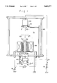
- FIG. 1 is a cross-sectional view illustrating an example of a diamond-like thin film producing apparatus of the present invention.
- FIG. 2 is a cross-sectional view illustrating another example of a diamond-like thin film producing apparatus.
- FIG. 3 is a perspective view illustrating a structure of filament part.
- FIG. 1 illustrates a preferred example of film-forming apparatus.
- the numeral 30 designates a vacuum vessel and 31 a chamber connected to an evacuation system 38 so that it can be evacuated to a high vacuum of about 10 -6 Torr.
- the numeral 32 indicates an electrode located at the back of a substrate S and kept at a negative potential Va.
- a mask 42 On the surface of the substrate S disposed close or touched is a mask 42 which has a window to regulate a shape or form of a diamond-like thin film. This mask may be contacted with the substrate, but to decrease cracks by thinning the thickness of the film periphery it is preferred to be separated.
- the numeral 33 indicates a grid to which the same potential Va is applied as to the substrate and is used to accelerate hydrocarbon ions in the process of film-forming.
- this grid 33 may be used a grid with a properly determined space ratio (an area of holes per unit area) and a hole density (a quantity of holes per unit length) to enhance a continuity of the film and to smooth the surface, or with means to vibrate in the planer direction.
- the numeral 34 indicates a thermal filament cathode which is kept at a negative potential Vd and is heated by an alternative current source If to generate thermal ions.
- the numeral 35 indicates an inlet for feeding a hydrocarbon gas as a starting material and a preliminary treatment gas (bombardment gas). An anode 36 is arranged around the filaments 34.
- This anode is earthed in this example but has a positive voltage Vd against the filaments and a positive potential is given against the electrode 32 and grid 33.
- An electromagnetic coil 39 which is excited by an electric current Ic from an electric source Vc is so disposed as to surround the filaments 34, anode 36 and feed inlet 35 to produce a magnetic field for the containment of ionized gas. It is thus possible to modify the quality of the resulting film through the adjustments of If, Vd, Va, the current Ic of coil and an ion current Ia.
- FIG. 3 illustrates a perspective view from A--A line.
- a form of film is rectangular it can be used e.g. an arrangement of plural filaments as shown or ones wound like a coil.
- possible methods are such that a long length of a substrate is moved at a low speed or the ion beam scans over the surface of the substrate.
- a plasma exciting chamber 37' is located on a feed line 37 for the hydrocarbon gas to enhance the efficiency of the ionization apparatus.
- the plasma excitation it is possible to utilize, e.g., micro wave, high frequency (RF waves), radiant rays, ultraviolet rays, etc.
- FIG. 2 It is further possible, as illustrated in FIG. 2, to modify the construction of FIG. 1 partly so as to hold a magnet 40 of fixed or variable strength above the filaments 34 and use it for the deflection of the plasma-like ion beam.
- the magnetic field of the magnet 40 with fixed or variable strength, is directed across the direction of the ion beam.
- a deflection angle ⁇ is obtained with respect to the desired ion, e.g., CH 3 + or CH 4 + .
- ions vastly different in mass from these ions, such as hydrogen ions, are deflected to an even greater degree, whereas neutral particles and heavy polymeric ions move straight ahead. Provision of a mask in the straight direction, therefore, permits only the ions of high crystallinity to deposit on the substrate S.
- the pretreatment process of the present invention can be carried out by utilizing an bombardment gas such as argon instead of hydrocarbon gas, using an above-described film-forming apparatus as it is and selecting the conditions properly.
- an bombardment gas such as argon instead of hydrocarbon gas
- the vacuum chamber is evacuated up around to 10 -6 Torr, then, a bombardment gas selected from argon, nitrogen, hydrogen, helium, neon, or the like is introduced up around to 0.1 Torr from the feed inlet 35 and ionized by the filaments 34, and the resulting argon ions are accelerated by the grid 33.
- the argon ions bombard and clean the surface of the substrate S, which improves the adhesive property.
- the necessary controlling factors are a voltage or current applied to each part, a molecular weight of the bombardment gas (an average molecular weight in case of a mixed gas) and treatment time.
- the etching energy can be indicated in a formula of molecular weight ⁇ Ia (mA) ⁇ time (Hr) in which molecular weight is that of bombardment gas, Ia an ion current and time a bombardment treatment time, and it should preferably satisfy 50 ⁇ molecular Weight ⁇ Ia (mA) ⁇ time (Hr) ⁇ 500. If the value is below 50, the bombardment of substrate surface can not sufficiently be done and it causes peeling off of the film due to insufficient bonding between the diamond-like thin film and the substrate. If the value is above 500, the bombardment energy is so big that even the grid and other components can be etched, the film quality is worsened by intermixing impurities into the film and further the peeling off occurs. It is also confirmed by an observation using SEM that the substrate surface becomes rougher and poor for the film to adhere. Overetching thus has an adverse effect.
- the chamber 31 is evacuated up to a high vacuum of 10 -6 Torr, while methane gas or a mixed gas of methane and hydrogen, with or without a carrier gas such as Ar, He, or Ne, is introduced into the chamber from each feed inlet 35 at a predetermined flow rate through manipulation of a valve in the gas feed line 37, the evacuation system 38 is controlled to establish a desired gas pressure, e.g. 10 -1 Torr. Meanwhile, the single or multiple thermal filament cathode 34 is heated by passage of an alternating current If, and a voltage Vd is applied between the cathode 34 and the anode 36 to cause a discharge.
- a desired gas pressure e.g. 10 -1 Torr
- Methane gas fed through the feed inlet 35 is thermally decomposed while colliding with thermal ions from the filaments to form positive ions and electrons. The latter collides with other thermally decomposed particles. Repetition of this phenomenon under the containment action of the field of the magnetic coil converts the methane gas into positive ions of the thermally decomposed material.
- the positive ions are attracted by a negative potential applied to the electrode 32 and the grid 36 and are accelerated toward the substrate S, until they collide with the substrate to undergo a film-forming reaction and thereby form a diamond-like thin film thereon.
- the afore-described fixed magnet may be utilized to obtain a thin film of an even better quality.
- the thickness of the film to be formed is desired to range from 100 to 10000 ⁇ . If it is below the specified range the wear resistance decreases, and if it is above the range there is no more beneficial effect while the production time is extended.
- the apparatus shown in FIG. 1 was used, wherein the substrate S was located in the evacuation chamber 10 and at a distance about 6.0 mm from the grid 33.
- Each substrate was made of mild steel (STC) (Working Example 1), ceramics (Alumina) (Working Example 2) and glaze glass (containing Al 2 O 3 , BaO, etc.) (Working Example 3).
- STC mild steel
- Al 2 O 3 Ceramic
- BaO glaze glass
- the distance from the subsgrate S to the anti-cathode was about 40 mm.
- the hole density of the grid 33 was 60 25.4 mm and its space ratio 41%.
- Preliminary treatment . . . After the evacuation chamber 10 was evacuated up to 10 -6 Torr, Ar and H 2 gases were introduced. Under a gas pressure of 0.1 Torr the thermal filament cathode 34 was discharged.
- the current If was 20 A which was passed through the filaments 34.
- the filament of the cathode 34 was a coil with its width 3 mm and the gap between the coil and the surrounding anode 36 was 8 min.
- the cathode 34 was of a coil type with its width 3 mm and the gap between itself and the anode 36 surrounding the cathode was 8 mm.
- the grid 33 was vibrated with a speed of 5 mm/mn.
- the resulting film was measured on the surface defect quantity and the adhesive property by a microscope observation.
- the results were shown in Tables 1-3.
- Table 1 is shown that of the substrate made of mild steel SKS the main ingredients of which were Fe, Cr and C, in Table 2 that of the substrate made of Al 2 O 3 ceramics, and in Table 3 that of the substrate made of glaze glass the main ingredient of which were SiO,AlO and BaO.
- the surface defect was only measured when the film was made evenly, and a defect with a diameter over 1 ⁇ m by magnifying power of 400 magnifications was counted as one defect.
- the adhesive property was measured using a tension tester (Tenshiron, a trade name) by pulling the diamond-like thin film adhered by an epoxy resin on a square pillar with 1 cm ⁇ 1 cm ⁇ 10 cm until its peeling off.
- the diamond-like thin film formed on the substrate according to the present invention has a high bonding strength with a substrate because of the fact that the substrate is subjected to a preliminary bombardment treatment using ionized deposition method.
- the substrate is not necessarily required to be metals, but an insulating substrate such as glass and ceramics can also be film-formed without difficulties.
Landscapes
- Chemical & Material Sciences (AREA)
- Materials Engineering (AREA)
- Organic Chemistry (AREA)
- Metallurgy (AREA)
- Engineering & Computer Science (AREA)
- General Chemical & Material Sciences (AREA)
- Chemical Kinetics & Catalysis (AREA)
- Mechanical Engineering (AREA)
- Crystallography & Structural Chemistry (AREA)
- Optics & Photonics (AREA)
- Health & Medical Sciences (AREA)
- Toxicology (AREA)
- Physics & Mathematics (AREA)
- Inorganic Chemistry (AREA)
- Chemical Vapour Deposition (AREA)
- Crystals, And After-Treatments Of Crystals (AREA)
Abstract
Description
              TABLE 1
______________________________________
(SKS Steel)
              Molecular Weight ×
                                    Defective
Pretreatment  Ia × Time
                           Adhesion number
______________________________________
Working He        100          over 200
                                      0
Example Ar        100          over 200
                                      0
Comparative
        Ar         10           5     5
Example Xe        1000         10     15
        Remark 1  --           No     --
        Remark 2  --           No     --
        Remark 3  --           No     --
______________________________________
 Remark 1: Ultrasonic washing by pure water after washing by a neutral
 detergent.
 Remark 2: Soaking for one hour in a sodium hydroxide with 3% density.
 Remark 3: Ultrasonic washing by ethanol, acetone and pure water in order.
              TABLE 2
______________________________________
(Ceramics)
Preliminary   Molecular Weight ×
                                    Defective
Treatment     Ia × Time
                           Adhesion number
______________________________________
Working Ne        100          over 200
                                      0
Example Ar        100          over 200
                                      0
Comparative
        Ar         10           3     3
Example Ne        1000         20     20
        Remark 1  --           No     --
        Remark 2  --           No     --
        Remark 3  --           No     --
______________________________________
 Remarks 1, 2 and 3 are same as Table 1.
              TABLE 3
______________________________________
(Glaze Glass)
       Preliminary
               Molecular Weight ×
                            Ad-     Defective
       Treatment
               Ia × Time
                            hesion  number
______________________________________
Working  Xe        110          over   0
Example                         200
         Ar         80          over   0
                                200
Comparatiave
         Ar         10          2     19
Example  Xe        600          18    50
         Remark 1  --           1     90
         Remark 2  --           No    --
         Remark 3  --           No    --
______________________________________
 Remarks 1, 2 and 3 are same as Table 1.
Claims (5)
Priority Applications (1)
| Application Number | Priority Date | Filing Date | Title |
|---|---|---|---|
| US07/827,853 US5662877A (en) | 1989-08-23 | 1992-01-30 | Process for forming diamond-like thin film |
Applications Claiming Priority (4)
| Application Number | Priority Date | Filing Date | Title |
|---|---|---|---|
| JP1214913A JP2837700B2 (en) | 1989-08-23 | 1989-08-23 | Method for forming diamond-like thin film |
| JP1-214913 | 1989-08-23 | ||
| US54773290A | 1990-07-02 | 1990-07-02 | |
| US07/827,853 US5662877A (en) | 1989-08-23 | 1992-01-30 | Process for forming diamond-like thin film |
Related Parent Applications (1)
| Application Number | Title | Priority Date | Filing Date |
|---|---|---|---|
| US54773290A Continuation | 1989-08-23 | 1990-07-02 |
Publications (1)
| Publication Number | Publication Date |
|---|---|
| US5662877A true US5662877A (en) | 1997-09-02 |
Family
ID=16663652
Family Applications (1)
| Application Number | Title | Priority Date | Filing Date |
|---|---|---|---|
| US07/827,853 Expired - Lifetime US5662877A (en) | 1989-08-23 | 1992-01-30 | Process for forming diamond-like thin film |
Country Status (2)
| Country | Link |
|---|---|
| US (1) | US5662877A (en) |
| JP (1) | JP2837700B2 (en) |
Cited By (9)
| Publication number | Priority date | Publication date | Assignee | Title |
|---|---|---|---|---|
| FR2738236A1 (en) * | 1995-08-29 | 1997-03-07 | Sakamoto Yasuaki | PRESSING MOLD OF A GLASS SUBSTRATE, IN PARTICULAR FOR COMPUTER MEMORY HARD DISKS AND MOLDED GLASS SUBSTRATE PRESS USING SUCH A MOLD |
| WO2002068231A3 (en) * | 2001-02-27 | 2003-02-06 | Guardian Industries | Method of making a curved vehicle windshield |
| WO2003051627A1 (en) * | 2001-12-18 | 2003-06-26 | Guardian Industries Corp. | Method of manufacturing windshield using ion beam milling of glass substrate(s) |
| US20030233981A1 (en) * | 2002-06-21 | 2003-12-25 | Canon Kabushiki Kaisha | Film deposition apparatus and film deposition method |
| US20060154455A1 (en) * | 2002-12-04 | 2006-07-13 | Emcore Corporation | Gallium nitride-based devices and manufacturing process |
| US20080268170A1 (en) * | 2004-12-02 | 2008-10-30 | Fu-Jann Pern | Method and apparatus for making diamond-like carbon films |
| US20120121817A1 (en) * | 2009-07-13 | 2012-05-17 | Ngk Insulators, Ltd. | Method for producing diamond-like carbon film body |
| US20180126466A1 (en) * | 2015-05-12 | 2018-05-10 | Guehring Kg | Machining tool |
| US20180141130A1 (en) * | 2015-05-12 | 2018-05-24 | Guehring Kg | Machining tool |
Citations (21)
| Publication number | Priority date | Publication date | Assignee | Title |
|---|---|---|---|---|
| US3305331A (en) * | 1961-02-28 | 1967-02-21 | Inoue Kiyoshi | Method of making diamond-faced articles |
| US3630678A (en) * | 1968-06-26 | 1971-12-28 | Univ Case Western Reserve | Diamond growth process |
| US3961103A (en) * | 1972-07-12 | 1976-06-01 | Space Sciences, Inc. | Film deposition |
| JPS59174508A (en) * | 1983-03-18 | 1984-10-03 | Yoshitoshi Nanba | Manufacture of superhard carbon membrane |
| JPS59174507A (en) * | 1983-03-18 | 1984-10-03 | Yoshitoshi Nanba | Manufacture of superhard carbon membrane and its apparatus |
| US4490229A (en) * | 1984-07-09 | 1984-12-25 | The United States Of America As Represented By The Administrator Of The National Aeronautics And Space Administration | Deposition of diamondlike carbon films |
| US4504519A (en) * | 1981-10-21 | 1985-03-12 | Rca Corporation | Diamond-like film and process for producing same |
| JPS60200898A (en) * | 1984-03-26 | 1985-10-11 | Mitsubishi Metal Corp | Device for depositing and forming artificial diamond |
| JPS60204695A (en) * | 1984-03-28 | 1985-10-16 | Mitsubishi Metal Corp | Method of precipitation and formation of artificial diamond film |
| JPS61151096A (en) * | 1984-12-25 | 1986-07-09 | Toshiba Corp | Formation of diamond film or diamond-like carbon film |
| JPS61174376A (en) * | 1985-01-29 | 1986-08-06 | Matsushita Electric Ind Co Ltd | Method for forming high hardness carbon film |
| EP0230927A2 (en) * | 1986-01-17 | 1987-08-05 | Sumitomo Electric Industries Limited | Diamond manufacturing |
| US4725345A (en) * | 1985-04-22 | 1988-02-16 | Kabushiki Kaisha Kenwood | Method for forming a hard carbon thin film on article and applications thereof |
| US4767608A (en) * | 1986-10-23 | 1988-08-30 | National Institute For Research In Inorganic Materials | Method for synthesizing diamond by using plasma |
| US4822466A (en) * | 1987-06-25 | 1989-04-18 | University Of Houston - University Park | Chemically bonded diamond films and method for producing same |
| US4830702A (en) * | 1987-07-02 | 1989-05-16 | General Electric Company | Hollow cathode plasma assisted apparatus and method of diamond synthesis |
| JPH01234397A (en) * | 1988-03-15 | 1989-09-19 | Tdk Corp | Method and apparatus for producing diamond-like thin film |
| JPH01234396A (en) * | 1988-03-15 | 1989-09-19 | Tdk Corp | Method and device for producing diamond-like thin film |
| JPH02184595A (en) * | 1989-01-09 | 1990-07-19 | Tdk Corp | Production of diamond thin film and apparatus therefor |
| JPH02196095A (en) * | 1989-01-26 | 1990-08-02 | Tdk Corp | Method and apparatus for production of diamond thin film |
| US4988421A (en) * | 1989-01-12 | 1991-01-29 | Ford Motor Company | Method of toughening diamond coated tools |
-
1989
- 1989-08-23 JP JP1214913A patent/JP2837700B2/en not_active Expired - Lifetime
-
1992
- 1992-01-30 US US07/827,853 patent/US5662877A/en not_active Expired - Lifetime
Patent Citations (21)
| Publication number | Priority date | Publication date | Assignee | Title |
|---|---|---|---|---|
| US3305331A (en) * | 1961-02-28 | 1967-02-21 | Inoue Kiyoshi | Method of making diamond-faced articles |
| US3630678A (en) * | 1968-06-26 | 1971-12-28 | Univ Case Western Reserve | Diamond growth process |
| US3961103A (en) * | 1972-07-12 | 1976-06-01 | Space Sciences, Inc. | Film deposition |
| US4504519A (en) * | 1981-10-21 | 1985-03-12 | Rca Corporation | Diamond-like film and process for producing same |
| JPS59174508A (en) * | 1983-03-18 | 1984-10-03 | Yoshitoshi Nanba | Manufacture of superhard carbon membrane |
| JPS59174507A (en) * | 1983-03-18 | 1984-10-03 | Yoshitoshi Nanba | Manufacture of superhard carbon membrane and its apparatus |
| JPS60200898A (en) * | 1984-03-26 | 1985-10-11 | Mitsubishi Metal Corp | Device for depositing and forming artificial diamond |
| JPS60204695A (en) * | 1984-03-28 | 1985-10-16 | Mitsubishi Metal Corp | Method of precipitation and formation of artificial diamond film |
| US4490229A (en) * | 1984-07-09 | 1984-12-25 | The United States Of America As Represented By The Administrator Of The National Aeronautics And Space Administration | Deposition of diamondlike carbon films |
| JPS61151096A (en) * | 1984-12-25 | 1986-07-09 | Toshiba Corp | Formation of diamond film or diamond-like carbon film |
| JPS61174376A (en) * | 1985-01-29 | 1986-08-06 | Matsushita Electric Ind Co Ltd | Method for forming high hardness carbon film |
| US4725345A (en) * | 1985-04-22 | 1988-02-16 | Kabushiki Kaisha Kenwood | Method for forming a hard carbon thin film on article and applications thereof |
| EP0230927A2 (en) * | 1986-01-17 | 1987-08-05 | Sumitomo Electric Industries Limited | Diamond manufacturing |
| US4767608A (en) * | 1986-10-23 | 1988-08-30 | National Institute For Research In Inorganic Materials | Method for synthesizing diamond by using plasma |
| US4822466A (en) * | 1987-06-25 | 1989-04-18 | University Of Houston - University Park | Chemically bonded diamond films and method for producing same |
| US4830702A (en) * | 1987-07-02 | 1989-05-16 | General Electric Company | Hollow cathode plasma assisted apparatus and method of diamond synthesis |
| JPH01234397A (en) * | 1988-03-15 | 1989-09-19 | Tdk Corp | Method and apparatus for producing diamond-like thin film |
| JPH01234396A (en) * | 1988-03-15 | 1989-09-19 | Tdk Corp | Method and device for producing diamond-like thin film |
| JPH02184595A (en) * | 1989-01-09 | 1990-07-19 | Tdk Corp | Production of diamond thin film and apparatus therefor |
| US4988421A (en) * | 1989-01-12 | 1991-01-29 | Ford Motor Company | Method of toughening diamond coated tools |
| JPH02196095A (en) * | 1989-01-26 | 1990-08-02 | Tdk Corp | Method and apparatus for production of diamond thin film |
Non-Patent Citations (2)
| Title |
|---|
| Yoshikatsu Namba, "Diamondline Carbon Films Prepared by Charged Particles," Surface Chemistry, 5, pp. 108-115 (1984). |
| Yoshikatsu Namba, Diamondline Carbon Films Prepared by Charged Particles, Surface Chemistry, 5, pp. 108 115 (1984). * |
Cited By (17)
| Publication number | Priority date | Publication date | Assignee | Title |
|---|---|---|---|---|
| NL1003899C2 (en) * | 1995-08-29 | 1998-02-12 | Yasuaki Sakamoto | Mold for pressing a glass substrate and shaped glass plate. |
| FR2738236A1 (en) * | 1995-08-29 | 1997-03-07 | Sakamoto Yasuaki | PRESSING MOLD OF A GLASS SUBSTRATE, IN PARTICULAR FOR COMPUTER MEMORY HARD DISKS AND MOLDED GLASS SUBSTRATE PRESS USING SUCH A MOLD |
| US6602371B2 (en) | 2001-02-27 | 2003-08-05 | Guardian Industries Corp. | Method of making a curved vehicle windshield |
| WO2002068231A3 (en) * | 2001-02-27 | 2003-02-06 | Guardian Industries | Method of making a curved vehicle windshield |
| US7049003B2 (en) | 2001-12-18 | 2006-05-23 | Guardian Industries Corp. | Method of manufacturing windshield using ion beam milling of glass substrate(s) |
| US6740211B2 (en) | 2001-12-18 | 2004-05-25 | Guardian Industries Corp. | Method of manufacturing windshield using ion beam milling of glass substrate(s) |
| US20040126584A1 (en) * | 2001-12-18 | 2004-07-01 | Guardian Industries Corp. | Method of manufacturing windshield using ion beam milling of glass substrate(s) |
| WO2003051627A1 (en) * | 2001-12-18 | 2003-06-26 | Guardian Industries Corp. | Method of manufacturing windshield using ion beam milling of glass substrate(s) |
| US20030233981A1 (en) * | 2002-06-21 | 2003-12-25 | Canon Kabushiki Kaisha | Film deposition apparatus and film deposition method |
| US7112353B2 (en) * | 2002-06-21 | 2006-09-26 | Canon Kabushiki Kaisha | Film deposition apparatus and film deposition method |
| US20060154455A1 (en) * | 2002-12-04 | 2006-07-13 | Emcore Corporation | Gallium nitride-based devices and manufacturing process |
| US20080268170A1 (en) * | 2004-12-02 | 2008-10-30 | Fu-Jann Pern | Method and apparatus for making diamond-like carbon films |
| US7459188B2 (en) * | 2004-12-02 | 2008-12-02 | Alliance For Sustainable Energy, Llc | Method and apparatus for making diamond-like carbon films |
| US20080305277A1 (en) * | 2004-12-02 | 2008-12-11 | Fu-Jann Pern | Method and apparatus for making diamond-like carbon films |
| US20120121817A1 (en) * | 2009-07-13 | 2012-05-17 | Ngk Insulators, Ltd. | Method for producing diamond-like carbon film body |
| US20180126466A1 (en) * | 2015-05-12 | 2018-05-10 | Guehring Kg | Machining tool |
| US20180141130A1 (en) * | 2015-05-12 | 2018-05-24 | Guehring Kg | Machining tool |
Also Published As
| Publication number | Publication date |
|---|---|
| JP2837700B2 (en) | 1998-12-16 |
| JPH0380190A (en) | 1991-04-04 |
Similar Documents
| Publication | Publication Date | Title |
|---|---|---|
| US5827613A (en) | Articles having diamond-like protective film and method of manufacturing the same | |
| CA2065581C (en) | Plasma enhancement apparatus and method for physical vapor deposition | |
| US4874497A (en) | Thin film forming apparatus | |
| US5541003A (en) | Articles having diamond-like protective thin film | |
| CN88101061A (en) | Microwave enhanced Chemical Vapor Deposition (CVD) process for depositing carbon | |
| US5707717A (en) | Articles having diamond-like protective film | |
| EP0064288A1 (en) | Method and apparatus for the production and utilization of activated molecular beams | |
| US5662877A (en) | Process for forming diamond-like thin film | |
| JP3386175B2 (en) | Method of forming compound thin film with gas cluster ion assist | |
| US5185067A (en) | Process for manufacturing diamond-like thin film | |
| Mitura et al. | The system for depositing hard diamond-like films onto complex-shaped machine elements in an rf arc plasma | |
| JP3187487B2 (en) | Article with diamond-like thin film protective film | |
| JP3056827B2 (en) | Article having a diamond-like carbon protective film and method for producing the same | |
| US5112458A (en) | Process for producing diamond-like films and apparatus therefor | |
| JP3205363B2 (en) | Mold with diamond-like protective film | |
| JP3130094B2 (en) | Mold with diamond-like protective film | |
| JP3485937B2 (en) | Mold having protective film of diamond-like thin film and method of manufacturing the same | |
| JP2717856B2 (en) | Method and apparatus for producing diamond-like thin film | |
| JP2717857B2 (en) | Method for producing diamond-like thin film | |
| JP2989198B2 (en) | Method and apparatus for producing diamond-like thin film | |
| JPH01234397A (en) | Method and apparatus for producing diamond-like thin film | |
| JP2717854B2 (en) | Method for producing diamond-like thin film | |
| JP2687156B2 (en) | Method and apparatus for producing diamond-like thin film | |
| JP2717853B2 (en) | Diamond-like thin film, manufacturing method and manufacturing apparatus | |
| JPH02184595A (en) | Production of diamond thin film and apparatus therefor |
Legal Events
| Date | Code | Title | Description |
|---|---|---|---|
| AS | Assignment |
Owner name: GEC PLESSEY TELECOMMUNICATIONS LIMITED, ENGLAND Free format text: ASSIGNMENT OF ASSIGNORS INTEREST.;ASSIGNOR:PLESSEY OVERSEAS LIMITED;REEL/FRAME:005025/0763 Effective date: 19890118 |
|
| STCF | Information on status: patent grant |
Free format text: PATENTED CASE |
|
| FEPP | Fee payment procedure |
Free format text: PAYOR NUMBER ASSIGNED (ORIGINAL EVENT CODE: ASPN); ENTITY STATUS OF PATENT OWNER: LARGE ENTITY |
|
| FPAY | Fee payment |
Year of fee payment: 4 |
|
| FEPP | Fee payment procedure |
Free format text: PAYER NUMBER DE-ASSIGNED (ORIGINAL EVENT CODE: RMPN); ENTITY STATUS OF PATENT OWNER: LARGE ENTITY Free format text: PAYOR NUMBER ASSIGNED (ORIGINAL EVENT CODE: ASPN); ENTITY STATUS OF PATENT OWNER: LARGE ENTITY |
|
| FPAY | Fee payment |
Year of fee payment: 8 |
|
| FPAY | Fee payment |
Year of fee payment: 12 |