US5652559A - Method of micromachining electromagnetically actuated current switches with polyimide reinforcement seals, and switches produced thereby - Google Patents
Method of micromachining electromagnetically actuated current switches with polyimide reinforcement seals, and switches produced thereby Download PDFInfo
- Publication number
- US5652559A US5652559A US08/626,311 US62631196A US5652559A US 5652559 A US5652559 A US 5652559A US 62631196 A US62631196 A US 62631196A US 5652559 A US5652559 A US 5652559A
- Authority
- US
- United States
- Prior art keywords
- metal
- layer
- insulating layer
- bridge
- switch
- Prior art date
- Legal status (The legal status is an assumption and is not a legal conclusion. Google has not performed a legal analysis and makes no representation as to the accuracy of the status listed.)
- Expired - Lifetime
Links
Images


Classifications
-
- B—PERFORMING OPERATIONS; TRANSPORTING
- B81—MICROSTRUCTURAL TECHNOLOGY
- B81B—MICROSTRUCTURAL DEVICES OR SYSTEMS, e.g. MICROMECHANICAL DEVICES
- B81B7/00—Microstructural systems; Auxiliary parts of microstructural devices or systems
- B81B7/0009—Structural features, others than packages, for protecting a device against environmental influences
- B81B7/0012—Protection against reverse engineering, unauthorised use, use in unintended manner, wrong insertion or pin assignment
-
- H—ELECTRICITY
- H01—ELECTRIC ELEMENTS
- H01H—ELECTRIC SWITCHES; RELAYS; SELECTORS; EMERGENCY PROTECTIVE DEVICES
- H01H50/00—Details of electromagnetic relays
- H01H50/005—Details of electromagnetic relays using micromechanics
-
- B—PERFORMING OPERATIONS; TRANSPORTING
- B81—MICROSTRUCTURAL TECHNOLOGY
- B81B—MICROSTRUCTURAL DEVICES OR SYSTEMS, e.g. MICROMECHANICAL DEVICES
- B81B2201/00—Specific applications of microelectromechanical systems
- B81B2201/01—Switches
- B81B2201/012—Switches characterised by the shape
- B81B2201/018—Switches not provided for in B81B2201/014 - B81B2201/016
-
- Y—GENERAL TAGGING OF NEW TECHNOLOGICAL DEVELOPMENTS; GENERAL TAGGING OF CROSS-SECTIONAL TECHNOLOGIES SPANNING OVER SEVERAL SECTIONS OF THE IPC; TECHNICAL SUBJECTS COVERED BY FORMER USPC CROSS-REFERENCE ART COLLECTIONS [XRACs] AND DIGESTS
- Y10—TECHNICAL SUBJECTS COVERED BY FORMER USPC
- Y10T—TECHNICAL SUBJECTS COVERED BY FORMER US CLASSIFICATION
- Y10T29/00—Metal working
- Y10T29/49—Method of mechanical manufacture
- Y10T29/49002—Electrical device making
- Y10T29/49105—Switch making
Landscapes
- Physics & Mathematics (AREA)
- Electromagnetism (AREA)
- Health & Medical Sciences (AREA)
- General Health & Medical Sciences (AREA)
- Toxicology (AREA)
- Engineering & Computer Science (AREA)
- Computer Hardware Design (AREA)
- Microelectronics & Electronic Packaging (AREA)
- Micromachines (AREA)
- Manufacture Of Switches (AREA)
Abstract
An insulating layer with at least one via is provided over a metal plate. A sacrificial layer is applied over a portion of the insulating layer so that the sacrificial layer extends into the via. A metal bridge having at least one opening is provided over a portion of the sacrificial layer and a portion of the insulating layer so that the metal bridge extends over the via and the opening is situated adjacent a portion of the sacrificial layer. A reinforcing seal layer with a well is provided over the metal bridge so that the well is situated adjacent to at least a portion of the opening. The sacrificial layer is then removed.
Description
This application is a division of application Ser. No. 08/169,272, filed Dec. 20, 1993 now U.S. Pat. No. 5,531,018
1. Field of the Invention
This invention relates generally to micromachining methods and, more particularly, to a method of fabricating a micromachined current switch with moving contacts which are sealed and reinforced with a polyimide material.
2. Description of the Related Art
When fabricating micromechanical structures, micromachined moving parts usually undergo a processing step in which they are released for further processing by etching away either a mold or a sacrificial release layer. For example, commonly assigned Ghezzo et al., "Micromechanical Moving Structures Including Multiple Contact Switching System, and Micromachining Methods Therefor," U.S. application Ser. No. 08/000,172, filed Jan. 4, 1993, describes one method for using a copper release layer. The resulting moving parts can be fragile because small metal hinges hold contact bridges in position. Consequently, processing steps which require forceful flows of liquid or air can damage these parts.
Reinforcement of the hinges of micromachined moving parts not only would serve to protect these moving parts during fabrication but would also be beneficial during normal operation of the parts. Any such reinforcement, however, must be flexible enough so as to not interfere with the movement of the part.
When switches are batch-fabricated on a substrate, they need to be separated or cut into individual switches after fabrication. A simple method of cutting a substrate is to use a standard wafer saw. A seal is needed to protect the switches during sawing because wafer particles can interfere with switch movement during operation, and forced liquids which are used to cool the saw can damage the contact bridges.
Accordingly, one object of the invention is to provide a method of fabricating an electromagnetically-actuated, sealed and reinforced current switch with an integrated magnetic coil.
Briefly, in accordance with a preferred embodiment of the invention, a method of fabricating the moving portion of a switch comprises providing an insulating layer with at least one via over a metal plate. A sacrificial layer is applied over a portion of the insulating layer so that the sacrificial layer extends conformally into the via. A metal bridge having at least one opening is provided over a portion of the sacrificial layer and a portion of the insulating layer so that the metal bridge extends over the via and the opening is situated adjacent to a portion of the sacrificial layer. A reinforcing seal layer with a well is provided over the metal bridge so that the well is situated adjacent to at least a portion of the opening in the metal bridge. The sacrificial layer is then removed.
In accordance with another preferred embodiment of the invention, a micromachined switch comprises an insulating layer situated over a metal plate and having at least one via extending to the metal plate. A metal bridge is situated above the via and has a switch contact extending into a portion of the via. The metal bridge and the insulating layer have an air gap therebetween with the metal bridge having at least one opening adjacent the air gap. An electrically conductive coil surrounds at least a portion of the metal bridge. A reinforcing seal layer is situated over the metal bridge and the coil, and has a well situated adjacent to a portion of the metal bridge including at least a portion of the opening in the metal bridge.
The features of the invention believed to be novel are set forth with particularity in the appended claims. The invention itself, however, both as to organization and method of operation, together with further objects and advantages thereof, may best be understood by reference to the following description taken in conjunction with the accompanying drawings, where like numerals represent like components, in which:
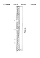
FIG. 1 is a top view of a substrate supporting a plurality of metal plates;
FIG. 2 is a sectional side view of FIG. 1 taken along line 2--2, further showing an insulating layer and mask layer over the substrate and, metal plates;
FIGS. 3a-3b are views similar to those of FIGS. 1 and 2, respectively, further showing vias in the mask and insulating layer;
FIG. 4 is a view similar to that of FIG. 3b, further showing a metal sheet over the mask;
FIGS. 5a-5b are views similar to those of FIGS. 3a and 4, respectively, further showing the metal sheet after patterning has formed a sacrificial layer and a portion of a coil;
FIG. 6 is a view similar to that of FIG. 5b, further showing the application of metal bridge material over the sacrificial layer and coil;
FIGS. 7a-7b are views similar to those of FIGS. 5a and 6 respectively, further showing the metal bridge remaining after the patterning of the metal bridge material;
FIG. 8 is a view similar to that of FIG. 7b, further showing a reinforcing seal layer over the metal bridge;
FIG. 9 is a view similar to that of FIG. 8, further showing a well in the reinforcing seal layer and an air gap below a portion of the metal bridge existing after the removal of the sacrificial layer; and
FIGS. 10a-10b are views similar to those of FIGS. 7a and 9, respectively, further showing a magnet in the well of the reinforcing seal layer.
FIG. 1 is a top view of a substrate 10 supporting a plurality of metal plates shown as switch contact plate 11, stationary contact plate 12, and coil contact plates 13 and 14. The number and positions of the metal plates and the plate designations are for example only.
FIG. 2 is a sectional side view of FIG. 1 taken along line 2--2, further showing an insulating layer 16 and a mask layer 17 over the substrate and metal plates. The insulating layer is a dielectric material and preferably comprises a polyimide such as Kapton polyimide (Kapton is a trademark of E. I. dupont de Nemours & Co.) having a thickness of approximately 2 mil, for example, and coated with an adhesive (not shown) such as Ultem® polyetherimide (Ultem is a trademark of General Electric Co.).
In one embodiment for fabricating mask 17, a thin seed layer 17a of titanium (about 1000 Å) is sputtered over the insulating layer, and a thicker layer 17b of copper (about 3000 Å) is formed by sputtering a thin layer of copper over the thin layer of titanium and electroplating a 4 μm layer of copper over the thin layer of copper.
FIGS. 3a-3b are views similar to those of FIGS. 1 and 2, respectively, further showing vias 18 in the metal mask and insulating layer (for simplicity, although locations of vias 18 are shown, mask 17 and insulating layer 16 are not shown in FIG. 3a). The vias can be formed in any conventional manner. Using a photoresist mask (not shown), openings having dimensions of 3 mils by 5 mils can be etched (using a ferric chloride solution for the copper and a hydrofluoric acid solution for the titanium) into the metal mask. Then an excimer laser can ablate the insulating layer through the mask to form vias 18. Mask 17, which in this embodiment remains on the insulating layer during further processing and, for the reasons discussed below, is used in a preferred embodiment, is not a necessary feature of the present invention. Other methods of forming vias in insulating layer 16 can be used, if desired.
At least one via is preferably formed on each plate. In the embodiment of FIG. 3a, the respective vias on coil contact plates 13 and 14 are used for coupling a coil to the coil contact plates, the vias on stationary contact plate 12 are used for stationary contacts, and the vias on switch contact plate 11 are used for movable contacts, as discussed below.
FIG. 4 is a view similar to that of FIG. 3b, further showing a sacrificial metal sheet 19 applied conformally over mask 17 and vias 18. Sacrificial metal sheet 19 can include sputtered and electroplated copper having a thickness of about eight microns, for example. One advantage of using metal mask 17 over insulating layer 16 and leaving the mask in place when applying sacrificial metal sheet 19 is that a portion of mask 17 can be a bottom portion of a sacrificial layer 20 (shown in FIG. 5b). This process results in a greater thickness between the insulating layer and a bridge 22 than between metal plate 11 and a moving contact 24 of bridge 22 (bridge 22 and contact 24 shown in FIG. 9).
FIGS. 5a-5b are views similar to those of FIGS. 3a and 4, respectively, further showing sacrificial metal sheet 19 and metal layer 17b after patterning has formed a sacrificial layer 20 (including a sacrificial portion of metal layer 17b) and a portion of an integral coil 20a (for simplicity, thin metal layer 17a and insulating layer 16 are not shown in FIG. 5a). In alternative embodiments either no mask 17 is present so the sacrificial metal sheet is the only portion of the sacrificial layer or the entire mask can be a sacrificial portion of the sacrificial layer which is removed during switch fabrication.
Sacrificial layer and coil patterning can be performed using a standard photoresist etch process, for example. Coil 20a, which typically has many more turns (such as about 50) than are shown in FIG. 5a, is formed so that one end extends through a via 18 on coil contact plate 13 and the other end extends through a via 18 on coil contact plate 14. Sacrificial layer 20 extends over the vias on switch contact plate 11 and can extend onto stationary contact plate 12, but preferably does not extend over the vias of stationary contact plate 12.
In the embodiment shown in FIG. 5b, only the copper layers 19 and 17b are etched; the thin metal layer 17a of titanium remains on insulating layer 16 and can thus be used for adhesion of the remainder of a metal bridge, as discussed below.
FIG. 6 is a view similar to that of FIG. 5b, further showing the application of metal bridge material 22 over sacrificial layer 20 and coil 20a. In one embodiment, the metal bridge material includes a first layer 22a of sputtered gold having a thickness of about 1000 Å and electroplated gold having a thickness of about 10 μm and a second layer 22b of sputtered titanium having a thickness of about 1 μm. A moving contact portion 24 of the metal bridge material represents a contact of the metal bridge which will be movable after completion of the switch, and a stationary contact portion 26 of the metal bridge represents a contact of the bridge which has a fixed position in direct contact with stationary contact plate 12.
FIGS. 7a-7b are views similar to those of FIGS. 5a and 6 respectively, further showing the metal bridge 22 remaining after patterning of the metal bridge material (for simplicity, insulating layer 16 is not shown in FIG. 7a). Using a photoresist mask, the top layer of titanium 22b can be selectively etched, followed by the gold layer 22a, and the titanium layer 17a. During the patterning, openings 30 are formed in the metal bridge over selected portions of sacrificial layer 20, and coil 20a is completed. The switch can be designed in any desired manner. In the embodiment of FIG. 7a, portions of bridge 22 serve as anchors 28 for supporting the bridge.
FIG. 8 is a view similar to that of FIG. 7b, further showing a reinforcing seal layer 32 over the metal bridge. The seal layer comprises a nonconductive, flexible material such as Kapton polyimide, for example. In a preferred embodiment, the Kapton polyimide is coated with SPl(silicon polyimide)/epoxy for adhesion to the bridge. Preferably seal layer 32 also extends over coil 20a to protect the coil from becoming etched during later etch steps.
FIG. 9 is a view similar to that of FIG. 8, further showing a well 40 in reinforcing seal layer 32 and an air gap 34 below a portion of the metal bridge existing after removal of the sacrificial layer. The well can be formed in seal layer 32 in a similar manner as vias 18 are formed in insulating layer 16, as discussed with respect to FIG. 3b. If a mask (not shown) is used for forming well 40, the mask is then removed.
After sacrificial layer 20 is removed, bridge 22, with moving contact 24, forms flexible hinges 29 and thus provides a spring-like contact with switch contact plate 11. Seal layer 32 also serves as part of the flexible hinges.
FIGS. 10a-10b are views similar to those of FIGS. 7a and 9, respectively, further showing an attached magnet 36 in well 40 of seal layer 32 (for simplicity, insulating layer 16 and seal layer 32 are not shown in FIG. 10a). Preferably magnet 36 is a rare earth permanent magnet such as NdFeB. Adhesive (not shown), such as either Ultem polyetherimide or Torlon polyamideimide (Torlon is a trademark of Amoco Performance Products Inc., of Greenville, S.C.), can be applied to the bottom of the magnet before placement, or the magnet and switch can be spray coated with adhesive after placement of the magnet.
The seal layer forms a flexible reinforcement to the metal hinges 29 of the bridge and prevents particles from interfering with the bridge during dicing of switches and when the switch is used.
While only certain preferred features of the invention have been illustrated and described herein, many modifications and changes will occur to those skilled in the art. It is, therefore, to be understood that the appended claims are intended to cover all such modifications and changes as fall within the true spirit of the invention.
Claims (6)
1. A micromachined switch, comprising:
a metal plate;
an insulating layer over said metal plate, said insulating layer having at least one via extending to said metal plate;
a metal bridge situated above said at least one via and having a switch contact extending into a portion of said at least one via, said metal bridge and said insulating layer having an air gap therebetween with said metal bridge having at least one opening adjacent said air gap;
an electrically conductive coil situated on said insulating layer and surrounding at least a portion of said metal bridge; and
a reinforcing seal layer over said metal bridge and said coil.
2. The switch of claim 1, wherein said reinforcing seal layer has a well situated adjacent to a portion of said metal bridge including at least a portion of said at least one opening, and further including a magnet situated in said well of said seal layer.
3. The switch of claim 1, wherein said insulating layer and said seal layer are each comprised of polyimide material.
4. The switch of claim 3, wherein at least a top portion of said metal plate and at least a bottom portion of said metal bridge comprise gold.
5. The switch of claim 1, further including an additional metal plate, wherein said insulating layer is further situated over said additional metal plate and has at least one additional via extending to said additional metal plate.
6. The switch of claim 5, wherein said metal bridge extends directly into said at least one additional via so as to make contact with said additional metal plate.
Priority Applications (1)
| Application Number | Priority Date | Filing Date | Title |
|---|---|---|---|
| US08/626,311 US5652559A (en) | 1993-12-20 | 1996-04-01 | Method of micromachining electromagnetically actuated current switches with polyimide reinforcement seals, and switches produced thereby |
Applications Claiming Priority (2)
| Application Number | Priority Date | Filing Date | Title |
|---|---|---|---|
| US08/169,272 US5531018A (en) | 1993-12-20 | 1993-12-20 | Method of micromachining electromagnetically actuated current switches with polyimide reinforcement seals, and switches produced thereby |
| US08/626,311 US5652559A (en) | 1993-12-20 | 1996-04-01 | Method of micromachining electromagnetically actuated current switches with polyimide reinforcement seals, and switches produced thereby |
Related Parent Applications (1)
| Application Number | Title | Priority Date | Filing Date |
|---|---|---|---|
| US08/169,272 Division US5531018A (en) | 1993-12-20 | 1993-12-20 | Method of micromachining electromagnetically actuated current switches with polyimide reinforcement seals, and switches produced thereby |
Publications (1)
| Publication Number | Publication Date |
|---|---|
| US5652559A true US5652559A (en) | 1997-07-29 |
Family
ID=22614946
Family Applications (2)
| Application Number | Title | Priority Date | Filing Date |
|---|---|---|---|
| US08/169,272 Expired - Lifetime US5531018A (en) | 1993-12-20 | 1993-12-20 | Method of micromachining electromagnetically actuated current switches with polyimide reinforcement seals, and switches produced thereby |
| US08/626,311 Expired - Lifetime US5652559A (en) | 1993-12-20 | 1996-04-01 | Method of micromachining electromagnetically actuated current switches with polyimide reinforcement seals, and switches produced thereby |
Family Applications Before (1)
| Application Number | Title | Priority Date | Filing Date |
|---|---|---|---|
| US08/169,272 Expired - Lifetime US5531018A (en) | 1993-12-20 | 1993-12-20 | Method of micromachining electromagnetically actuated current switches with polyimide reinforcement seals, and switches produced thereby |
Country Status (1)
| Country | Link |
|---|---|
| US (2) | US5531018A (en) |
Cited By (16)
| Publication number | Priority date | Publication date | Assignee | Title |
|---|---|---|---|---|
| US5945203A (en) * | 1997-10-14 | 1999-08-31 | Zms Llc | Stratified composite dielectric and method of fabrication |
| US5989989A (en) * | 1996-05-31 | 1999-11-23 | Texas Instruments Incorporated | Die and cube reroute process |
| US5994986A (en) * | 1997-02-27 | 1999-11-30 | Nec Corporation | High frequency relay |
| WO2001035484A1 (en) * | 1999-11-12 | 2001-05-17 | The Trustees Of The University Of Pennsylvania | Minute electromechanical actuation and fluid control devices and integrated systems based on low temperature co-fired ceramic (ltcc) tape technology |
| US6423566B1 (en) * | 1998-07-24 | 2002-07-23 | International Business Machines Corporation | Moisture and ion barrier for protection of devices and interconnect structures |
| WO2002064495A2 (en) * | 2001-02-12 | 2002-08-22 | International Business Machines Corporation | Enhanced sacrificial layer etching technique for microstructure release |
| US20020121145A1 (en) * | 2000-05-16 | 2002-09-05 | Deconde Keith D. | Fingerprint sensors using membrane switch arrays |
| US6458618B1 (en) | 1998-06-05 | 2002-10-01 | Georgia Tech Research Corporation | Robust substrate-based micromachining techniques and their application to micromachined sensors and actuators |
| WO2002096796A2 (en) * | 2001-05-25 | 2002-12-05 | Raytheon Company | Membrane for micro-electro-mechanical switch, and methods of making and using it |
| US6509623B2 (en) * | 2000-06-15 | 2003-01-21 | Newport Fab, Llc | Microelectronic air-gap structures and methods of forming the same |
| US6791441B2 (en) | 2002-05-07 | 2004-09-14 | Raytheon Company | Micro-electro-mechanical switch, and methods of making and using it |
| US20050223818A1 (en) * | 2000-05-16 | 2005-10-13 | Deconde Keith T | Method and apparatus for protection of contour sensing devices |
| US8033838B2 (en) | 1996-02-21 | 2011-10-11 | Formfactor, Inc. | Microelectronic contact structure |
| US20130032453A1 (en) * | 2011-08-03 | 2013-02-07 | Cavendish Kinetics Inc. | Elimination of silicon residues from mems cavity floor |
| US8373428B2 (en) | 1993-11-16 | 2013-02-12 | Formfactor, Inc. | Probe card assembly and kit, and methods of making same |
| EP2761640A2 (en) * | 2011-09-30 | 2014-08-06 | Telepath Networks, Inc. | Multi integrated switching device structures |
Families Citing this family (47)
| Publication number | Priority date | Publication date | Assignee | Title |
|---|---|---|---|---|
| US5698112A (en) * | 1994-11-24 | 1997-12-16 | Siemens Aktiengesellschaft | Corrosion protection for micromechanical metal layers |
| US5847631A (en) * | 1995-10-10 | 1998-12-08 | Georgia Tech Research Corporation | Magnetic relay system and method capable of microfabrication production |
| DE19716480B4 (en) * | 1997-04-19 | 2004-03-25 | Micronas Semiconductor Holding Ag | Method for producing a device with a cavity for receiving an optical waveguide |
| CH692829A5 (en) * | 1997-11-20 | 2002-11-15 | Axicom Ltd | Microrelay as miniaturized flat coil relay. |
| EP0996157B1 (en) * | 1998-10-21 | 2005-08-03 | STMicroelectronics S.r.l. | Process for manufacturing integrated devices comprising microstructures and associated suspended electrical interconnections |
| US6396368B1 (en) | 1999-11-10 | 2002-05-28 | Hrl Laboratories, Llc | CMOS-compatible MEM switches and method of making |
| US6426722B1 (en) | 2000-03-08 | 2002-07-30 | Hrl Laboratories, Llc | Polarization converting radio frequency reflecting surface |
| US6812903B1 (en) | 2000-03-14 | 2004-11-02 | Hrl Laboratories, Llc | Radio frequency aperture |
| US6518931B1 (en) | 2000-03-15 | 2003-02-11 | Hrl Laboratories, Llc | Vivaldi cloverleaf antenna |
| US6538621B1 (en) | 2000-03-29 | 2003-03-25 | Hrl Laboratories, Llc | Tunable impedance surface |
| US6552696B1 (en) | 2000-03-29 | 2003-04-22 | Hrl Laboratories, Llc | Electronically tunable reflector |
| US6496155B1 (en) | 2000-03-29 | 2002-12-17 | Hrl Laboratories, Llc. | End-fire antenna or array on surface with tunable impedance |
| US6483480B1 (en) | 2000-03-29 | 2002-11-19 | Hrl Laboratories, Llc | Tunable impedance surface |
| US7217977B2 (en) | 2004-04-19 | 2007-05-15 | Hrl Laboratories, Llc | Covert transformation of transistor properties as a circuit protection method |
| US6815816B1 (en) * | 2000-10-25 | 2004-11-09 | Hrl Laboratories, Llc | Implanted hidden interconnections in a semiconductor device for preventing reverse engineering |
| US6483481B1 (en) | 2000-11-14 | 2002-11-19 | Hrl Laboratories, Llc | Textured surface having high electromagnetic impedance in multiple frequency bands |
| US6791191B2 (en) | 2001-01-24 | 2004-09-14 | Hrl Laboratories, Llc | Integrated circuits protected against reverse engineering and method for fabricating the same using vias without metal terminations |
| US7294935B2 (en) * | 2001-01-24 | 2007-11-13 | Hrl Laboratories, Llc | Integrated circuits protected against reverse engineering and method for fabricating the same using an apparent metal contact line terminating on field oxide |
| US6774413B2 (en) | 2001-06-15 | 2004-08-10 | Hrl Laboratories, Llc | Integrated circuit structure with programmable connector/isolator |
| US6740942B2 (en) * | 2001-06-15 | 2004-05-25 | Hrl Laboratories, Llc. | Permanently on transistor implemented using a double polysilicon layer CMOS process with buried contact |
| US6739028B2 (en) * | 2001-07-13 | 2004-05-25 | Hrl Laboratories, Llc | Molded high impedance surface and a method of making same |
| US6670921B2 (en) | 2001-07-13 | 2003-12-30 | Hrl Laboratories, Llc | Low-cost HDMI-D packaging technique for integrating an efficient reconfigurable antenna array with RF MEMS switches and a high impedance surface |
| US6545647B1 (en) | 2001-07-13 | 2003-04-08 | Hrl Laboratories, Llc | Antenna system for communicating simultaneously with a satellite and a terrestrial system |
| US6897535B2 (en) * | 2002-05-14 | 2005-05-24 | Hrl Laboratories, Llc | Integrated circuit with reverse engineering protection |
| US7276990B2 (en) * | 2002-05-15 | 2007-10-02 | Hrl Laboratories, Llc | Single-pole multi-throw switch having low parasitic reactance, and an antenna incorporating the same |
| US7298228B2 (en) * | 2002-05-15 | 2007-11-20 | Hrl Laboratories, Llc | Single-pole multi-throw switch having low parasitic reactance, and an antenna incorporating the same |
| US7049667B2 (en) * | 2002-09-27 | 2006-05-23 | Hrl Laboratories, Llc | Conductive channel pseudo block process and circuit to inhibit reverse engineering |
| US6979606B2 (en) | 2002-11-22 | 2005-12-27 | Hrl Laboratories, Llc | Use of silicon block process step to camouflage a false transistor |
| WO2004055868A2 (en) * | 2002-12-13 | 2004-07-01 | Hrl Laboratories, Llc | Integrated circuit modification using well implants |
| US7164387B2 (en) * | 2003-05-12 | 2007-01-16 | Hrl Laboratories, Llc | Compact tunable antenna |
| US7456803B1 (en) | 2003-05-12 | 2008-11-25 | Hrl Laboratories, Llc | Large aperture rectenna based on planar lens structures |
| US7071888B2 (en) * | 2003-05-12 | 2006-07-04 | Hrl Laboratories, Llc | Steerable leaky wave antenna capable of both forward and backward radiation |
| US7068234B2 (en) * | 2003-05-12 | 2006-06-27 | Hrl Laboratories, Llc | Meta-element antenna and array |
| US7253699B2 (en) * | 2003-05-12 | 2007-08-07 | Hrl Laboratories, Llc | RF MEMS switch with integrated impedance matching structure |
| US7245269B2 (en) * | 2003-05-12 | 2007-07-17 | Hrl Laboratories, Llc | Adaptive beam forming antenna system using a tunable impedance surface |
| US7154451B1 (en) | 2004-09-17 | 2006-12-26 | Hrl Laboratories, Llc | Large aperture rectenna based on planar lens structures |
| US20070211403A1 (en) * | 2003-12-05 | 2007-09-13 | Hrl Laboratories, Llc | Molded high impedance surface |
| US7242063B1 (en) | 2004-06-29 | 2007-07-10 | Hrl Laboratories, Llc | Symmetric non-intrusive and covert technique to render a transistor permanently non-operable |
| JP4907544B2 (en) * | 2004-10-27 | 2012-03-28 | エプコス アクチエンゲゼルシャフト | Electronic devices |
| US7307589B1 (en) | 2005-12-29 | 2007-12-11 | Hrl Laboratories, Llc | Large-scale adaptive surface sensor arrays |
| US8168487B2 (en) | 2006-09-28 | 2012-05-01 | Hrl Laboratories, Llc | Programmable connection and isolation of active regions in an integrated circuit using ambiguous features to confuse a reverse engineer |
| US8212739B2 (en) | 2007-05-15 | 2012-07-03 | Hrl Laboratories, Llc | Multiband tunable impedance surface |
| US7868829B1 (en) | 2008-03-21 | 2011-01-11 | Hrl Laboratories, Llc | Reflectarray |
| US8436785B1 (en) | 2010-11-03 | 2013-05-07 | Hrl Laboratories, Llc | Electrically tunable surface impedance structure with suppressed backward wave |
| US9466887B2 (en) | 2010-11-03 | 2016-10-11 | Hrl Laboratories, Llc | Low cost, 2D, electronically-steerable, artificial-impedance-surface antenna |
| US8994609B2 (en) | 2011-09-23 | 2015-03-31 | Hrl Laboratories, Llc | Conformal surface wave feed |
| US8982011B1 (en) | 2011-09-23 | 2015-03-17 | Hrl Laboratories, Llc | Conformal antennas for mitigation of structural blockage |
Citations (4)
| Publication number | Priority date | Publication date | Assignee | Title |
|---|---|---|---|---|
| US5262000A (en) * | 1989-09-26 | 1993-11-16 | British Telecommunications Public Limited Company | Method for making micromechanical switch |
| US5374792A (en) * | 1993-01-04 | 1994-12-20 | General Electric Company | Micromechanical moving structures including multiple contact switching system |
| US5384483A (en) * | 1992-02-28 | 1995-01-24 | Sgs-Thomson Microelectronics, Inc. | Planarizing glass layer spaced from via holes |
| US5472539A (en) * | 1994-06-06 | 1995-12-05 | General Electric Company | Methods for forming and positioning moldable permanent magnets on electromagnetically actuated microfabricated components |
-
1993
- 1993-12-20 US US08/169,272 patent/US5531018A/en not_active Expired - Lifetime
-
1996
- 1996-04-01 US US08/626,311 patent/US5652559A/en not_active Expired - Lifetime
Patent Citations (4)
| Publication number | Priority date | Publication date | Assignee | Title |
|---|---|---|---|---|
| US5262000A (en) * | 1989-09-26 | 1993-11-16 | British Telecommunications Public Limited Company | Method for making micromechanical switch |
| US5384483A (en) * | 1992-02-28 | 1995-01-24 | Sgs-Thomson Microelectronics, Inc. | Planarizing glass layer spaced from via holes |
| US5374792A (en) * | 1993-01-04 | 1994-12-20 | General Electric Company | Micromechanical moving structures including multiple contact switching system |
| US5472539A (en) * | 1994-06-06 | 1995-12-05 | General Electric Company | Methods for forming and positioning moldable permanent magnets on electromagnetically actuated microfabricated components |
Cited By (35)
| Publication number | Priority date | Publication date | Assignee | Title |
|---|---|---|---|---|
| US8373428B2 (en) | 1993-11-16 | 2013-02-12 | Formfactor, Inc. | Probe card assembly and kit, and methods of making same |
| US8033838B2 (en) | 1996-02-21 | 2011-10-11 | Formfactor, Inc. | Microelectronic contact structure |
| US5989989A (en) * | 1996-05-31 | 1999-11-23 | Texas Instruments Incorporated | Die and cube reroute process |
| US5994986A (en) * | 1997-02-27 | 1999-11-30 | Nec Corporation | High frequency relay |
| US5945203A (en) * | 1997-10-14 | 1999-08-31 | Zms Llc | Stratified composite dielectric and method of fabrication |
| US6458618B1 (en) | 1998-06-05 | 2002-10-01 | Georgia Tech Research Corporation | Robust substrate-based micromachining techniques and their application to micromachined sensors and actuators |
| US6423566B1 (en) * | 1998-07-24 | 2002-07-23 | International Business Machines Corporation | Moisture and ion barrier for protection of devices and interconnect structures |
| WO2001035484A1 (en) * | 1999-11-12 | 2001-05-17 | The Trustees Of The University Of Pennsylvania | Minute electromechanical actuation and fluid control devices and integrated systems based on low temperature co-fired ceramic (ltcc) tape technology |
| US6889565B2 (en) | 2000-05-16 | 2005-05-10 | Fidelica Microsystems, Inc. | Fingerprint sensors using membrane switch arrays |
| US20050229380A1 (en) * | 2000-05-16 | 2005-10-20 | Deconde Keith T | Fingerprint sensors using membrane switch arrays |
| US7437953B2 (en) | 2000-05-16 | 2008-10-21 | Deconde Keith T | Method and apparatus for protection of contour sensing devices |
| US7316167B2 (en) | 2000-05-16 | 2008-01-08 | Fidelica, Microsystems, Inc. | Method and apparatus for protection of contour sensing devices |
| US6578436B1 (en) | 2000-05-16 | 2003-06-17 | Fidelica Microsystems, Inc. | Method and apparatus for pressure sensing |
| US20070289392A1 (en) * | 2000-05-16 | 2007-12-20 | Fidelica Microsystems, Inc. | Method and apparatus for protection of contour sensing devices |
| US20020121145A1 (en) * | 2000-05-16 | 2002-09-05 | Deconde Keith D. | Fingerprint sensors using membrane switch arrays |
| US7638350B2 (en) | 2000-05-16 | 2009-12-29 | Springworks Llc | Fingerprint sensors using membrane switch arrays |
| US20050223818A1 (en) * | 2000-05-16 | 2005-10-13 | Deconde Keith T | Method and apparatus for protection of contour sensing devices |
| US6509623B2 (en) * | 2000-06-15 | 2003-01-21 | Newport Fab, Llc | Microelectronic air-gap structures and methods of forming the same |
| WO2002064495A2 (en) * | 2001-02-12 | 2002-08-22 | International Business Machines Corporation | Enhanced sacrificial layer etching technique for microstructure release |
| WO2002064495A3 (en) * | 2001-02-12 | 2003-06-05 | Ibm | Enhanced sacrificial layer etching technique for microstructure release |
| WO2002096796A2 (en) * | 2001-05-25 | 2002-12-05 | Raytheon Company | Membrane for micro-electro-mechanical switch, and methods of making and using it |
| US6803534B1 (en) | 2001-05-25 | 2004-10-12 | Raytheon Company | Membrane for micro-electro-mechanical switch, and methods of making and using it |
| WO2002096796A3 (en) * | 2001-05-25 | 2003-03-13 | Raytheon Co | Membrane for micro-electro-mechanical switch, and methods of making and using it |
| US20050012577A1 (en) * | 2002-05-07 | 2005-01-20 | Raytheon Company, A Delaware Corporation | Micro-electro-mechanical switch, and methods of making and using it |
| US7002441B2 (en) | 2002-05-07 | 2006-02-21 | Raytheon Company | Micro-electro-mechanical switch, and methods of making and using it |
| US6791441B2 (en) | 2002-05-07 | 2004-09-14 | Raytheon Company | Micro-electro-mechanical switch, and methods of making and using it |
| US20130032453A1 (en) * | 2011-08-03 | 2013-02-07 | Cavendish Kinetics Inc. | Elimination of silicon residues from mems cavity floor |
| WO2013020039A3 (en) * | 2011-08-03 | 2013-03-21 | Cavendish Kinetics, Inc | Elimination of silicon residues from mems cavity floor |
| CN103732528A (en) * | 2011-08-03 | 2014-04-16 | 卡文迪什动力有限公司 | Elimination of silicon residues from MEMS cavity floor |
| JP2014521527A (en) * | 2011-08-03 | 2014-08-28 | キャベンディッシュ・キネティックス・インコーポレイテッド | Elimination of silicon residue from the bottom of the MEMS cavity |
| US8921165B2 (en) * | 2011-08-03 | 2014-12-30 | Cavendish Kinetics, Inc. | Elimination of silicon residues from MEMS cavity floor |
| CN103732528B (en) * | 2011-08-03 | 2018-09-28 | 卡文迪什动力有限公司 | Silicon residue is eliminated from MEMS cavity bottoms |
| EP2761640A2 (en) * | 2011-09-30 | 2014-08-06 | Telepath Networks, Inc. | Multi integrated switching device structures |
| EP2761640A4 (en) * | 2011-09-30 | 2015-04-29 | Telepath Networks Inc | Multi integrated switching device structures |
| US9324526B2 (en) | 2011-09-30 | 2016-04-26 | Telepath Networks, Inc. | Multi integrated switching device structures |
Also Published As
| Publication number | Publication date |
|---|---|
| US5531018A (en) | 1996-07-02 |
Similar Documents
| Publication | Publication Date | Title |
|---|---|---|
| US5652559A (en) | Method of micromachining electromagnetically actuated current switches with polyimide reinforcement seals, and switches produced thereby | |
| US5454904A (en) | Micromachining methods for making micromechanical moving structures including multiple contact switching system | |
| US7202764B2 (en) | Noble metal contacts for micro-electromechanical switches | |
| JP4205202B2 (en) | Magnetic microswitch and manufacturing method thereof | |
| US6440767B1 (en) | Monolithic single pole double throw RF MEMS switch | |
| US6778046B2 (en) | Latching micro magnetic relay packages and methods of packaging | |
| US7242066B2 (en) | Manufacturing method of a microelectromechanical switch | |
| US7233048B2 (en) | MEMS device trench plating process and apparatus for through hole vias | |
| US8238074B2 (en) | Capacitive RF-MEMS device with integrated decoupling capacitor | |
| US20080079120A1 (en) | Interconnect structure using through wafer vias and method of fabrication | |
| EP0879471A2 (en) | Bulk fabricated electromagnetic micro-relays/micro-switches and method of making same | |
| EP1672661A2 (en) | MEMS switch and method of fabricating the same | |
| KR100691046B1 (en) | Electrode patterning for a differential pzt activator | |
| EP1642311A2 (en) | Micro-electromechanical device and module and method of manufacturing same | |
| EP0635821A1 (en) | A process for the fabrication of thin film magnetic heads | |
| US7965159B2 (en) | Micro-switching device and manufacturing method for the same | |
| US7816999B2 (en) | Single-pole double-throw MEMS switch | |
| EP1556877B1 (en) | A micromachined relay with inorganic insulation | |
| US8343791B2 (en) | Plating process and apparatus for through wafer features | |
| JP2751242B2 (en) | Method for manufacturing semiconductor device | |
| CN101194333A (en) | Single-pole double-throw MEMS switch | |
| JPS63124552A (en) | Manufacture of semiconductor device | |
| JP2003242850A (en) | Contact for electrical switch and its manufacturing method as well as electrical switch | |
| JP2778879B2 (en) | Forming method of small drive mechanism | |
| KR100492531B1 (en) | Field emission device and manufacturing method thereof |
Legal Events
| Date | Code | Title | Description |
|---|---|---|---|
| FEPP | Fee payment procedure |
Free format text: PAYOR NUMBER ASSIGNED (ORIGINAL EVENT CODE: ASPN); ENTITY STATUS OF PATENT OWNER: LARGE ENTITY |
|
| STCF | Information on status: patent grant |
Free format text: PATENTED CASE |
|
| REMI | Maintenance fee reminder mailed | ||
| FPAY | Fee payment |
Year of fee payment: 4 |
|
| SULP | Surcharge for late payment | ||
| REMI | Maintenance fee reminder mailed | ||
| FPAY | Fee payment |
Year of fee payment: 8 |
|
| SULP | Surcharge for late payment |
Year of fee payment: 7 |
|
| FPAY | Fee payment |
Year of fee payment: 12 |