US5597332A - Solder contact - Google Patents
Solder contact Download PDFInfo
- Publication number
- US5597332A US5597332A US08/286,704 US28670494A US5597332A US 5597332 A US5597332 A US 5597332A US 28670494 A US28670494 A US 28670494A US 5597332 A US5597332 A US 5597332A
- Authority
- US
- United States
- Prior art keywords
- contact
- housing
- spring arm
- spring arms
- arm support
- Prior art date
- Legal status (The legal status is an assumption and is not a legal conclusion. Google has not performed a legal analysis and makes no representation as to the accuracy of the status listed.)
- Expired - Fee Related
Links
Images


Classifications
-
- H—ELECTRICITY
- H01—ELECTRIC ELEMENTS
- H01R—ELECTRICALLY-CONDUCTIVE CONNECTIONS; STRUCTURAL ASSOCIATIONS OF A PLURALITY OF MUTUALLY-INSULATED ELECTRICAL CONNECTING ELEMENTS; COUPLING DEVICES; CURRENT COLLECTORS
- H01R12/00—Structural associations of a plurality of mutually-insulated electrical connecting elements, specially adapted for printed circuits, e.g. printed circuit boards [PCB], flat or ribbon cables, or like generally planar structures, e.g. terminal strips, terminal blocks; Coupling devices specially adapted for printed circuits, flat or ribbon cables, or like generally planar structures; Terminals specially adapted for contact with, or insertion into, printed circuits, flat or ribbon cables, or like generally planar structures
- H01R12/50—Fixed connections
- H01R12/51—Fixed connections for rigid printed circuits or like structures
- H01R12/55—Fixed connections for rigid printed circuits or like structures characterised by the terminals
- H01R12/58—Fixed connections for rigid printed circuits or like structures characterised by the terminals terminals for insertion into holes
Definitions
- the invention concerns a single piece solder contact made of a punched piece of metal.
- solder contact is known from German Patent No. 4,103,423 C2.
- the contact position is arranged in this contact so that it is continually mobile, so that relative movements between the contact pin and the contact position of the solder contact can be prevented, while the contact position is especially movable in the plug axis direction and perpendicular to it, and thus it can follow the movements of a contact pin or the solder contact soldered to a printed-circuit board assembly.
- solder contact is of relatively large volume on account of the special swingable mounting.
- a similar solder contact is known from German Patent No. 4,109,519 A1; it has a basically cuboid form, with the contact areas provided perpendicularly centered at two opposite side surfaces; [these contact areas] are respectively connected to the front edges of the cuboid contact via meandering strips.
- the contact position is arranged at the center of the cuboid solder contact and is provided with a fixed elasticity in the direction of the side walls.
- the path of a contact pin inserted into such a solder contact is thus limited by the front edges of the solder contact and they both are movable through the contact areas that have the meandering strips, each independently of the other, so that there is no contact position here with an exactly defined distance.
- the problem of the invention is to create a solder contact with small space requirements, which has a movable contact position.
- a relatively long bow spring arm support can be provided in a small housing, so that the desired mobility of the contact position is achieved, which makes it possible for a contact pin that is plugged into a contact position to move independently of the housing of the solder contact.
- a release of the solder contact of a housing soldered to a printed-circuit board due to vibrations of a contact pin that is plugged into the contact position is eliminated, when only small movement forces are transferred by the contact pin through the contact position to the housing of the solder contact soldered onto a printed-circuit board.
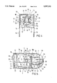
- FIG. 1 a side view of an embodiment of a solder contact according to the invention with the side wall cut away;
- FIG. 2 a side view of the solder contact from FIG. 1;
- FIG. 3 a plan view of the solder contact from FIG. 1;
- FIG. 4 a front view of the solder contact from FIG. 1;
- FIG. 5 a bottom view of the solder contact from FIG. 1;
- FIG. 6 a side view of a second embodiment of the solder contact according to the invention with the side wall cut away;
- FIG. 7 a side view of the solder contact from FIG. 6;
- FIG. 8 a side view of a third embodiment of a solder contact according to the invention.
- FIG. 9 a plan view of the solder contact from FIG. 9;
- FIG. 10 a bottom view of the solder contact from FIG. 8;
- FIG. 11 spring arm forming a contact position, in cross-section along line A--A of FIG. 10;
- FIG. 12 a front view of the solder contact from FIG. 8 showing the side of the solder contact to which the bow spring arm support is connected;
- FIG. 13 a front side of the solder contact from FIG. 8, which shows the side of the contact position of the solder contact.
- a first embodiment of a solder contact according to the invention comprises two side walls 1 and 2 as well as a covering wall 3 (FIGS. 1-5).
- the side walls 1 and 2 are at right angles to the covering wall 3, so that a housing of a type that is open from below and has a U-shaped cross section is formed.
- the covering wall 3 exhibits a free back edge 4, which proceeds linearly, and a free leading edge 5, which proceeds as a semicircle.
- a bead 6 running parallel to the back edge 4 is pressed into the covering wall 3, and extends over the side walls 1 and 2, so that the U shape of the housing is kept from widening by the bead 6.
- a plug hole 7, which is about 1.5 mm in diameter is punched out in the covering wall 3 so that a plug contact pin (not illustrated) of about 1 mm thickness can be passed through.
- a catch tab 8 can be passed through a U-shaped free punch 9 indicating the hole 7; it is folded at a right angle toward the inside of the housing.
- the side walls 1,2 exhibit free linear back edges 10,11, linear leading edges 12,13, as well as free linear lower edges 14,15.
- a soldering post 16 is connected that extends from the edge; moreover, it is a short distance from the back edge 10 or 11.
- a short distance from each soldering post 16, an overhanging support tab 17 for supporting the housing is connected to a printed-circuit board 17a, whose function will be explained further below.
- Each side wall 1,2 can exhibit a bead 18 running parallel to the back edges 10,11 in the area between the soldering post 16 and the leading edge 12 or 13 in order to brace it; this extends in each case somewhat into the covering wall 3.
- holes 19,19a are punched out at the longitudinal edges 20 in the transfer area between the side walls 1,2 and the covering wall 3, and suitably in the area between the beads 6 and 18, as well as between the bead 18 and the front edge 12 or 13.
- the side wall 2 exhibits an additional catch tab 21, which is formed from an indentation built in running parallel to the lower edge 15 at a distance from it, running from the leading edge 13 to here, whereby the catch tab 21 is turned at a right angle in the housing in such a way that it finds its free longitudinal edge 21a, which points toward the covering wall 3, at a distance under the free longitudinal edge 8a of the catch tab 8.
- catch tabs 8,21 The function of the catch tabs 8,21 is explained further below.
- a support bead 22 passes through the bending and is pressed into the longitudinal extension of the tab; in addition, it exhibits further lateral support tabs 17 for supporting the catch tabs 21 on the printed-circuit board 17a.
- the catch tabs 8 and 21 are set very close to each other, whereby the catch tabs 8 are closer to the back edges 10,11 and the catch tabs 21 come to lie close to the leading edges 12,13.
- the function of the relative load of the catch tabs 8,21 is more closely and extensively explained below.
- the side wall 1 exhibits a right-angled bow spring arm support 23, which is formed from two indentations 24 and 25 built into the back edge 10 of this side wall and runs approximately centrally between the covering wall 3 and the free lower edge 14 of the side wall 1. Issuing from its connection area at the side wall 1, the bow spring arm support 23 proceeds to bend in a semicircle, and this arched area 26 extends over the back edge 4 of the covering wall 3 slightly to the outside. At the end of the arched area 26, the bow spring arm support 23 runs parallel to the side walls 1 and 2 at a distance from them in an intersecting plane perpendicular to the ceiling wall 3 and closer to side wall 2.
- a U-shaped spring arm base 28 is attached, which exhibits a U-shaped base support 29, which bends outward to the covering wall 3, with a spring casing line proceeding in the longitudinal direction of the housing and two straight U posts 30 and 31, which proceed parallel to the side wall 1,2; these project on both sides over the longitudinal edges of the straight bow spring arm area 27, and from this area, the post 31 lies in the elongation of the straight bow spring arm area 27.
- the spring arm base 28, on account of the eccentric load of the straight bow spring arm area 27, is separated from the side walls 1,2 by the same distance, and lies with its front edge separated from the catch tabs 8,21.
- an intersecting U-shaped bead 32 is pressed in, through which the spring arm base 28 is kept from expanding.
- catch tabs 36-39 are arranged perpendicular to the longitudinal extension, bending away from the spring arms 33,34, running through indentations that are parallel to one another in the connection area of the contact spring arms 33,34 at the U posts 30,31; these tabs cooperate with the catch edges 8a and 21a.
- the spring arm catch tabs 36-39 are bent outward by 90 -- from the spring arms 33,34 and are separated by their free perpendicular edges from the catch edges 8a, 21a, so that the spring arms 33,34 extend freely throughout the narrowing that is located through the catch tabs 8 and 21, which lie opposite one another.
- the indentations that locate the catch tabs 36-39 are separated from one another in the longitudinal direction of the spring arm 33,34 in such a way that the spring arm catch tabs 36-39 also exhibit a distance from the catch tabs 8,21 in this direction.
- the catch tab 8 lies closer to the free front edges of the U posts 30,31 that are indented than does the tab 21, which, for its part, lies closer to the back edge of the contact areas 40,41 of the spring arm on the side of the contact position, positioned by the indentations, than does tab 8.
- the mobility of the bow spring arm support 23 is limited from above and below by the distance from the catch edges 8a, 21a to the catch tabs 36-39.
- the mobility of the bow spring arm support can be limited laterally by the side wall 1,2 or by a catch of the back edge of the contact sections 40,41 at the catch tab 21.
- the contact position 35 is located by the contact areas 40 and 41 of the contact spring arms 33,34, which connect to the catch tabs 36-39 and stretch over the plug hole 7.
- the contact areas 40 and 41 are bent away around the central longitudinal axis of the housing on both sides of this axis to be perpendicular toward the outside on the side walls 1,2. Through this bending, the contact areas 40,41 are braced, and additionally, they form a location funnel 42 that lies opposite the plug hole 7 and expands up to this point.
- the curved contact sections 40,41 lie perpendicular to its arched casing lines, which are parallel to the central longitudinal axis, with a minimal distance opposite this, and so form the contact position 35.
- a right-angled bow spring support 44 is connected to the front edge of the contact area 40; it is narrower than the contact area 40, it encompasses the other contact area 41 laterally from the outside with its free end 45, and with its free front edge 43, it lies in a plane that intersects the center of the plug hole.
- the section 46 with which the bow spring support 44 lies near the outer side of the contact area 41 is bent out slightly convex or partially cylindrically on the contact area 41 with arched casing lines running in the longitudinal direction and forms an abutment that presses the level of the contact position 35 outside against the contact area 41.
- the bow spring arm support 23 is likewise characterized by weak spring characteristics, which is a result of its great length and due to which it is achieved that the contact position 35 that firmly holds the contact pin is permanently movable, so that relative movements between the contact pin and the contact position are prevented, while the contact position 35, in particular, is movable in the plug axis direction, as well as perpendicular to it, so that the contact position 35 can follow the movements of the contact pin, which occur in the range of the freedom of movement of the spring arms 33,34 in the area of its catch tabs 36-39 opposite the catch tabs 8,21 fastened to the housing.
- the particular swingable mounting of the contact position 35 is reached with a small volume of the solder contact because of the long bow spring arm support 23, which, as an alternative to the projecting embodiment described, may also be lengthened due to the fact that its connection area again is embedded in the side wall 1 through correspondingly deep indentations.
- a second embodiment of the invention (FIGS. 6 and 7) has a bow spring arm support 23, which is formed from two thin arched slides 23a, 23b. Through these two thin arched slides 23a, 23b, the elasticity and consequently the mobility of the contact position defined by the contact spring arms 33,34 are essentially increased opposite the first embodiment with a strip-like bow spring arm support 23.
- This mobility of the contact position 35 makes it possible for a contact pin located in the contact position 35 to be still more freely movable opposite the housing of the solder contact; in particular, it can swing or vibrate, whereby the electrical contact is not interrupted and the movement energy of the contact plug pin is not transferred (or only to a very negligible part) to the housing, so that the solder contact is permanently fastened firmly on the printed-circuit board 17a.
- the arched area 26 can be bent with a smaller radius, so that during connection of the arched slides with indentations 24 and 25 they do not project outward over the back edge 4 of the covering wall 3.
- a lateral protection of the arched slides 23a, 23b is guaranteed, and the total length of the solder contact is further diminished.
- the second embodiment of the invention (FIGS. 6 and 7) is identical to the first embodiment (FIGS. 1-5), so identical parts of the solder contacts are identified by the same reference numerals.
- a third embodiment of the invention has a meandering spring arm support 23 (FIG. 12).
- the spring arm support 23 is connected to an arched area 50 on the side wall 1.
- the arched area 50 of the bow spring arm support 23 changes into a meandering twisting area with straight line areas 51a, 51c, and 51e of the bow spring arm support 23, which are each connected through narrow arcs 51b and 51d to one another.
- This meandering twisting area of the bow spring arm support 23 extends from the area of connection 50 at the side wall 1 back in the direction toward the back edge 4, whereby the bow spring arm support transforms into a linear area 54 running perpendicular to the side wall 1; at this area another arched area 53 is connected, which runs approximately in the center of the housing of the solder contact, where the U-shaped spring arm base 28 is connected to the bow spring arm support 23 (FIG. 10). Between the bow spring arm support 23 and the side wall 2, there is a free space, in which the meandering bow spring arm support 23 can elastically deform.
- the bow spring arm support 23 that runs in a meandering form like this, lies completely within the area that is bound by the side walls 1,2 and the covering wall 3.
- the bow spring arm support 23 does not extend past the back edge 4 of the covering wall 3 to the outside, as is the case in the first embodiment.
- the meandering area of the bow spring 23, which advantageously extends from the area of the connection 50 into the arched area 53, provides the bow spring arm support 23 with weak spring characteristics, so that the contact spring position 35, bound by the two contact spring arms 33,34 is almost freely movable with reference to the housing of the solder contact, but without the electrical connection, which runs from the contact spring arms 33,34 over the spring arm base 28 to the bow spring arm support 23, the housing with the side walls 1,2 and the covering wall 3, and the soldering posts 16, are interrupted.
- catch tabs 36-39 are formed, which bend outward perpendicular to the longitudinal direction of the contact spring arms 33,34.
- These catch tabs 36-39 cooperate with a tab 8 through a free punch 9 that is punched out of the covering wall 3; this tab limits the movement of the contact spring arms 33,34 in the direction of the coveting wall 3, and further cooperates with a brace 55, which is connected to the side wall 2 and extends from the side wall 2 to the side wall 1 at an approximately right angle to the side walls 1,2, through which the movement of the contact spring arms 33,34 is limited in the direction away from the covering wall 3.
- the brace 55 advantageously lies in an indentation 57 in the side wall 1, so that its position is fixed, which is not transferred to the tab 8 in the longitudinal direction of the solder contact in this embodiment.
- the tab 8 and the brace 55 are arranged at a distance from the respective catch tabs 36-39, so that the contact spring arms 33,34 have play up and down.
- the covering wall 3 does not extend over the contact position 35, but rather has a leading edge 5 with an arched area 5a, over which the contact spring arms 33,34 project.
- the contact spring arms 33,34 form contact areas 40,41 in their central areas; at these contact areas, tabs 40a and 41a are connected, in each case turned toward the outside, in order to form such a location funnel for a contact plug pin.
- the contact areas 40,41 are connected with a bow spring support 44 again, which is connected to the contact area 41 and presses outward against the other contact area 40.
- another tab 56 is connected, which slants toward the front in the direction of the oppositely situated contact area 41, so that the contact position 35 is limited toward the front.
- the spring characteristics are clearly weaker compared with the first embodiment, so that the contact position can be moved almost completely independently of the housing of the solder contact and is only limited from above and below by the tabs 8,21 or the tab 8 and the brace 55, and laterally by the side walls 1,2, at which the tabs 40a, 41a of the contact spring arms 33,34 contact. Due to the weak spring characteristics, it is additionally necessary to strengthen the walls 1,2, and 3 of the housing by means of beads or a similar means, where the forces exerted by a contact plug pin on the walls via the contact spring arm are very slight. This simplifies the manufacturing process and thus minimizes the manufacturing costs of the solder contact.
Landscapes
- Coupling Device And Connection With Printed Circuit (AREA)
- Details Of Connecting Devices For Male And Female Coupling (AREA)
- Multi-Conductor Connections (AREA)
Abstract
Description
Claims (19)
Applications Claiming Priority (2)
| Application Number | Priority Date | Filing Date | Title |
|---|---|---|---|
| DE4326456A DE4326456A1 (en) | 1993-08-06 | 1993-08-06 | Solder contact |
| DE4326456.5 | 1993-08-06 |
Publications (1)
| Publication Number | Publication Date |
|---|---|
| US5597332A true US5597332A (en) | 1997-01-28 |
Family
ID=6494615
Family Applications (1)
| Application Number | Title | Priority Date | Filing Date |
|---|---|---|---|
| US08/286,704 Expired - Fee Related US5597332A (en) | 1993-08-06 | 1994-08-05 | Solder contact |
Country Status (4)
| Country | Link |
|---|---|
| US (1) | US5597332A (en) |
| EP (1) | EP0637854B1 (en) |
| JP (1) | JPH07320802A (en) |
| DE (2) | DE4326456A1 (en) |
Cited By (11)
| Publication number | Priority date | Publication date | Assignee | Title |
|---|---|---|---|---|
| EP1006616A3 (en) * | 1998-11-30 | 2002-01-16 | Sumitomo Wiring Systems, Ltd. | Electrical connector |
| US6511336B1 (en) * | 2000-05-25 | 2003-01-28 | Illinois Tool Works Inc. | Solderless flex termination for motor tab |
| US20060211310A1 (en) * | 2004-12-27 | 2006-09-21 | Lear Corporation | Electrical contact element as well as contacting device having a contact element |
| US20080102652A1 (en) * | 2006-10-25 | 2008-05-01 | J.S.T.Mfg. Co., Ltd. | Socket contact |
| US20080305695A1 (en) * | 2007-06-07 | 2008-12-11 | Yokowo Co., Ltd. | Electric connector |
| US20090109691A1 (en) * | 2007-10-24 | 2009-04-30 | Yung-Yi Chuang | Bent fixing structure for light emitting component |
| US7556509B1 (en) * | 2008-04-22 | 2009-07-07 | Hyundai Motor Company | Bus bar connector for connecting bus bar terminal to printed circuit board |
| US20160049745A1 (en) * | 2013-03-29 | 2016-02-18 | Molex, Llc | Poke-in connector |
| WO2016099572A1 (en) * | 2014-12-20 | 2016-06-23 | Intel Corporation | Solder contacts for socket assemblies |
| DE102020214324A1 (en) | 2020-11-13 | 2022-05-19 | Brose Fahrzeugteile SE & Co. Kommanditgesellschaft, Würzburg | Electronics unit for an electric refrigerant drive |
| US20220407252A1 (en) * | 2021-06-16 | 2022-12-22 | Te Connectivity Germany Gmbh | Electrical High-Voltage Circuit Board Plug Contact Device and Power-Electric Circuit Board Connection |
Families Citing this family (2)
| Publication number | Priority date | Publication date | Assignee | Title |
|---|---|---|---|---|
| GB9425740D0 (en) * | 1994-12-20 | 1995-02-22 | Amp Gmbh | Anti-fretting terminal for PCB |
| GB2306807A (en) * | 1995-10-24 | 1997-05-07 | Modelec Sa | Socket contact for an electrical connector |
Citations (22)
| Publication number | Priority date | Publication date | Assignee | Title |
|---|---|---|---|---|
| US4012107A (en) * | 1975-12-17 | 1977-03-15 | Amp Incorporated | Female terminals |
| DE7638508U1 (en) * | 1976-12-09 | 1977-04-28 | Grote & Hartmann Gmbh & Co Kg, 5600 Wuppertal | CLIP SPRING FOR PRINTED CIRCUITS |
| US4080037A (en) * | 1977-01-06 | 1978-03-21 | Amp Incorporated | Receptacle terminal for printed circuit board |
| GB2108332A (en) * | 1981-10-06 | 1983-05-11 | Hosiden Electronics Co | Thin jack connector |
| US4548447A (en) * | 1984-04-05 | 1985-10-22 | Magnetic Controls Company | Electrical jack |
| DE3414323A1 (en) * | 1984-04-16 | 1985-10-24 | Siemens AG, 1000 Berlin und 8000 München | Electrical plug connector |
| US4664458A (en) * | 1985-09-19 | 1987-05-12 | C W Industries | Printed circuit board connector |
| DE3613675A1 (en) * | 1985-02-23 | 1987-10-29 | Bbc Brown Boveri & Cie | Plug device for semiconductor modules |
| DE3729546A1 (en) * | 1986-09-12 | 1988-03-24 | Burndy Electra Spa | Miniaturised female electrical contact element for plug connections for printed circuits |
| DE3633799A1 (en) * | 1986-10-03 | 1988-04-07 | Grote & Hartmann | FILM CONNECTOR FOR PRINTED CIRCUITS |
| US4892492A (en) * | 1988-06-17 | 1990-01-09 | Modular Computer Systems, Inc. | Device with openings for receiving pins of electrical components |
| US4904192A (en) * | 1989-01-05 | 1990-02-27 | Motorola, Inc. | Battery contacts |
| DE3922237A1 (en) * | 1989-07-06 | 1991-01-10 | Hirschmann Richard Gmbh Co | Circuit board connection socket - has bush coupled by flexible link to integral housing soldered onto board |
| FR2652227A1 (en) * | 1989-09-19 | 1991-03-22 | Legrand Sa | Printed-circuit board with screening cover |
| DE9001340U1 (en) * | 1990-02-06 | 1991-06-06 | Grote & Hartmann Gmbh & Co Kg, 5600 Wuppertal | Solder contact with contact pin |
| DE9105408U1 (en) * | 1991-05-02 | 1991-07-18 | ELCO Elektronik GmbH, 5240 Betzdorf | Contact spring for electrical contact plugs |
| US5035650A (en) * | 1990-06-15 | 1991-07-30 | Amp Incorporated | Electrical connector having an inner metal shield |
| DE4103423A1 (en) * | 1990-02-06 | 1991-08-14 | Grote & Hartmann | PCB mountable contact socket - prevents damage to contact surfaces due to relative movement and heat |
| US5064379A (en) * | 1989-10-30 | 1991-11-12 | Amp Incorporated | Printed circuit board contact |
| DE4109519A1 (en) * | 1991-03-22 | 1992-09-24 | Grote & Hartmann | Solder contact for connecting pin to PCB - has pliable contacts to receive pin and legs to insert and solder in PCB and is movable in insert direction and perpendicular to it |
| US5201663A (en) * | 1991-06-19 | 1993-04-13 | Amp Incorporated | Connector with flexible mounting features |
| US5266038A (en) * | 1991-06-26 | 1993-11-30 | Hosiden Corporation | Electrical connector |
-
1993
- 1993-08-06 DE DE4326456A patent/DE4326456A1/en not_active Withdrawn
-
1994
- 1994-07-14 EP EP94110947A patent/EP0637854B1/en not_active Expired - Lifetime
- 1994-07-14 DE DE59407723T patent/DE59407723D1/en not_active Expired - Lifetime
- 1994-08-05 JP JP6204389A patent/JPH07320802A/en active Pending
- 1994-08-05 US US08/286,704 patent/US5597332A/en not_active Expired - Fee Related
Patent Citations (22)
| Publication number | Priority date | Publication date | Assignee | Title |
|---|---|---|---|---|
| US4012107A (en) * | 1975-12-17 | 1977-03-15 | Amp Incorporated | Female terminals |
| DE7638508U1 (en) * | 1976-12-09 | 1977-04-28 | Grote & Hartmann Gmbh & Co Kg, 5600 Wuppertal | CLIP SPRING FOR PRINTED CIRCUITS |
| US4080037A (en) * | 1977-01-06 | 1978-03-21 | Amp Incorporated | Receptacle terminal for printed circuit board |
| GB2108332A (en) * | 1981-10-06 | 1983-05-11 | Hosiden Electronics Co | Thin jack connector |
| US4548447A (en) * | 1984-04-05 | 1985-10-22 | Magnetic Controls Company | Electrical jack |
| DE3414323A1 (en) * | 1984-04-16 | 1985-10-24 | Siemens AG, 1000 Berlin und 8000 München | Electrical plug connector |
| DE3613675A1 (en) * | 1985-02-23 | 1987-10-29 | Bbc Brown Boveri & Cie | Plug device for semiconductor modules |
| US4664458A (en) * | 1985-09-19 | 1987-05-12 | C W Industries | Printed circuit board connector |
| DE3729546A1 (en) * | 1986-09-12 | 1988-03-24 | Burndy Electra Spa | Miniaturised female electrical contact element for plug connections for printed circuits |
| DE3633799A1 (en) * | 1986-10-03 | 1988-04-07 | Grote & Hartmann | FILM CONNECTOR FOR PRINTED CIRCUITS |
| US4892492A (en) * | 1988-06-17 | 1990-01-09 | Modular Computer Systems, Inc. | Device with openings for receiving pins of electrical components |
| US4904192A (en) * | 1989-01-05 | 1990-02-27 | Motorola, Inc. | Battery contacts |
| DE3922237A1 (en) * | 1989-07-06 | 1991-01-10 | Hirschmann Richard Gmbh Co | Circuit board connection socket - has bush coupled by flexible link to integral housing soldered onto board |
| FR2652227A1 (en) * | 1989-09-19 | 1991-03-22 | Legrand Sa | Printed-circuit board with screening cover |
| US5064379A (en) * | 1989-10-30 | 1991-11-12 | Amp Incorporated | Printed circuit board contact |
| DE9001340U1 (en) * | 1990-02-06 | 1991-06-06 | Grote & Hartmann Gmbh & Co Kg, 5600 Wuppertal | Solder contact with contact pin |
| DE4103423A1 (en) * | 1990-02-06 | 1991-08-14 | Grote & Hartmann | PCB mountable contact socket - prevents damage to contact surfaces due to relative movement and heat |
| US5035650A (en) * | 1990-06-15 | 1991-07-30 | Amp Incorporated | Electrical connector having an inner metal shield |
| DE4109519A1 (en) * | 1991-03-22 | 1992-09-24 | Grote & Hartmann | Solder contact for connecting pin to PCB - has pliable contacts to receive pin and legs to insert and solder in PCB and is movable in insert direction and perpendicular to it |
| DE9105408U1 (en) * | 1991-05-02 | 1991-07-18 | ELCO Elektronik GmbH, 5240 Betzdorf | Contact spring for electrical contact plugs |
| US5201663A (en) * | 1991-06-19 | 1993-04-13 | Amp Incorporated | Connector with flexible mounting features |
| US5266038A (en) * | 1991-06-26 | 1993-11-30 | Hosiden Corporation | Electrical connector |
Cited By (20)
| Publication number | Priority date | Publication date | Assignee | Title |
|---|---|---|---|---|
| EP1006616A3 (en) * | 1998-11-30 | 2002-01-16 | Sumitomo Wiring Systems, Ltd. | Electrical connector |
| US6511336B1 (en) * | 2000-05-25 | 2003-01-28 | Illinois Tool Works Inc. | Solderless flex termination for motor tab |
| US20060211310A1 (en) * | 2004-12-27 | 2006-09-21 | Lear Corporation | Electrical contact element as well as contacting device having a contact element |
| US7207849B2 (en) * | 2004-12-27 | 2007-04-24 | Lear Corporation | Electrical contact element as well as contacting device having a contact element |
| CN100563062C (en) * | 2006-10-25 | 2009-11-25 | 日本压着端子制造株式会社 | socket contactor |
| US20080102652A1 (en) * | 2006-10-25 | 2008-05-01 | J.S.T.Mfg. Co., Ltd. | Socket contact |
| US7393216B2 (en) * | 2006-10-25 | 2008-07-01 | J.S.T. Mfg. Co., Ltd. | Socket contact |
| US20080305695A1 (en) * | 2007-06-07 | 2008-12-11 | Yokowo Co., Ltd. | Electric connector |
| US7575487B2 (en) * | 2007-06-07 | 2009-08-18 | Yokowo Co., Ltd. | Electric connector |
| US20090109691A1 (en) * | 2007-10-24 | 2009-04-30 | Yung-Yi Chuang | Bent fixing structure for light emitting component |
| CN101567494B (en) * | 2008-04-22 | 2013-03-20 | 现代自动车株式会社 | Bus bar connector for connecting bus bar terminal to printed circuit board |
| US7556509B1 (en) * | 2008-04-22 | 2009-07-07 | Hyundai Motor Company | Bus bar connector for connecting bus bar terminal to printed circuit board |
| US20160049745A1 (en) * | 2013-03-29 | 2016-02-18 | Molex, Llc | Poke-in connector |
| US9543682B2 (en) * | 2013-03-29 | 2017-01-10 | Molex, Llc | Poke-in connector |
| WO2016099572A1 (en) * | 2014-12-20 | 2016-06-23 | Intel Corporation | Solder contacts for socket assemblies |
| US9860988B2 (en) | 2014-12-20 | 2018-01-02 | Intel Corporation | Solder contacts for socket assemblies |
| US10321573B2 (en) | 2014-12-20 | 2019-06-11 | Intel Corporation | Solder contacts for socket assemblies |
| DE102020214324A1 (en) | 2020-11-13 | 2022-05-19 | Brose Fahrzeugteile SE & Co. Kommanditgesellschaft, Würzburg | Electronics unit for an electric refrigerant drive |
| US20220407252A1 (en) * | 2021-06-16 | 2022-12-22 | Te Connectivity Germany Gmbh | Electrical High-Voltage Circuit Board Plug Contact Device and Power-Electric Circuit Board Connection |
| US11996641B2 (en) * | 2021-06-16 | 2024-05-28 | Te Connectivity Germany Gmbh | Electrical high-voltage circuit board plug contact device and power-electric circuit board connection |
Also Published As
| Publication number | Publication date |
|---|---|
| DE59407723D1 (en) | 1999-03-11 |
| EP0637854A2 (en) | 1995-02-08 |
| JPH07320802A (en) | 1995-12-08 |
| EP0637854A3 (en) | 1995-10-25 |
| DE4326456A1 (en) | 1995-02-09 |
| EP0637854B1 (en) | 1999-01-27 |
Similar Documents
| Publication | Publication Date | Title |
|---|---|---|
| US5597332A (en) | Solder contact | |
| KR950010178B1 (en) | Flexible contact pins with improved adaptability | |
| US6027361A (en) | Insulation displacement contact and a terminal strip or module and a series terminal comprising at least one insulation displacement contact | |
| US6072139A (en) | Lever switch and method of operating the same | |
| US6116947A (en) | Flexible board low profile electrical connector | |
| US5495220A (en) | Iron core retaining structure of electromagnetic contactor | |
| JPH10106645A (en) | Connecting terminal for electric conductor | |
| JP3720373B2 (en) | Device for electrically connecting a chip card to a printed circuit board | |
| US6162103A (en) | Terminal structure of a connector | |
| JPH02500786A (en) | electromagnetic relay | |
| US6086405A (en) | Contact member with double insulation displacement terminal | |
| JP3030379B2 (en) | Switch connection structure | |
| US6579119B1 (en) | Battery holder | |
| JPS5929948B2 (en) | electrical connectors | |
| KR950004987B1 (en) | Electrical connector | |
| CN100477399C (en) | Electrical connector with stop surface for contact spring | |
| WO2002049164A1 (en) | A self-supporting contact element, in particular for a smart card connector, an a smart card connector using the same | |
| US4336431A (en) | Solderless circuit board contact | |
| US5892423A (en) | Electric switching device and method of making a magnetic angle piece for same | |
| WO2004055944A1 (en) | Connector | |
| CN107978881B (en) | Side-connected spring plate | |
| EP1788659B1 (en) | Antenna feeding structure | |
| JP3287462B2 (en) | Electrical connector | |
| JP3224949B2 (en) | Switch device terminal caulking structure | |
| KR920001746Y1 (en) | Electrical terminals with relatively small-diameter wire-receiving slots for wires and connectors with these terminals |
Legal Events
| Date | Code | Title | Description |
|---|---|---|---|
| AS | Assignment |
Owner name: GROTE & HARTMANN GMBH & CO. KG, GERMANY Free format text: ASSIGNMENT OF ASSIGNORS INTEREST;ASSIGNOR:WALBRECHT, WOLFRAM;REEL/FRAME:007123/0255 Effective date: 19940713 |
|
| FPAY | Fee payment |
Year of fee payment: 4 |
|
| REMI | Maintenance fee reminder mailed | ||
| FPAY | Fee payment |
Year of fee payment: 8 |
|
| SULP | Surcharge for late payment |
Year of fee payment: 7 |
|
| AS | Assignment |
Owner name: JPMORGAN CHASE BANK, N.A., AS GENERAL ADMINISTRATI Free format text: SECURITY AGREEMENT;ASSIGNOR:LEAR CORPORATION;REEL/FRAME:017858/0719 Effective date: 20060425 Owner name: JPMORGAN CHASE BANK, N.A., AS GENERAL ADMINISTRATIVE AGENT, TEXAS Free format text: SECURITY AGREEMENT;ASSIGNOR:LEAR CORPORATION;REEL/FRAME:017858/0719 Effective date: 20060425 |
|
| REMI | Maintenance fee reminder mailed | ||
| LAPS | Lapse for failure to pay maintenance fees | ||
| STCH | Information on status: patent discontinuation |
Free format text: PATENT EXPIRED DUE TO NONPAYMENT OF MAINTENANCE FEES UNDER 37 CFR 1.362 |
|
| FP | Lapsed due to failure to pay maintenance fee |
Effective date: 20090128 |
|
| AS | Assignment |
Owner name: LEAR CORPORATION, MICHIGAN Free format text: RELEASE BY SECURED PARTY;ASSIGNOR:JPMORGAN CHASE BANK, N.A.;REEL/FRAME:032722/0553 Effective date: 20100830 |
|
| AS | Assignment |
Owner name: LEAR CORPORATION, MICHIGAN Free format text: RELEASE BY SECURED PARTY;ASSIGNOR:JPMORGAN CHASE BANK, N.A., AS AGENT;REEL/FRAME:037731/0918 Effective date: 20160104 |