US4892492A - Device with openings for receiving pins of electrical components - Google Patents
Device with openings for receiving pins of electrical components Download PDFInfo
- Publication number
- US4892492A US4892492A US07/207,879 US20787988A US4892492A US 4892492 A US4892492 A US 4892492A US 20787988 A US20787988 A US 20787988A US 4892492 A US4892492 A US 4892492A
- Authority
- US
- United States
- Prior art keywords
- spring
- opening
- spring elements
- sidewall
- pin
- Prior art date
- Legal status (The legal status is an assumption and is not a legal conclusion. Google has not performed a legal analysis and makes no representation as to the accuracy of the status listed.)
- Expired - Fee Related
Links
- 239000000758 substrate Substances 0.000 claims 2
- 230000037431 insertion Effects 0.000 claims 1
- 238000003780 insertion Methods 0.000 claims 1
- 239000002184 metal Substances 0.000 description 7
- 229910052751 metal Inorganic materials 0.000 description 7
- 239000000463 material Substances 0.000 description 5
- 229910000881 Cu alloy Inorganic materials 0.000 description 1
Images

Classifications
-
- H—ELECTRICITY
- H01—ELECTRIC ELEMENTS
- H01R—ELECTRICALLY-CONDUCTIVE CONNECTIONS; STRUCTURAL ASSOCIATIONS OF A PLURALITY OF MUTUALLY-INSULATED ELECTRICAL CONNECTING ELEMENTS; COUPLING DEVICES; CURRENT COLLECTORS
- H01R12/00—Structural associations of a plurality of mutually-insulated electrical connecting elements, specially adapted for printed circuits, e.g. printed circuit boards [PCB], flat or ribbon cables, or like generally planar structures, e.g. terminal strips, terminal blocks; Coupling devices specially adapted for printed circuits, flat or ribbon cables, or like generally planar structures; Terminals specially adapted for contact with, or insertion into, printed circuits, flat or ribbon cables, or like generally planar structures
- H01R12/50—Fixed connections
- H01R12/51—Fixed connections for rigid printed circuits or like structures
- H01R12/55—Fixed connections for rigid printed circuits or like structures characterised by the terminals
- H01R12/58—Fixed connections for rigid printed circuits or like structures characterised by the terminals terminals for insertion into holes
-
- H—ELECTRICITY
- H01—ELECTRIC ELEMENTS
- H01R—ELECTRICALLY-CONDUCTIVE CONNECTIONS; STRUCTURAL ASSOCIATIONS OF A PLURALITY OF MUTUALLY-INSULATED ELECTRICAL CONNECTING ELEMENTS; COUPLING DEVICES; CURRENT COLLECTORS
- H01R4/00—Electrically-conductive connections between two or more conductive members in direct contact, i.e. touching one another; Means for effecting or maintaining such contact; Electrically-conductive connections having two or more spaced connecting locations for conductors and using contact members penetrating insulation
- H01R4/28—Clamped connections, spring connections
- H01R4/48—Clamped connections, spring connections utilising a spring, clip, or other resilient member
- H01R4/4809—Clamped connections, spring connections utilising a spring, clip, or other resilient member using a leaf spring to bias the conductor toward the busbar
- H01R4/48185—Clamped connections, spring connections utilising a spring, clip, or other resilient member using a leaf spring to bias the conductor toward the busbar adapted for axial insertion of a wire end
Definitions
- a device with openings for receiving pins of electrical components wherein in the openings spring elements are provided which are oriented axially and are bowed in axially toward the center of the opening, then bowed out axially in the middle of the opening and drawn back axially towards the center of the opening at a top of the device to form a funnel for receiving the pin.
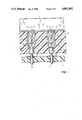
- FIG. 1 is a side sectional view of a device according to the invention
- FIG. 2 is a perspective view of crossing spring elements usable with the invention
- FIG. 3 shows another embodiment of the crossing spring elements.
- FIG. 1 shows an electronic component 1 with pins 2. For better illustration only two pins are shown. Actually the electronic component has a multiplicity of pins.
- the electronic component 1 for example, can be an integrated circuit.
- the electrical contact of the pins 2 of the integrated circuit shown in FIG. 1 can be made by a board 3.
- the board 3 is, for example, a printed wiring board (PW board).
- the PW board 3 has a thickness of approximately 3 to 4 mm.
- the PW board 3 has openings 4 which will receive and hold the pins 2 and connect to the pins 2.
- a plurality of spring elements (5', 5") are responsible for maintaining contact with the pins 2. Two of these elements (5', 5") are situated in the opening (4) and are shown in FIG. 1. More than two of the spring elements (5', 5") can be used in this configuration.
- the spring elements (5', 5") could be constructed from metal strips 2 to 3 mm wide and 0.5 to 1 mm thick. Copper alloy could be just one of the many types of material used.
- the spring elements are "S" shaped.
- the spring elements (5', 5") extend axially and are bowed radially outwardly in a center portion (6). Because of the elasticity of the material, the spring elements (5', 5") are kept in position by being forced inwardly by the pin 2 against the inside wall of the opening 4.
- the spring elements (5', 5") are directed toward each other but in the area of the top of the opening 4, the spring elements (5', 5") are directed away from each other to accommodate pin entry.
- the spring elements (5', 5") are separated by the inserted pin 2.
- the inserted pin 2 may be inserted into the opening 4 down to the area 8 where the two spring elements (5', 5") are located at the same level.
- a converging of the two spring elements (5', 5") is possible only if one (5') of the two spring elements (5', 5") has a slot for entry of a tapered end of the other element (5") (FIG. 2), or as shown in FIG. 3, where both spring elements (5', 5" have a tapered cross section which will allow convergence thereof.
- the two spring elements 5' and 5" shown in FIG. 1 are configured in the opening (4) so that the inserted pin 2 is pressing against the crossover location 8 of the spring elements (5', 5").
- the pressure generated by inserting the pin in the crossover area 8 of the two spring elements (5', 5") is transferred to the upper ends 7 of the spring elements (5', 5") and will generate pressure against the pin 2.
- the pressure generated by the spring elements (5', 5") will keep the pin 2 at a fixed location in the opening.
- An inner wall 9 bounding the opening 4 consists of a layer of metal.
- metal pins (10) are present which will conduct electrical current via the inner wall 9 composed of a metal shell or layer and the spring elements (5', 5") from the pin 2.
- the pins (10) can be inserted according to FIG. 1 in to the holes of a printed circuit board (11).
- the openings (4) in the region below the spring elements (5', 5") are filled with a metal member (12).
- the length of the spring elements (5', 5") will be matched to the length of the inserted pins 2. In the instance where the spring elements (5', 5") are crossed, the crossing point will move downwards as the pin is inserted.
- the board 3 can be produced in the following manner.
- the basic material of the board is an electrically isolating material.
- the body of the board 3 is provided with through holes. These holes are lined with metal casing to form the inner walls 9 which will conduct signals to or from the spring elements (5', 5").
- the isolating material also contains metal paths by which signals are conducted from one part of the board to another.
Abstract
Description
Claims (5)
Priority Applications (2)
| Application Number | Priority Date | Filing Date | Title |
|---|---|---|---|
| US07/207,879 US4892492A (en) | 1988-06-17 | 1988-06-17 | Device with openings for receiving pins of electrical components |
| EP19890110939 EP0346916A3 (en) | 1988-06-17 | 1989-06-16 | Device with openings for receiving pins of electrical components |
Applications Claiming Priority (1)
| Application Number | Priority Date | Filing Date | Title |
|---|---|---|---|
| US07/207,879 US4892492A (en) | 1988-06-17 | 1988-06-17 | Device with openings for receiving pins of electrical components |
Publications (1)
| Publication Number | Publication Date |
|---|---|
| US4892492A true US4892492A (en) | 1990-01-09 |
Family
ID=22772362
Family Applications (1)
| Application Number | Title | Priority Date | Filing Date |
|---|---|---|---|
| US07/207,879 Expired - Fee Related US4892492A (en) | 1988-06-17 | 1988-06-17 | Device with openings for receiving pins of electrical components |
Country Status (2)
| Country | Link |
|---|---|
| US (1) | US4892492A (en) |
| EP (1) | EP0346916A3 (en) |
Cited By (11)
| Publication number | Priority date | Publication date | Assignee | Title |
|---|---|---|---|---|
| US5038467A (en) * | 1989-11-09 | 1991-08-13 | Advanced Interconnections Corporation | Apparatus and method for installation of multi-pin components on circuit boards |
| US5059135A (en) * | 1990-06-06 | 1991-10-22 | Yamaichi Electric Mfg. Co., Ltd. | Contact in a socket for an electric part |
| US5597332A (en) * | 1993-08-06 | 1997-01-28 | Grote & Hartmann Gmbh & Co. Kg | Solder contact |
| US5645459A (en) * | 1994-03-16 | 1997-07-08 | Burndy Corporation | Electrical connector with female contact section having dual contact areas and stationary housing mounts |
| US5911606A (en) * | 1996-03-01 | 1999-06-15 | Advantest Corporation | Pin connector, pin connector holder and packaging board for mounting electronic component |
| US20120236523A1 (en) * | 2011-03-18 | 2012-09-20 | Fujitsu Limited | Board unit and method of fabricating the same |
| US20130143451A1 (en) * | 2011-05-20 | 2013-06-06 | Jianfeng Wu | Electrical Connector Terminal |
| US8998657B1 (en) * | 2011-01-14 | 2015-04-07 | Reliance Controls Corporation | High current female electrical contact assembly |
| US9054447B1 (en) | 2013-11-14 | 2015-06-09 | Reliance Controls Corporation | Electrical connector using air heated by an electrical arc during disengagement of contacts to extinguish the electrical arc |
| US20190199029A1 (en) * | 2017-12-21 | 2019-06-27 | Lotes Co., Ltd | Electrical connector |
| US10535946B2 (en) * | 2018-04-24 | 2020-01-14 | Lotes Co., Ltd | Electrical connector |
Families Citing this family (1)
| Publication number | Priority date | Publication date | Assignee | Title |
|---|---|---|---|---|
| FR2911222B1 (en) * | 2007-01-09 | 2013-04-26 | Legrand France | CONNECTION TERMINAL WITH DOUBLE SUPPORT. |
Citations (5)
| Publication number | Priority date | Publication date | Assignee | Title |
|---|---|---|---|---|
| US3407379A (en) * | 1966-05-11 | 1968-10-22 | Taiyo Yuden Kabushikikaisha | Multi-connector |
| US3980377A (en) * | 1975-08-25 | 1976-09-14 | Gte Laboratories Incorporated | Printed circuit connector |
| US4002400A (en) * | 1975-08-01 | 1977-01-11 | E. I. Du Pont De Nemours And Company | Electrical connector |
| EP0000163A1 (en) * | 1977-06-24 | 1979-01-10 | Grote & Hartmann GmbH & Co. KG | Cable lug with spring |
| US4647140A (en) * | 1984-04-04 | 1987-03-03 | Hewlett Packard Company | Electrical connectors |
Family Cites Families (3)
| Publication number | Priority date | Publication date | Assignee | Title |
|---|---|---|---|---|
| FR1456535A (en) * | 1965-06-23 | 1966-07-08 | Improvements in electrical contact sockets with inclined elastic wires, and in processes and machines for their manufacture | |
| US4505531A (en) * | 1983-08-29 | 1985-03-19 | Miller Edwin A | Socket terminal and connector |
| US4620757A (en) * | 1984-12-26 | 1986-11-04 | Brintec Systems Corporation | Connector socket |
-
1988
- 1988-06-17 US US07/207,879 patent/US4892492A/en not_active Expired - Fee Related
-
1989
- 1989-06-16 EP EP19890110939 patent/EP0346916A3/en not_active Withdrawn
Patent Citations (5)
| Publication number | Priority date | Publication date | Assignee | Title |
|---|---|---|---|---|
| US3407379A (en) * | 1966-05-11 | 1968-10-22 | Taiyo Yuden Kabushikikaisha | Multi-connector |
| US4002400A (en) * | 1975-08-01 | 1977-01-11 | E. I. Du Pont De Nemours And Company | Electrical connector |
| US3980377A (en) * | 1975-08-25 | 1976-09-14 | Gte Laboratories Incorporated | Printed circuit connector |
| EP0000163A1 (en) * | 1977-06-24 | 1979-01-10 | Grote & Hartmann GmbH & Co. KG | Cable lug with spring |
| US4647140A (en) * | 1984-04-04 | 1987-03-03 | Hewlett Packard Company | Electrical connectors |
Cited By (15)
| Publication number | Priority date | Publication date | Assignee | Title |
|---|---|---|---|---|
| US5038467A (en) * | 1989-11-09 | 1991-08-13 | Advanced Interconnections Corporation | Apparatus and method for installation of multi-pin components on circuit boards |
| US5059135A (en) * | 1990-06-06 | 1991-10-22 | Yamaichi Electric Mfg. Co., Ltd. | Contact in a socket for an electric part |
| US5597332A (en) * | 1993-08-06 | 1997-01-28 | Grote & Hartmann Gmbh & Co. Kg | Solder contact |
| US5645459A (en) * | 1994-03-16 | 1997-07-08 | Burndy Corporation | Electrical connector with female contact section having dual contact areas and stationary housing mounts |
| US5911606A (en) * | 1996-03-01 | 1999-06-15 | Advantest Corporation | Pin connector, pin connector holder and packaging board for mounting electronic component |
| USRE37961E1 (en) * | 1996-03-01 | 2003-01-07 | Advantest Corporation | Pin connector, pin connector holder and packaging board for mounting electronic component |
| US8998657B1 (en) * | 2011-01-14 | 2015-04-07 | Reliance Controls Corporation | High current female electrical contact assembly |
| US8901434B2 (en) * | 2011-03-18 | 2014-12-02 | Fujitsu Limited | Board unit and method of fabricating the same |
| US20120236523A1 (en) * | 2011-03-18 | 2012-09-20 | Fujitsu Limited | Board unit and method of fabricating the same |
| US20130143451A1 (en) * | 2011-05-20 | 2013-06-06 | Jianfeng Wu | Electrical Connector Terminal |
| US9735490B2 (en) * | 2011-05-20 | 2017-08-15 | Tyco Electronics (Shanghai) Co. Ltd. | Electrical connector terminal |
| US9054447B1 (en) | 2013-11-14 | 2015-06-09 | Reliance Controls Corporation | Electrical connector using air heated by an electrical arc during disengagement of contacts to extinguish the electrical arc |
| US20190199029A1 (en) * | 2017-12-21 | 2019-06-27 | Lotes Co., Ltd | Electrical connector |
| US10784613B2 (en) * | 2017-12-21 | 2020-09-22 | Lotes Co., Ltd | Electrical connector |
| US10535946B2 (en) * | 2018-04-24 | 2020-01-14 | Lotes Co., Ltd | Electrical connector |
Also Published As
| Publication number | Publication date |
|---|---|
| EP0346916A3 (en) | 1991-06-12 |
| EP0346916A2 (en) | 1989-12-20 |
Similar Documents
| Publication | Publication Date | Title |
|---|---|---|
| US6234827B1 (en) | Electrical connector shield with dual function of mechanical locking and electrical shielding continuety | |
| US4359258A (en) | Electrical connector | |
| US5425658A (en) | Card edge connector with reduced contact pitch | |
| US5613860A (en) | Universal grounding clip for card-receiving connector | |
| EP0228278A2 (en) | Electrical connector assembly | |
| US20070123109A1 (en) | High speed, card edge connector | |
| US4892492A (en) | Device with openings for receiving pins of electrical components | |
| EP1058352B1 (en) | Electrical connector | |
| US6475005B2 (en) | Electrical card connector | |
| US4538878A (en) | Solderless circuit board connector | |
| JPH0329282A (en) | Rib cage terminal | |
| US6749440B1 (en) | Electrical contact with dual electrical paths | |
| JPH02168581A (en) | Electric connector | |
| EP0673078A1 (en) | Insulation displacement contact terminal | |
| US5009606A (en) | Separable electrical connector | |
| US3871738A (en) | Fuse contacts | |
| US7182607B2 (en) | LGA socket connector having guiding means | |
| EP0047095A2 (en) | A connector for a leadless electronic package | |
| US6916186B2 (en) | Eletrical contact with dual electrical paths | |
| US6361365B1 (en) | Electrical connector having connected grounding plate and grounding pins | |
| US7063571B2 (en) | Smart card connector | |
| US4634200A (en) | Low profile stacking connector for printed circuit boards | |
| US4878849A (en) | Electrical connector having multi-position housing | |
| US7097517B2 (en) | Socket connector for integrated circuit | |
| US6210177B1 (en) | Electrical connector |
Legal Events
| Date | Code | Title | Description |
|---|---|---|---|
| AS | Assignment |
Owner name: MODULAR COMPUTER SYSTEMS, INC., 1650 WEST MCNAB RO Free format text: ASSIGNMENT OF ASSIGNORS INTEREST.;ASSIGNOR:MUELLER, HARRY B.;REEL/FRAME:004900/0998 Effective date: 19880614 Owner name: MODULAR COMPUTER SYSTEMS, INC., A FLORIDA CORP.,FL Free format text: ASSIGNMENT OF ASSIGNORS INTEREST;ASSIGNOR:MUELLER, HARRY B.;REEL/FRAME:004900/0998 Effective date: 19880614 |
|
| REMI | Maintenance fee reminder mailed | ||
| AS | Assignment |
Owner name: MODULAR COMPUTER SYSTEMS, INC. A FLORIDA CORPORA Free format text: ASSIGNMENT OF ASSIGNORS INTEREST;ASSIGNOR:MODULAR COMPUTER SYSTEMS II, INC. A FLORIDA CORPORATION;REEL/FRAME:006723/0992 Effective date: 19931007 |
|
| LAPS | Lapse for failure to pay maintenance fees | ||
| FP | Lapsed due to failure to pay maintenance fee |
Effective date: 19940109 |
|
| STCH | Information on status: patent discontinuation |
Free format text: PATENT EXPIRED DUE TO NONPAYMENT OF MAINTENANCE FEES UNDER 37 CFR 1.362 |