EP0346916A2 - Device with openings for receiving pins of electrical components - Google Patents
Device with openings for receiving pins of electrical components Download PDFInfo
- Publication number
- EP0346916A2 EP0346916A2 EP89110939A EP89110939A EP0346916A2 EP 0346916 A2 EP0346916 A2 EP 0346916A2 EP 89110939 A EP89110939 A EP 89110939A EP 89110939 A EP89110939 A EP 89110939A EP 0346916 A2 EP0346916 A2 EP 0346916A2
- Authority
- EP
- European Patent Office
- Prior art keywords
- spring
- opening
- spring elements
- sidewall
- pin
- Prior art date
- Legal status (The legal status is an assumption and is not a legal conclusion. Google has not performed a legal analysis and makes no representation as to the accuracy of the status listed.)
- Withdrawn
Links
Images

Classifications
-
- H—ELECTRICITY
- H01—ELECTRIC ELEMENTS
- H01R—ELECTRICALLY-CONDUCTIVE CONNECTIONS; STRUCTURAL ASSOCIATIONS OF A PLURALITY OF MUTUALLY-INSULATED ELECTRICAL CONNECTING ELEMENTS; COUPLING DEVICES; CURRENT COLLECTORS
- H01R12/00—Structural associations of a plurality of mutually-insulated electrical connecting elements, specially adapted for printed circuits, e.g. printed circuit boards [PCB], flat or ribbon cables, or like generally planar structures, e.g. terminal strips, terminal blocks; Coupling devices specially adapted for printed circuits, flat or ribbon cables, or like generally planar structures; Terminals specially adapted for contact with, or insertion into, printed circuits, flat or ribbon cables, or like generally planar structures
- H01R12/50—Fixed connections
- H01R12/51—Fixed connections for rigid printed circuits or like structures
- H01R12/55—Fixed connections for rigid printed circuits or like structures characterised by the terminals
- H01R12/58—Fixed connections for rigid printed circuits or like structures characterised by the terminals terminals for insertion into holes
-
- H—ELECTRICITY
- H01—ELECTRIC ELEMENTS
- H01R—ELECTRICALLY-CONDUCTIVE CONNECTIONS; STRUCTURAL ASSOCIATIONS OF A PLURALITY OF MUTUALLY-INSULATED ELECTRICAL CONNECTING ELEMENTS; COUPLING DEVICES; CURRENT COLLECTORS
- H01R4/00—Electrically-conductive connections between two or more conductive members in direct contact, i.e. touching one another; Means for effecting or maintaining such contact; Electrically-conductive connections having two or more spaced connecting locations for conductors and using contact members penetrating insulation
- H01R4/28—Clamped connections, spring connections
- H01R4/48—Clamped connections, spring connections utilising a spring, clip, or other resilient member
- H01R4/4809—Clamped connections, spring connections utilising a spring, clip, or other resilient member using a leaf spring to bias the conductor toward the busbar
- H01R4/48185—Clamped connections, spring connections utilising a spring, clip, or other resilient member using a leaf spring to bias the conductor toward the busbar adapted for axial insertion of a wire end
- H01R4/4819—Clamped connections, spring connections utilising a spring, clip, or other resilient member using a leaf spring to bias the conductor toward the busbar adapted for axial insertion of a wire end the spring shape allowing insertion of the conductor end when the spring is unbiased
- H01R4/4823—Multiblade spring
Definitions
- a device with openings for receiving pins of electrical components wherein in the openings spring elements are provided which are bowed in toward the center of the opening, then bowed out in the middle of the opening and drawn back towards the center of the opening at the top to form a funnel for receiving the pin.
- Figure 1 shows on the top an electronic component 1 with pins 2. For better illustration only two pins are shown. Actually the electronic component has a multi plicity of pins.
- the electronic component 1, for example, can be an integrated circuit.
- the electrical contact of the pin of the integrated circuit shown in figure 1 can be made by a board 3.
- the board 3 is, for example, a printed wiring board (PW board).
- the PW board 3 has a thickness of approximately 3 to 4 mm.
- the PW board 3 has openings 4 which will receive and hold the pins 2 and connect to the pins.
- the spring elements (5′, 5 ⁇ ) are responsible for maintaining contact with the pins 2. Two of these elements (5′, 5 ⁇ ) each situated in the opening (4) are shown in figure 1. More than two of the spring elements (5′, 5 ⁇ ) can be used in this configuration.
- the spring elements (5′, 5 ⁇ ) could be constructed from metal strips 2 to 3 mm wide and 0.5 to 1 mm thick. Copper alloy could be just one of the many types of material used.
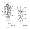
- the spring elements are "S" shaped. According to Figure 1, the spring elements (5′, 5 ⁇ ) are bowed outward in the center portion (6). Because of the elasticity of the material, the spring elements (5 5 ⁇ ) are kept in position by being forced inward against the inside wall of the opening. At the upper end (7) of the opening 4, the spring elements are directed toward each other but in the area of the top of the opening, the spring elements (5′, 5 ⁇ ) are directed away from each other to accommodate pin entry.
- the spring elements (5′, 5 ⁇ ) are separated by the inserted pin 2.
- the inserted pin 2 may be inserted into the opening down to the area 8 where the two spring elements (5′, 5 ⁇ ) are located at the same level.
- a converging of the two spring elements (5′, 5 ⁇ ) is possible only if one (5′) of the two elements (5′, 5 ⁇ ) has a slot for entry of a tapered end of the other element (5 ⁇ ) ( Figure 2), or as shown in Figure 3, both spring elements (5′ 5 ⁇ ) have a tapered crossection which will allow convergence.
- the two spring elements 5′ and 5 ⁇ shown in Figure 1 are configured in the opening (4) so that the inserted pin 2 is pressing against the crossover spring elements (5′ 5 ⁇ ).
- the pressure generated by inserting the pin in the crossover area 8 of the two spring elements (5′, 5 ⁇ ) is transferred to the upper area of the spring elements (5′, 5 ⁇ ) and will generate pressure against the pin 2.
- the pressure generated by the spring elements (5′, 5 ⁇ ) will keep the pin at a fixed location in the opening.
- the inner wall of the opening 4 consists of a layer of metal 9.
- metal pins (10) are present which will conduct electrical current via the metal shell or layer (9) and the spring elements (5′, 5 ⁇ ) from the pin 2.
- the pins (10) can be inserted according to Figure 1 in to the holes of a printed circuit board (11).
- the openings (4) in the region below the spring elements (5′, 5 ⁇ ) are filled with metal (12).
- the length of the spring elements (5′, 5 ⁇ ) will be matched to the length of the inserted pins 2. In the instance where the spring elements (5′, 5 ⁇ ) are crossed, the crossing point will move downwards as the pin is inserted.
- the board 3 will be produced in the following manner.
- the basic material of the board will be isolating material.
- the body of the board is provided with through holes. These holes are lined with metal casings which will conduct signal to or from the spring elements (5′, 5 ⁇ ).
- the isolating material also contains metal paths by which signals are conducted from one part of the board to another.
Landscapes
- Coupling Device And Connection With Printed Circuit (AREA)
- Connection Or Junction Boxes (AREA)
- Connecting Device With Holders (AREA)
- Portable Nailing Machines And Staplers (AREA)
Abstract
Description
- Electronic Components used in Computer Technology usually have multiple contacts (pins) for interconnection. To connect the contacts (pins) a certain connecting technology is necessary.
- It is the object of the invention to provide a device to connect and hold the pins of electronic components as for instance integrated circuits in a simple and reliable manner. According to the invention there is provided a device with openings for receiving pins of electrical components, wherein in the openings spring elements are provided which are bowed in toward the center of the opening, then bowed out in the middle of the opening and drawn back towards the center of the opening at the top to form a funnel for receiving the pin.
-
- Figure 1 shows a device according to the invention;
- Figure 2 shows the crossing spring elements;
- Figure 3 shows the crossing spring elements in another version.
- Figure 1 shows on the top an
electronic component 1 withpins 2. For better illustration only two pins are shown. Actually the electronic component has a multi plicity of pins. Theelectronic component 1, for example, can be an integrated circuit. The electrical contact of the pin of the integrated circuit shown in figure 1 can be made by a board 3. The board 3 is, for example, a printed wiring board (PW board). The PW board 3 has a thickness of approximately 3 to 4 mm. In accordance to figure 1 the PW board 3 hasopenings 4 which will receive and hold thepins 2 and connect to the pins. - The spring elements (5′, 5˝) are responsible for maintaining contact with the
pins 2. Two of these elements (5′, 5˝) each situated in the opening (4) are shown in figure 1. More than two of the spring elements (5′, 5˝) can be used in this configuration. The spring elements (5′, 5˝) could be constructed frommetal strips 2 to 3 mm wide and 0.5 to 1 mm thick. Copper alloy could be just one of the many types of material used. - As shown in Figure 1, the spring elements are "S" shaped. According to Figure 1, the spring elements (5′, 5˝) are bowed outward in the center portion (6). Because of the elasticity of the material, the spring elements (5 5˝) are kept in position by being forced inward against the inside wall of the opening. At the upper end (7) of the
opening 4, the spring elements are directed toward each other but in the area of the top of the opening, the spring elements (5′, 5˝) are directed away from each other to accommodate pin entry. - When the
pins 2 are inserted in the funnel shaped opening, the spring elements (5′, 5˝) are separated by the insertedpin 2. The insertedpin 2 may be inserted into the opening down to thearea 8 where the two spring elements (5′, 5˝) are located at the same level. A converging of the two spring elements (5′, 5˝) is possible only if one (5′) of the two elements (5′, 5˝) has a slot for entry of a tapered end of the other element (5˝) (Figure 2), or as shown in Figure 3, both spring elements (5′ 5˝) have a tapered crossection which will allow convergence. - The two
spring elements 5′ and 5˝ shown in Figure 1 are configured in the opening (4) so that the insertedpin 2 is pressing against the crossover spring elements (5′ 5˝). The pressure generated by inserting the pin in thecrossover area 8 of the two spring elements (5′, 5˝) is transferred to the upper area of the spring elements (5′, 5˝) and will generate pressure against thepin 2. The pressure generated by the spring elements (5′, 5˝), will keep the pin at a fixed location in the opening. - The inner wall of the
opening 4 consists of a layer ofmetal 9. At the lower end of theopening 4, metal pins (10) are present which will conduce electrical current via the metal shell or layer (9) and the spring elements (5′, 5˝) from thepin 2. The pins (10) can be inserted according to Figure 1 in to the holes of a printed circuit board (11). In order to further electrical contact between the printed circuit board and the component the openings (4) in the region below the spring elements (5′, 5˝) are filled with metal (12). - The length of the spring elements (5′, 5˝) will be matched to the length of the inserted
pins 2. In the instance where the spring elements (5′, 5˝) are crossed, the crossing point will move downwards as the pin is inserted. - The board 3 will be produced in the following manner. The basic material of the board will be isolating material. The body of the board is provided with through holes. These holes are lined with metal casings which will conduct signal to or from the spring elements (5′, 5˝). In addition, the isolating material also contains metal paths by which signals are conducted from one part of the board to another.
Claims (5)
a substrate having an opening therein which extends axially into said substrate and which is bounded by an electrically conductive sidewall, said opening having a mouth, a central axis, an upper portion and a lower portion; said sidewall having a lower concave portion and a lip projecting generally radially inwardly adjacent said mouth of said opening;
a pair of spring elements disposed within said opening which are in facing relationship to each other, each of said spring elements having an upper end portion, a center portion, and a terminal portion;
said terminal portion of each said spring being disposed in said lower portion of said opening in engagement with said concave portion of said sidewall so as to retain said terminal portion of said spring in a fixed axial position, each said spring extending generally axially from a first side of said opening across said central axis to the opposite side of said opening, both of said spring elements crossing said central axis at substantially common location; and
each said spring having a substantially sheet-like body, said terminal portion of each said contacting said sidewall in the vicinity of said lower portion of said opening, said upper end portion of each said spring engaging said lip of said sidewall in the vincinity of said upper portion of said opening so as to retain said spring within said opening, and said center portion of each said spring having a first portion which extends generally radially toward said central axis and a second portion which extends generally radially from said first portion toward said sidewall.
wherein said spring elements are fixed and held within said opening due to spring force which is generated by deformation of said spring elements within said opening due to insertion of a pin generally axially into said opening, wherein said spring elements are resiliently deformed from an initial position to a final position wherein said second portion of each said spring is in contacting spring-biased engagement with said sidewall and wherein said first portion of each said spring is in contacting spring-biased engangement with the pin.
wherein said upper end portions of each of said spring elements in said initial position cooperate to form a gap for receiving the pin such that the pin is in contact with both of said spring elements at said middle portion, and the spring pressure generated in at said terminal portions is transferred to said middle portion of said springs to exert increased pressure on the pin.
wherein one of said spring elements has a slot in its said terminal portion and said terminal portion of the other of said spring elements has a relatively reduced width and is disposed in said slot.
wherein said terminal portion of both said spring elements have a relatively reduced width.
Applications Claiming Priority (2)
| Application Number | Priority Date | Filing Date | Title |
|---|---|---|---|
| US207879 | 1980-11-18 | ||
| US07/207,879 US4892492A (en) | 1988-06-17 | 1988-06-17 | Device with openings for receiving pins of electrical components |
Publications (2)
| Publication Number | Publication Date |
|---|---|
| EP0346916A2 true EP0346916A2 (en) | 1989-12-20 |
| EP0346916A3 EP0346916A3 (en) | 1991-06-12 |
Family
ID=22772362
Family Applications (1)
| Application Number | Title | Priority Date | Filing Date |
|---|---|---|---|
| EP19890110939 Withdrawn EP0346916A3 (en) | 1988-06-17 | 1989-06-16 | Device with openings for receiving pins of electrical components |
Country Status (2)
| Country | Link |
|---|---|
| US (1) | US4892492A (en) |
| EP (1) | EP0346916A3 (en) |
Cited By (1)
| Publication number | Priority date | Publication date | Assignee | Title |
|---|---|---|---|---|
| FR2911222A1 (en) * | 2007-01-09 | 2008-07-11 | Legrand France | Double electrical connection terminal for electrical apparatus, has spring with support and butting strands which are arranged, such that tip is placed along direction introducing conductor in body, between input line and each butting stop |
Families Citing this family (11)
| Publication number | Priority date | Publication date | Assignee | Title |
|---|---|---|---|---|
| US5038467A (en) * | 1989-11-09 | 1991-08-13 | Advanced Interconnections Corporation | Apparatus and method for installation of multi-pin components on circuit boards |
| US5059135A (en) * | 1990-06-06 | 1991-10-22 | Yamaichi Electric Mfg. Co., Ltd. | Contact in a socket for an electric part |
| DE4326456A1 (en) * | 1993-08-06 | 1995-02-09 | Grote & Hartmann | Solder contact |
| US5645459A (en) * | 1994-03-16 | 1997-07-08 | Burndy Corporation | Electrical connector with female contact section having dual contact areas and stationary housing mounts |
| JP3735404B2 (en) * | 1996-03-01 | 2006-01-18 | 株式会社アドバンテスト | Semiconductor device measurement substrate |
| US8998657B1 (en) * | 2011-01-14 | 2015-04-07 | Reliance Controls Corporation | High current female electrical contact assembly |
| JP5686009B2 (en) * | 2011-03-18 | 2015-03-18 | 富士通株式会社 | Substrate unit and method for manufacturing substrate unit |
| CN102790308B (en) * | 2011-05-20 | 2015-08-12 | 泰科电子(上海)有限公司 | Electric connector terminal |
| US9054447B1 (en) | 2013-11-14 | 2015-06-09 | Reliance Controls Corporation | Electrical connector using air heated by an electrical arc during disengagement of contacts to extinguish the electrical arc |
| CN111048924A (en) * | 2017-12-21 | 2020-04-21 | 番禺得意精密电子工业有限公司 | Electrical connector |
| CN108767520B (en) * | 2018-04-24 | 2019-10-01 | 番禺得意精密电子工业有限公司 | Electric connector |
Family Cites Families (8)
| Publication number | Priority date | Publication date | Assignee | Title |
|---|---|---|---|---|
| FR1456535A (en) * | 1965-06-23 | 1966-07-08 | Improvements in electrical contact sockets with inclined elastic wires, and in processes and machines for their manufacture | |
| US3407379A (en) * | 1966-05-11 | 1968-10-22 | Taiyo Yuden Kabushikikaisha | Multi-connector |
| US4002400A (en) * | 1975-08-01 | 1977-01-11 | E. I. Du Pont De Nemours And Company | Electrical connector |
| US3980377A (en) * | 1975-08-25 | 1976-09-14 | Gte Laboratories Incorporated | Printed circuit connector |
| DE2728423A1 (en) * | 1977-06-24 | 1979-01-04 | Grote & Hartmann | SPRING LUG |
| US4505531A (en) * | 1983-08-29 | 1985-03-19 | Miller Edwin A | Socket terminal and connector |
| GB8408614D0 (en) * | 1984-04-04 | 1984-05-16 | Hewlett Packard Ltd | Electrical connectors |
| US4620757A (en) * | 1984-12-26 | 1986-11-04 | Brintec Systems Corporation | Connector socket |
-
1988
- 1988-06-17 US US07/207,879 patent/US4892492A/en not_active Expired - Fee Related
-
1989
- 1989-06-16 EP EP19890110939 patent/EP0346916A3/en not_active Withdrawn
Cited By (2)
| Publication number | Priority date | Publication date | Assignee | Title |
|---|---|---|---|---|
| FR2911222A1 (en) * | 2007-01-09 | 2008-07-11 | Legrand France | Double electrical connection terminal for electrical apparatus, has spring with support and butting strands which are arranged, such that tip is placed along direction introducing conductor in body, between input line and each butting stop |
| EP1944833A3 (en) * | 2007-01-09 | 2009-08-19 | Legrand France | Connection terminal with double support |
Also Published As
| Publication number | Publication date |
|---|---|
| US4892492A (en) | 1990-01-09 |
| EP0346916A3 (en) | 1991-06-12 |
Similar Documents
| Publication | Publication Date | Title |
|---|---|---|
| US6607400B1 (en) | Low profile RF connector assembly | |
| US6126464A (en) | Card connector having switching means | |
| US6168448B1 (en) | Audio jack connector | |
| US4808113A (en) | Connector for flexible flat cable | |
| US6729890B2 (en) | Reduced-size board-to-board connector | |
| US5613860A (en) | Universal grounding clip for card-receiving connector | |
| US6431893B1 (en) | Switch for an electrical card connector | |
| EP0228278A2 (en) | Electrical connector assembly | |
| US6322397B1 (en) | Miniaturized power jack with high normal force | |
| US6368156B1 (en) | Audio jack conveniently and reliably mounted on a circuit board | |
| EP0346916A2 (en) | Device with openings for receiving pins of electrical components | |
| US6475005B2 (en) | Electrical card connector | |
| KR20050040810A (en) | Connector for card | |
| US4538878A (en) | Solderless circuit board connector | |
| WO1991001051A1 (en) | Electrical connectors | |
| US20050037642A1 (en) | Electrical connector | |
| US6749440B1 (en) | Electrical contact with dual electrical paths | |
| US6478586B1 (en) | Electrical connector having conductive terminals that are provided with a dielectric coating | |
| US5973924A (en) | Symmetric multi-processor-package design | |
| US6067710A (en) | Method for manufacturing a memory card electrical connector with contacts having a ground terminal | |
| US6354876B1 (en) | Electronic card connector having improved grounding plate | |
| US6511349B2 (en) | Connection-retaining unit | |
| US20030232517A1 (en) | Electrical connector assembly | |
| US7063571B2 (en) | Smart card connector | |
| WO2002054540A1 (en) | Reduced-size board-to-board connector |
Legal Events
| Date | Code | Title | Description |
|---|---|---|---|
| PUAI | Public reference made under article 153(3) epc to a published international application that has entered the european phase |
Free format text: ORIGINAL CODE: 0009012 |
|
| AK | Designated contracting states |
Kind code of ref document: A2 Designated state(s): AT BE CH DE ES FR GB GR IT LI LU NL SE |
|
| RBV | Designated contracting states (corrected) |
Designated state(s): DE FR GB |
|
| PUAL | Search report despatched |
Free format text: ORIGINAL CODE: 0009013 |
|
| AK | Designated contracting states |
Kind code of ref document: A3 Designated state(s): AT BE CH DE ES FR GB GR IT LI LU NL SE |
|
| 17P | Request for examination filed |
Effective date: 19910606 |
|
| 17Q | First examination report despatched |
Effective date: 19920610 |
|
| STAA | Information on the status of an ep patent application or granted ep patent |
Free format text: STATUS: THE APPLICATION IS DEEMED TO BE WITHDRAWN |
|
| 18D | Application deemed to be withdrawn |
Effective date: 19921021 |