US5535153A - Semiconductor device - Google Patents
Semiconductor device Download PDFInfo
- Publication number
- US5535153A US5535153A US08/322,347 US32234794A US5535153A US 5535153 A US5535153 A US 5535153A US 32234794 A US32234794 A US 32234794A US 5535153 A US5535153 A US 5535153A
- Authority
- US
- United States
- Prior art keywords
- layer
- interconnections
- semiconductor device
- cell arrays
- sense amplifiers
- Prior art date
- Legal status (The legal status is an assumption and is not a legal conclusion. Google has not performed a legal analysis and makes no representation as to the accuracy of the status listed.)
- Expired - Lifetime
Links
Images


Classifications
-
- G—PHYSICS
- G11—INFORMATION STORAGE
- G11C—STATIC STORES
- G11C5/00—Details of stores covered by group G11C11/00
- G11C5/06—Arrangements for interconnecting storage elements electrically, e.g. by wiring
-
- G—PHYSICS
- G11—INFORMATION STORAGE
- G11C—STATIC STORES
- G11C11/00—Digital stores characterised by the use of particular electric or magnetic storage elements; Storage elements therefor
- G11C11/21—Digital stores characterised by the use of particular electric or magnetic storage elements; Storage elements therefor using electric elements
- G11C11/34—Digital stores characterised by the use of particular electric or magnetic storage elements; Storage elements therefor using electric elements using semiconductor devices
- G11C11/40—Digital stores characterised by the use of particular electric or magnetic storage elements; Storage elements therefor using electric elements using semiconductor devices using transistors
- G11C11/401—Digital stores characterised by the use of particular electric or magnetic storage elements; Storage elements therefor using electric elements using semiconductor devices using transistors forming cells needing refreshing or charge regeneration, i.e. dynamic cells
- G11C11/4063—Auxiliary circuits, e.g. for addressing, decoding, driving, writing, sensing or timing
- G11C11/407—Auxiliary circuits, e.g. for addressing, decoding, driving, writing, sensing or timing for memory cells of the field-effect type
- G11C11/409—Read-write [R-W] circuits
Definitions
- the present invention relates to a semiconductor device, and more particularly to a dynamic memory semiconductor device including shared sense amplifiers.
- One known dynamic memory semiconductor device disclosed in Japanese patent application No. 55-41622 has a plurality of sense amplifiers sharing a column decoder circuit which produces a selective signal for controlling switches between the sense amplifiers and data output lines.
- the area of the dynamic memory semiconductor device is prevented from being increased when implemented in a large-scale configuration because the number of column decoders can be reduced.
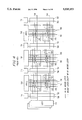
- FIGS. 1 through 5 of the accompanying drawings show the layouts of some conventional semiconductor devices with shared sense amplifiers.
- the conventional semiconductor devices are classified into several types according to the resistance of the material used of interconnections and the scale of the semiconductor device.
- FIG. 1 shows the layout of a first conventional semiconductor device.
- the conventional semiconductor device shown in FIG. 1 has interconnections made up of three layers, i.e., a polycrystalline silicon layer, a silicide layer, and a metallic layer. More specifically, word lines 401 are formed from the polycrystalline silicon layer and shared by the gate electrodes of MIS (Metal Insulator Semiconductor) transistors of memory cells 402. Bit lines 403 and interconnections (hereinafter referred to as "Y switches") 404 for transmitting selective signals from column decoders are formed from the silicide layer. One Y switch 404 is provided with respect to every four or eight bit lines 403.
- MIS Metal Insulator Semiconductor
- the metallic layer provides word-backing interconnections 406 disposed on cell arrays 405 for the purpose of virtually reducing the resistance of the word lines 401, array signal lines 408 disposed on sense amplifiers 407 parallel to the word lines 401 for transmitting sense amplifier drive signals or the like, and interconnections in row decoders 409, column decoders 410, array signal drive circuits 411, and peripheral circuits.
- FIG. 2 shows the layout of a second conventional semiconductor device.
- the conventional semiconductor device shown in FIG. 2 has interconnections made up of three layers, i.e., a polycrystalline silicon layer and two metallic layers. Stated otherwise, the semiconductor device shown in FIG. 2 is equivalent to the semiconductor device shown in FIG. 1 where the silicide layer is replaced with a metallic layer. The resistance of Y switches 504 is reduced because they are composed of the metallic layer. Since more sense amplifiers can be connected than in the first conventional semiconductor device, the semiconductor device shown in FIG. 2 is more suitable for large-scale integration.
- FIG. 3 shows the layout of a third conventional semiconductor device.
- the conventional semiconductor device shown in FIG. 3 has interconnections made up of three layers, i.e., a laminated layer of polycrystalline silicon and silicide (hereinafter referred to as a "polycide layer"), a silicide layer, and a metallic layer. More specifically, word lines 601 are formed from the polycide layer and shared by the gate electrodes of MIS transistors of memory cells 602. Y switches 604 are formed from the silicide layer. Bit lines 603, array signal lines 608 disposed on sense amplifiers 607, interconnections in row decoders 609, column decoders 610, array signal drive circuits 611, and peripheral circuits are formed from the metallic layer.
- bit lines and the Y switches are formed from different layers, unlike the first and second conventional semiconductor devices, if the bit lines are fabricated by the same process, they can be narrowed in the absence of any Y switches in their layer, resulting in a reduction in the size of the memory cell arrays. Furthermore, since the Y switches 604 are arranged at wide intervals, their width may be greater than in the first conventional semiconductor device, and their resistance may be reduced for a larger storage capacity.
- the third conventional semiconductor device is less suitable for a larger storage capacity than the second conventional semiconductor device because the Y switches 604 have a greater resistance than those of the metallic layer in the second conventional semiconductor device.
- the word lines are constructed from the polycide layer for reducing the resistance of the word lines. Consequently, the resistance of the word lines is not lowered as much as for the word lines combined with the word-backing interconnections, and hence the number of cells that can be connected to the word lines cannot be increased.
- FIG. 4 shows the layout of a fourth conventional semiconductor device.
- the conventional semiconductor device shown in FIG. 4 has interconnections made up of four layers, i.e., a polycrystalline silicon layer, a silicide layer, and two metallic layers.
- the polycrystalline silicon layer may be replaced with a polycide layer.
- Word lines 701 are formed from the polycrystalline silicon layer or the polycide layer and shared by gate electrodes of MIS transistors of memory cells 702.
- Bit lines 703 are formed from the silicide layer.
- One of the metallic layers provides word-backing interconnections 706 disposed on cell arrays 705 parallel to word lines 701, and some interconnections in row decoders 709, column decoders 710, array signal drive circuits 711, and peripheral circuits.
- the other metallic layer provides Y switches 704 disposed on cell arrays 705 and sense amplifiers 707 perpendicular to word lines 701, and some interconnections in row decoders 709, column decoders 710, array signal drive circuits 711, and peripheral circuits. Since Y switches 704 and word-backing interconnections 706 are made from different metallic layers, the interconnections parallel and perpendicular to word lines 701 have a smaller resistance than those of the first, second, and third conventional semiconductor devices, making the fourth conventional semiconductor device suitable for a large-storage-capacity configuration.
- FIG. 5 shows the layout of a fifth conventional semiconductor device.
- the conventional semiconductor device shown in FIG. 5 has interconnections made up of four layers, i.e., a polycide layer, a silicide layer, and two metallic layers.
- Word lines 801 are formed from the polycide layer and shared by the gate electrodes of MIS transistors of memory cells 802.
- Bit lines 803 are formed from the silicide layer.
- One of the metallic layers provides main word lines 806 disposed on cell arrays 805 parallel to word lines 801, array signal lines 808 disposed on sense amplifiers 807 parallel to word lines 801, and some interconnections in row decoders 809, column decoders 810, array signal drive circuits 811, divided decoders 812, divided decoder drive circuits 813, and peripheral circuits.
- the other metallic layer provides Y switches 804 disposed on cell arrays 805 and sense amplifiers 807 perpendicularly to word lines 801, divided decoder drive signal lines 814 disposed on divided decoders 812 perpendicular to word lines 801, and some interconnections in row decoders 809, column decoders 810, array signal drive circuits 811, divided decoders 812, divided decoder drive circuits 813, and the peripheral circuits.
- the word-backing interconnections in the fourth conventional semiconductor device are dispensed with, and some of the row decoders are scattered as divided decoders 812 between cell arrays 805, divided decoders 812 and row decoders 809 are interconnected by main word lines 806, and a signal required to select word lines 801 in divided decoders 812 is received by divided decoder drive circuits 813 and divided decoder drive signal lines 814.
- K. Noda T. Saeki, A. Tsujimoto, T. Murotani, and K.
- FIG. 6 of the accompanying drawings illustrates the circuit of a conventional sense amplifier region.
- bit lines 903 and Y switches 904 lie parallel to each other, and array signal lines 908 including write data lines 921, write drive signal lines 922, read data lines 923, read drive signal lines 924, an N-channel sense amplifier drive signal line 925, and a P-channel sense amplifier drive signal line 926 lie perpendicular to bit lines 903.
- N-channel sense amplifier drive signal line 925 and P-channel sense amplifier drive signal line 926 are required to be in the form of metallic interconnections because they should be of a low resistance for passing currents for charging and discharging bit lines 903.
- the number of column decoders used is lowered to reduce any increase in the area of the semiconductor device which is caused by a large-storage-capacity arrangement thereof.
- the storage capacity increases from 1 Mbit to 4 Mbits to 16 Mbits to 64 Mbits, the number of sense amplifiers connected to one column decoder is increased. Therefore, it is necessary to reduce the resistance of the Y switches, and a metallic layer used for only the Y switches is needed on the cell arrays as with the fourth and fifth conventional semiconductor devices described above.
- the array signal lines on the sense amplifiers must also be formed from a low-resistance metallic layer as they pass a large current therethrough.
- the fourth and fifth conventional large-storage-capacity semiconductor devices with shared sense amplifiers employ four-layer interconnections other than a conductive layer for forming a capacitor.
- the process of fabricating such a semiconductor device entails an increased number of steps, and the yield of such a semiconductor device is low.
- a semiconductor device comprising a plurality of cell arrays each comprising a plurality of memory cells each composed of a MIS transistor and a capacitor formed by a conductive layer; a plurality of word lines and bit lines which intersect each other at the memory cells; a plurality of sense amplifiers alternating with the cell arrays; a plurality of row decoders; a plurality of column decoders, each of the column decoders being connected to and shared by a plurality of the sense amplifiers; a plurality of interconnections for transmitting selective signals from the word lines, the bit lines and the column decoders; the interconnections for transmitting selective signals from the bit lines and the column decoder extending in the direction in which the cell arrays and the sense amplifiers are arrayed; the interconnections for transmitting selective signals from the word lines, the bit lines and the column decoder being formed from three different layers, other than the conductive layer for forming a capacitor, on the cell arrays; and the inter
- the interconnections for transmitting selective signals from the column decoder may be formed from the metallic layer on the cell arrays and from a conductive layer, which is the same layer as for the plate electrodes of the capacitors, on the sense amplifiers.
- the three different layers may include: a first layer, which layer provides gate electrodes of the MIS transistors, comprises a laminated layer of polycrystalline silicon and silicide, and has a portion providing the word lines; a second layer which comprises a silicide layer or a laminated layer of polycrystalline silicon and silicide and has a portion providing the bit lines; and a third layer which comprises a metallic layer and has a portion providing the interconnections on the cell arrays for transmitting selective signals from the column decoder.
- the semiconductor device may further comprise a plurality of power supply lines and a plurality of ground lines disposed on the cell arrays and the sense amplifiers between the interconnections for transmitting selective signals from the column decoder; a plurality of P-channel MOS transistors disposed in sense amplifier regions and having respective sources, drains and gates; a plurality of N-channel MOS transistors disposed in the sense amplifier regions and having respective sources, drains, and gates; the sense amplifiers comprising flip-flop sense amplifiers composed of P-channel transistors and having common sources and flip-flop sense amplifiers composed of N-channel transistors and having common sources; wherein the power supply lines are connected to the sources of the P-channel MOS transistors, the drains of the P-channel MOS transistors are connected to the common sources of the flip-flop sense amplifiers composed of P-channel transistors, and the gates of the P-channel MOS transistors are formed from the first layer of the three layers and serve as signal lines for activating the flip-flop sense amplifiers composed of P-channel transistors; and wherein
- the three different layers may include: a first layer which provides gate electrodes of the MIS transistors, comprises a laminated layer of polycrystalline silicon and silicide, and has a portion providing the word lines; a second layer which comprises a silicide layer or a laminated layer of polycrystalline silicon and silicide and has a portion providing the bit lines; and a third layer which comprises a metallic layer and has a portion providing the interconnections on the cell arrays and the sense amplifiers for transmitting selective signals from the column decoders.
- the three different layers may include: a first layer which provides gate electrodes of the MIS transistors, comprises a laminated layer of polycrystalline silicon and silicide, and has a portion providing the word lines; a second layer which comprises a metallic layer and has a portion providing the bit lines; and a third layer which comprises a metallic layer and has a portion providing the interconnections on the cell arrays and the sense amplifiers for transmitting selective signals from the column decoders.
- FIG. 1 is a block diagram showing the layout of a first conventional semiconductor device
- FIG. 2 is a block diagram showing the layout of a second conventional semiconductor device
- FIG. 3 is a block diagram showing the layout of a third conventional semiconductor device
- FIG. 4 is a block diagram showing the layout of a fourth conventional semiconductor device
- FIG. 5 is a block diagram showing the layout of a fifth conventional semiconductor device
- FIG. 6 is a circuit diagram of a conventional sense amplifier region
- FIG. 7 is a block diagram showing the layout of a semiconductor device according to a first embodiment of the present invention.
- FIG. 8(a) is a cross-sectional view of a pattern of Y switches in a sense amplifier region of the semiconductor device according to the first embodiment of the present invention
- FIG. 8(b) is a cross-sectional view of a memory cell of the semiconductor device according to the first embodiment of the present invention.
- FIG. 9 is a block diagram showing the layout of a semiconductor device according to a second embodiment of the present invention.
- FIG. 10 is a circuit diagram of a sense amplifier region of the semiconductor device according to the second embodiment of the present invention.
- FIG. 11 is a block diagram showing the layout of a semiconductor device according to a third embodiment of the present invention.
- a semiconductor device shown in FIGS. 7 and 8(a), 8(b) according to the first embodiment of the present invention has interconnections formed from three layers, i.e., a polycide layer, a silicide or polycide layer, and a metallic layer other than a conductive layer for forming a capacitor.
- the conductive layer for forming a capacitor comprises a polycrystalline silicon layer used as node electrodes 112 (see FIG. 8(b)) of the capacitors of memory cells 102 (see FIG. 7), and a polycide layer used as plate electrodes 113 (see FIGS. 8(a) and 8(b)) of the capacitors of memory cells 102.
- word lines 101 are formed from the polycide layer and shared by the gate electrodes of MIS transistors of memory cells 102.
- Bit lines 103 are formed from the silicide or polycide layer.
- Y switches 104 are formed from the metallic layer on cell arrays 105, and from the polycide layer on sense amplifiers 107 which is used as plate electrodes 113 of the capacitors of memory cells 102.
- the metallic layer provides array signal lines 108 disposed on the sense amplifiers 107 parallel to word lines 101, and interconnections in row decoders 109, a column decoder 110, array signal drive circuits 111, and peripheral circuits.
- the plate electrode 113 is positioned directly below the metallic layer. Therefore, in a sense amplifier region, the polycide layer, which is the same as the layer of plate electrode 113, is arranged as Y switch 104 in a pattern to avoid a connection hole through which the metallic layer of array signal line 108 is connected to a lower layer.
- FIGS. 9 and 10 A semiconductor device according to a second embodiment of the present invention will next be described with reference to FIGS. 9 and 10.
- the semiconductor device has interconnections formed from three layers, i.e., a polycide layer, a silicide or polycide layer, and a metallic layer other than a conductive layer for forming a capacitor.
- word lines 201 are formed from the polycide layer and are shared by the gate electrodes of MIS transistors of memory cells 202.
- Bit lines 203 are formed from the silicide or polycide layer.
- Y switches 204 are formed from the metallic layer on both cell arrays 205 and sense amplifiers 207.
- Array signal lines 208 disposed on sense amplifiers 207 are formed primarily from the polycide layer.
- the metallic layer provides interconnections in row decoders 209, a column decoder 210, array signal drive circuits 211 and peripheral circuits.
- Array signal lines 208 have a large resistance and cannot pass a sufficient current therethrough as they are formed primarily from the polycide layer.
- power supply lines (VCC) 231 and ground lines (GND) 232 are disposed on cell arrays 205 and sense amplifiers 207 between Y switches 204.
- power supply lines 231 are connected to the sources of P-channel MOS transistors in sense amplifier regions, the drains of the P-channel MOS transistors are connected to the common sources of flip-flop sense amplifiers composed of P-channel transistors, and the gates of P-channel MOS transistors are formed from the first polycide layer and serve as P-channel sense amplifier activating signal lines.
- Ground lines 232 are connected to the sources of N-channel MOS transistors in the sense amplifier regions, the drains of the N-channel MOS transistors are connected to the common sources of flip-flop sense amplifiers composed of N-channel transistors, and the gates of N-channel MOS transistors are formed from the first polycide layer and serve as N-channel sense amplifier activating signal lines.
- Power supply lines 231 and ground lines 232 must be formed from the low-resistance metallic layer in order to pass a large current therethrough, and extend parallel to Y switches 204. To prevent the interconnection pitch or spacing from being reduced by the positioning of power supply lines 231 and ground lines 232 between Y switches 204, the number of Y switches 204 is reduced to half, the number of sense amplifiers connected to each Y switch 204 is increased, and the number of write drive signal lines 222 and read data lines 223 are increased accordingly.
- a semiconductor device according to a third embodiment of the present invention will next be described with reference to FIG. 11.
- the semiconductor device has interconnections formed from three layers, i.e., a polycide layer, a first metallic layer, and a second metallic layer.
- word lines 301 are formed from the polycide layer and are shared by the gate electrodes of MIS transistors of memory cells 302.
- Bit lines 303 are formed from the first metallic layer on cell arrays 305 and primarily from the polycide layer on sense amplifiers 307.
- Y switches 304 are formed from the second metallic layer on both cell arrays 305 and sense amplifiers 307.
- the first and second metallic layers provide interconnections in row decoders 309, a column decoder 310, array signal drive circuits 311, and peripheral circuits.
- Array signal lines 308 are formed from the first metallic layer.
Landscapes
- Engineering & Computer Science (AREA)
- Microelectronics & Electronic Packaging (AREA)
- Computer Hardware Design (AREA)
- Semiconductor Memories (AREA)
- Dram (AREA)
- Static Random-Access Memory (AREA)
Abstract
Description
Claims (3)
Applications Claiming Priority (2)
| Application Number | Priority Date | Filing Date | Title |
|---|---|---|---|
| JP5-273682 | 1993-11-01 | ||
| JP5273682A JP2785655B2 (en) | 1993-11-01 | 1993-11-01 | Semiconductor device |
Publications (1)
| Publication Number | Publication Date |
|---|---|
| US5535153A true US5535153A (en) | 1996-07-09 |
Family
ID=17531085
Family Applications (1)
| Application Number | Title | Priority Date | Filing Date |
|---|---|---|---|
| US08/322,347 Expired - Lifetime US5535153A (en) | 1993-11-01 | 1994-10-13 | Semiconductor device |
Country Status (3)
| Country | Link |
|---|---|
| US (1) | US5535153A (en) |
| JP (1) | JP2785655B2 (en) |
| KR (1) | KR0142037B1 (en) |
Cited By (7)
| Publication number | Priority date | Publication date | Assignee | Title |
|---|---|---|---|---|
| US5640338A (en) * | 1995-12-07 | 1997-06-17 | Hyundai Electronics Industries Co. Ltd. | Semiconductor memory device |
| US5657265A (en) * | 1995-06-29 | 1997-08-12 | Samsung Electronics Co., Ltd. | Semiconductor memory device having circuit array structure for fast operation |
| US5793664A (en) * | 1996-01-25 | 1998-08-11 | Nec Corporation | Dynamic random access memory device |
| US6018172A (en) * | 1994-09-26 | 2000-01-25 | Mitsubishi Denki Kabushiki Kaisha | Semiconductor memory device including memory cell transistors formed on SOI substrate and having fixed body regions |
| US20080019172A1 (en) * | 2005-12-09 | 2008-01-24 | Macronix International Co., Ltd. | Gated Diode Nonvolatile Memory Cell Array |
| US20220077161A1 (en) * | 2020-09-04 | 2022-03-10 | Changxin Memory Technologies, Inc. | Semiconductor device |
| CN115132737A (en) * | 2022-07-28 | 2022-09-30 | 北京知存科技有限公司 | Semiconductor device array |
Families Citing this family (5)
| Publication number | Priority date | Publication date | Assignee | Title |
|---|---|---|---|---|
| JP3386924B2 (en) * | 1995-05-22 | 2003-03-17 | 株式会社日立製作所 | Semiconductor device |
| WO1998054727A2 (en) * | 1997-05-30 | 1998-12-03 | Micron Technology, Inc. | 256 Meg DYNAMIC RANDOM ACCESS MEMORY |
| DE19960558B4 (en) * | 1999-12-15 | 2008-07-24 | Qimonda Ag | Random Access Memory Type Random Access Memory (DRAM) |
| JP2001344966A (en) * | 2000-06-06 | 2001-12-14 | Toshiba Corp | Semiconductor storage device |
| JP5261003B2 (en) * | 2008-03-31 | 2013-08-14 | ローム株式会社 | Semiconductor memory device |
Citations (1)
| Publication number | Priority date | Publication date | Assignee | Title |
|---|---|---|---|---|
| US5361233A (en) * | 1990-05-25 | 1994-11-01 | Matsushita Electric Industrial Co., Ltd. | Semiconductor memory apparatus |
Family Cites Families (5)
| Publication number | Priority date | Publication date | Assignee | Title |
|---|---|---|---|---|
| JPS6054471A (en) * | 1983-09-05 | 1985-03-28 | Hitachi Ltd | semiconductor memory |
| JPS60246092A (en) * | 1984-05-21 | 1985-12-05 | Hitachi Ltd | semiconductor storage device |
| JPH02246090A (en) * | 1989-03-17 | 1990-10-01 | Fujitsu Ltd | Semiconductor storage device |
| JPH02236893A (en) * | 1990-02-23 | 1990-09-19 | Hitachi Ltd | semiconductor memory device |
| JPH0799620B2 (en) * | 1991-07-19 | 1995-10-25 | 株式会社日立製作所 | Semiconductor memory device |
-
1993
- 1993-11-01 JP JP5273682A patent/JP2785655B2/en not_active Expired - Fee Related
-
1994
- 1994-10-13 US US08/322,347 patent/US5535153A/en not_active Expired - Lifetime
- 1994-10-31 KR KR1019940028174A patent/KR0142037B1/en not_active Expired - Fee Related
Patent Citations (1)
| Publication number | Priority date | Publication date | Assignee | Title |
|---|---|---|---|---|
| US5361233A (en) * | 1990-05-25 | 1994-11-01 | Matsushita Electric Industrial Co., Ltd. | Semiconductor memory apparatus |
Non-Patent Citations (4)
| Title |
|---|
| K. Noda et al., "A Boosted Dual Word-line Decoding Scheme for 256Mb DRAMs," 1992 Symposium on VLSI Circuits Digest of Technical Papers, pp. 112-113. |
| K. Noda et al., A Boosted Dual Word line Decoding Scheme for 256Mb DRAMs, 1992 Symposium on VLSI Circuits Digest of Technical Papers, pp. 112 113. * |
| T. Sugibayashi et al., "WP 3.5: A 30ns 256Mb DRAM with Multi-Divided Array Structure," IEEE International Solid-State Circuits Conference, Feb. 24, 1993, pp. 50-51. |
| T. Sugibayashi et al., WP 3.5: A 30ns 256Mb DRAM with Multi Divided Array Structure, IEEE International Solid State Circuits Conference, Feb. 24, 1993, pp. 50 51. * |
Cited By (12)
| Publication number | Priority date | Publication date | Assignee | Title |
|---|---|---|---|---|
| US6018172A (en) * | 1994-09-26 | 2000-01-25 | Mitsubishi Denki Kabushiki Kaisha | Semiconductor memory device including memory cell transistors formed on SOI substrate and having fixed body regions |
| US6384445B1 (en) | 1994-09-26 | 2002-05-07 | Mitsubishi Denki Kabushiki Kaisha | Semiconductor memory device including memory cell transistors formed on SOI substrate and having fixed body regions |
| US5657265A (en) * | 1995-06-29 | 1997-08-12 | Samsung Electronics Co., Ltd. | Semiconductor memory device having circuit array structure for fast operation |
| US5640338A (en) * | 1995-12-07 | 1997-06-17 | Hyundai Electronics Industries Co. Ltd. | Semiconductor memory device |
| US5793664A (en) * | 1996-01-25 | 1998-08-11 | Nec Corporation | Dynamic random access memory device |
| US20080019172A1 (en) * | 2005-12-09 | 2008-01-24 | Macronix International Co., Ltd. | Gated Diode Nonvolatile Memory Cell Array |
| US7474558B2 (en) * | 2005-12-09 | 2009-01-06 | Macronix International Co., Ltd. | Gated diode nonvolatile memory cell array |
| US20090080254A1 (en) * | 2005-12-09 | 2009-03-26 | Macronix International Co., Ltd. | Gated Diode Nonvolatile Memory Cell Array |
| US7672157B2 (en) | 2005-12-09 | 2010-03-02 | Macronix International Co., Ltd. | Gated diode nonvolatile memory cell array |
| US20220077161A1 (en) * | 2020-09-04 | 2022-03-10 | Changxin Memory Technologies, Inc. | Semiconductor device |
| US12376291B2 (en) * | 2020-09-04 | 2025-07-29 | Changxin Memory Technologies, Inc. | Semiconductor device including shared sense amplification circuit group |
| CN115132737A (en) * | 2022-07-28 | 2022-09-30 | 北京知存科技有限公司 | Semiconductor device array |
Also Published As
| Publication number | Publication date |
|---|---|
| JP2785655B2 (en) | 1998-08-13 |
| KR0142037B1 (en) | 1998-07-15 |
| JPH07130164A (en) | 1995-05-19 |
| KR950015785A (en) | 1995-06-17 |
Similar Documents
| Publication | Publication Date | Title |
|---|---|---|
| US6288925B1 (en) | System with meshed power and signal buses on cell array | |
| US6600671B2 (en) | Reduced area sense amplifier isolation layout in a dynamic RAM architecture | |
| US4658377A (en) | Dynamic memory array with segmented bit lines | |
| US4709351A (en) | Semiconductor memory device having an improved wiring and decoder arrangement to decrease wiring delay | |
| EP0712132B1 (en) | Semiconductor memory | |
| US7323727B2 (en) | System with meshed power and signal buses on cell array | |
| US6392942B2 (en) | Semiconductor memory device having a multi-layer interconnection structure suitable for merging with logic | |
| US6191990B1 (en) | Semiconductor integrated circuit device having stabilizing capacitors connected between power lines of main amplifiers | |
| US6504770B2 (en) | Semiconductor memory | |
| US5535153A (en) | Semiconductor device | |
| US4554646A (en) | Semiconductor memory device | |
| KR100379289B1 (en) | Semiconductor Integrated Circuit Having Logic Circuit Comprising Transistor with Lower Threshold Voltage Values and Improved Pattern Layout | |
| US4701885A (en) | Dynamic memory array with quasi-folded bit lines | |
| US5182727A (en) | Array layout structure for implementing large high-density address decoders for gate array memories | |
| US6222784B1 (en) | Semiconductor memory | |
| US5598363A (en) | Semiconductor device having an improved reliability | |
| US6355982B2 (en) | Semiconductor memory device having pairs of bit lines arranged on both sides of memory cells | |
| US4908797A (en) | Dynamic memory array with quasi-folded bit lines | |
| US5877994A (en) | Space-efficient MDQ switch placement | |
| JPH0542077B2 (en) | ||
| US6512257B2 (en) | System with meshed power and signal buses on cell array | |
| KR20040041097A (en) | Sense amplifier and architecture for open digit arrays | |
| KR0163549B1 (en) | Memory device of sub-word line structure | |
| JPH11328951A (en) | Semiconductor storage device |
Legal Events
| Date | Code | Title | Description |
|---|---|---|---|
| AS | Assignment |
Owner name: NEC CORPORATION, JAPAN Free format text: ASSIGNMENT OF ASSIGNORS INTEREST;ASSIGNOR:SAEKI, TAKANORI;REEL/FRAME:007187/0531 Effective date: 19941004 |
|
| STCF | Information on status: patent grant |
Free format text: PATENTED CASE |
|
| FEPP | Fee payment procedure |
Free format text: PAYOR NUMBER ASSIGNED (ORIGINAL EVENT CODE: ASPN); ENTITY STATUS OF PATENT OWNER: LARGE ENTITY |
|
| FPAY | Fee payment |
Year of fee payment: 4 |
|
| AS | Assignment |
Owner name: NEC ELECTRONICS CORPORATION, JAPAN Free format text: ASSIGNMENT OF ASSIGNORS INTEREST;ASSIGNOR:NEC CORPORATION;REEL/FRAME:013798/0626 Effective date: 20021101 |
|
| FPAY | Fee payment |
Year of fee payment: 8 |
|
| FPAY | Fee payment |
Year of fee payment: 12 |
|
| AS | Assignment |
Owner name: RENESAS ELECTRONICS CORPORATION, JAPAN Free format text: CHANGE OF NAME;ASSIGNOR:NEC ELECTRONICS CORPORATION;REEL/FRAME:025149/0840 Effective date: 20100401 |