BACKGROUND OF THE INVENTION
1. Field of the Invention
The present invention relates to an analog/digital converter circuit (hereinafter abbreviated as an A/D converter circuit) for converting an analog signal to a digital signal, and more particularly the present invention relates to a serial/parallel type A/D converter circuit for converting an analog signal to a digital signal with two stages that form an upper data part and a lower data part.
2. Description of the Related Art
Various types of analog-to-digital conversion systems have been proposed, in one such system known as a parallel-type (flash-type) A/D converter the circuit quantizes the amplitude of the analog signal and converts the quantized signal to a digital code.
In such a parallel-type A/D converter circuit, high speed operation is possible, however when the number of the conversion bits is n, at least (2n -1) comparators are necessary for implementation of the circuit. A total of 255 comparators are necessary to obtain an 8-bit conversion code, and it is necessary to form several tens of thousands active elements by integration into a circuit in order to obtain a digital code having higher resolution.
For this reason, a parallel-type A/D converter circuit has the advantage that high speed processing is possible, but it is undesirable due to increases in which is required power consumption and the large surface area for the chip.
Therefore, a so-called serial/parallel type A/D converter circuit has been proposed in which, for conversion of the analog signal to n bits of resolution. In this circuit first the analog signal is digitized by rough quantization, so that an "a" bit conversion code including the most significant bit (MSB) is obtained, and in order to reduce the error of this upper data conversion code, that is, the quantization noise, the upper data quantization range is finely divided and digitized, so that the lower data [b (n-a)] bit conversion code including the lower significant bit (LSB) is obtained.
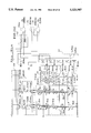
FIG. 1 is a structural view showing an outline of one such serial/parallel type A/D converter circuit which illustrates the circuit configuration for converting an analog signal to a 4-bit digital code.
In FIG. 1, R1 to R16 denote reference resistance elements serially connected between terminals of reference voltages VRT to VRB (0 to -2 V); Cu1 to Cu3 denote upper data comparators which have one input terminal connected to an input line of an input analog signal VIN to be converted and the other input terminal connected to the input line of the reference voltages (V4, V8, V12) of the rough quantization level divided by reference resistance elements R1 to R16 ; Bu1 to Bu3 denote buffers for obtaining the complementary outputs of the outputs of upper data comparators Cu1 to Cu3 ; Au1 to Au4 denote AND gates; Sa1 to Sa12 denote switching blocks arranged in the form of a matrix comprising four rows and three columns; Cd1 to Cd3 denote lower data comparators with one input terminal connected to the input line of the analog signal VIN and the other side input terminal connected to the output terminals of the switching blocks Sa1 to Sa12 ; Eu1 denotes an upper data encoder which encodes the result of differentiation of binary signals output from the upper data comparators Cu1 to Cu3 and converts the same to for example a 2-bit binary code (or complementary code of 2); and Ed1 denotes a lower data encoder which converts the result of differentiation of the binary signals output from the lower data comparators Cd1 to Cd3 to a 2-bit binary code; respectively.
The switching blocks Sa1 to Sa12 are controlled to turn on or off in accordance with the data "1" and "0" of the output level of the AND gates Au1 to Au4.
For example, when a signal of the "1" level is output from the AND gate Au1, control is performed so that the switching blocks Sa1 to Sa3 become an ON state; when the signal of the "1" level is output from the AND gate Au2, control is performed so that the switching blocks Sa4 to Sa6 become an ON state; when the signal of the "1" level is output from the AND gate Au3, control is performed so that the switching blocks Sa7 to Sa9 become an ON state; and when the signal of the "1" level is output from the AND gate Au4, control is performed so that the switching blocks Sa10 to Sa12 become an ON state;
In the serial/parallel type A/D converter circuit having such a structure, as shown in for example FIG. 2, the input analog signal VIN is sampled at the using point of the sampling pulse PS, and the sampling voltage VS thereof is supplied to the upper data encoder Eu1 and the lower data encoder Ed1.
At the upper data encoder Eu1, when the sampling voltage VS is supplied, the binary signal outputs of the upper data comparators Cu1 to Cu3 are converted to the code signals D0 and D1 of the upper significant 2 bits at the point of time TH of trailing edge (point of time lagged by τA) of the clock signal CLK and output.
At the lower data encoder Ed1, when the sampling voltage VS is supplied, the binary signal outputs of the lower data comparators Cd1 to Cd3 are converted to the code signals D2 and D3 of the lower significant 2 bits at the point of time TL of trailing (point of time lagged by τB) of the clock signal CLK,
Explaining this more concretely, reference voltages V4, V8, and V12 of the rough quantization level, divided by the reference resistance elements R1 to R16 and the input analog signal VIN are compared by the upper data comparators Cu1 to Cu3.
As a result of this comparison, for example, when V4 <VIN <V8, the output of the upper data comparator Cu3 becomes the high level at a high potential ("1"), and the outputs of the upper data comparators Cu2 and Cu3 become the low level at a low potential ("0").
Thus, at the output of the AND gates Au1 to Au4, only the output of the AND gate Au2 becomes "1", and the outputs of the other AND gates Au1, Au3, and Au4 become "0".
As a result, the code [01] is output as the upper significant 2 bits of the conversion code from the upper data encoder Eu1.
Next, in a state where the upper significant 2 bits of the conversion code are latched, the signal of the "1" level output from the AND gate Au2 is input to the switching blocks Sa4 to Sa6. By this, the switching blocks Sa4 to Sa6 become an ON state.
Along with the switching blocks Sa4 to Sa6 becoming the ON state, the sampled analog signal VIN existing at the level represented as V4 <VIN <V8 is further divided by the resistance elements R4 to R6, and regulated reference voltages V5, V6, and V7 are input via the switching blocks Sa4, Sa5, and Sa6 to the other input terminals of the lower data comparators Cd3, Cd2, and Cd1, respectively.
In the lower data comparators Cd3, Cd2, and Cd1, the input reference voltages V5, V6, and V7 are compared with the analog signal VIN which is input to the one side input terminals of the same and the result of comparison is output to the lower data encoder Ed1.
As a result of this comparison, when for example V6 <VIN <V7, the lower significant 2 bits of the conversion code [10] are output from the lower data encoder Ed1.
As a result of the above, a 4-bit conversion code [0110] of the analog signal VIN will be output from the upper data and lower data encoders Eu1 and Eu2.
This serial/parallel type A/D converter circuit outputs the conversion code while dividing the same to upper significant and lower significant 2 bits and therefore can reduce the number of comparators required when performing the A/D conversion of 4 bits to 6.
Also, when for example A/D conversion of 8 bits is to be carried out, as mentioned above, in the parallel type A/D converter circuit, 255 comparators are necessary, but this serial/parallel type A/D converter circuit has an advantage in that only (24 -1)×2=30 comparators are sufficient to provide four upper significant bits and lower significant bits, respectively.
However, since the code conversion is carried out by two stages, during this time, it is necessary to provide a sample and hold circuit so that the input signal voltage is not changed, but is held at a fixed value, consequently leading to inducing complication of the circuit control etc.
In the above-mentioned A/D converter circuit, when increased resolution thereof is desired, a large number of taps from a voltage-division resistance element group becomes necessary, and finer processing of the semiconductor material becomes necessary. The reference voltage value of adjoining comparators becomes smaller if miniaturization is further increased, whereby a so-called offset voltage of the comparator becomes equivalent to the difference, thereby producing problems such as the loss of the comparator characteristics.
Therefore, as a means solving this problem and improving the resolution, a comparator circuit adopting a so-called interpolation construction has been proposed.
FIG. 3 is a schematic circuit diagram showing a conventional comparator circuit adopting this interpolation construction. In FIG. 3, comparators 24 and 25 denote complementary output type comparators; vin denotes an input analog signal; and vr1, vr2 (vr1 <vr2) denote reference voltages; respectively.
In this comparator circuit, an imaginary voltage at an intermediate point between two reference voltages vr1 and vr2 is obtained from the positive output of the comparator 24 and the negative output of the comparator 25, and the result of comparison of this imaginary voltage with the input analog signal vin is successively obtained.
This structure has an advantage in that the error resulting from of, for example, the processing precision can be easily absorbed in comparison with a case where a large number of independent taps are adopted as mentioned above. This design however, can merely perform an equal weight between two reference voltages vr1 and vr2, and only can obtain an excessive result of comparison with the voltage at an intermediate point between two reference voltages. This design cannot freely obtain an imaginary voltage or a plurality of imaginary voltages.
Accordingly, there are problems in that the resolution of the above-mentioned conventional A/D converter circuit can be raised to only twice its level and improvement exceeding this is difficult, and furthermore, the application range is restricted.
A detailed description will be further made particularly of another design in the related art, which is a modification of the lower data encoder.
FIGS. 4A and 4B illustrate a circuit diagram showing an example of the structure of a conventional A/D converter circuit and shows a circuit structure for converting an analog signal VIN to a 4-bit digital code.
In FIG. 4A, reference numeral 30 denotes a matrix circuit; 61 to 60 denote upper data comparators; 63 denotes an upper data encoder; 31 to 37 denote lower data comparators; 40 denotes a lower data encoder; 64 an inverted gate; 65 an inhibit gate; 66 a selection gate; and 67 an inverter; respectively.
The matrix circuit 30 is comprised of 28 switching blocks Sb11 to Sb17, S21 to Sb27, Sb31 to Sb37, and Sb41 to Sb47 arranged in the form of a matrix comprising 4 rows and 7 columns.
The switching blocks Sb11 to Sb17, Sb21 to Sb27, Sb31 to Sb37 and Sb41 to Sb47 are comprised of differential-type amplifiers comprising npn-type transistors Q1, Q2, and Q3.
Except for parts, reference voltages obtained by dividing the reference voltages VRT -VRB by the reference resistance elements R31 to R46 are supplied to the base of one transistor Q1 constituting a so-called differential pair, and the analog signal VIN to be converted to the digital code is supplied to the base of the other transistor Q2, respectively.
Also, emitters of the transistors Q1 and Q2 are connected to each other, and the middle point of connection thereof is connected to the current source I via the transistor Q3 which is switched by the control signal mentioned later.
Also, a power source voltage VDD is supplied to the collectors of the transistors Q1 and Q2 via the resistor r. The output terminals thereof are connected to the inputs to the comparators CD1 to CD7 of seven lower data comparators 31 to 37, respectively. Joint use is made of the first stage amplifiers of the lower data comparators 31 to 47.
In the figure, switching blocks Sb11, Sb12, Sb16, Sb17, Sb21, Sb22, Sb26, Sb27, Sb31, Sb32, Sb36, Sb37, Sb41, Sb42, Sb46, and Sb47 further output 2LSB redundant bits with respect to 2-bit lower data conversion code. Particularly, among them, Sb11, Sb12, Sb41, and Sb42 are given fixed input signals so that a constant binary signal "H" or "L" is output when activation is made by the control signal.
Also, particularly, a system is devised so that the collectors of the transistors Q1 and Q2 at the second row and fourth row of the switching block are connected to the line in an opposite direction to the collector outputs of the transistors Q1 and Q2 at the first row and the third row of the switching block, whereby the lines of the serially connected reference resistance elements R1 to R16 applied with the reference potentials (voltages) VRT -VRB can be formed by folding-back.
Each of the three upper data comparators 61, 62, and 63 is provided with the comparators CU5 to CU7, complementary-type output amplifiers CA, and AND gates Au5 to Au8, respectively.
An analog signal VIN is supplied to one side inputs of the respective comparators CU of the upper data comparators 61 to 63, and reference voltages V1, V2, and V3 obtained by dividing the reference potentials VRT to VRB by the rough quantization are supplied to the other side inputs.
The outputs of the respective comparators CU of the upper data comparators 61 to 63 become the level of "H" or "L" corresponding to the level of the sampled analog signal and are set so that only one of the respective AND gates AU outputs the "1" level.
The output signals of the respective AND gates AU are wired-connected and converted to a binary code via the upper data encoder 60. In the selection gate 66 mentioned later, correction is applied to the upper significant two bits of the codes D1 and D2.
Also the lower data comparators 31 to 37 are formed in the same way as the upper data comparators 61 to 63. Particularly, the lower data comparators 33, 34, and 35 further finely digitize the inside of the quantization level selected by the upper data comparator and output the lower significant 2 bits of the codes D3 and D4 via the lower data encoder 40.
Further, this A/D converter circuit is designed so that comparators 31, 32, 36, and 37 produce the redundant code of 2LSB which are provided on the left and right of this lower data comparator, and the code conversion operation is carried out also for the analog signal VIN out of the conversion range of the lower data comparator, specified by the upper data comparators 61 to 63.
In such a structure, for example when the sampling voltage VS of the sampled analog signal is represented as VRB <VS <V3, the outputs of comparators CU of the upper data comparators 61, 62, and 63 become all "L", so that the binary signal output, is "0" which output from the AND gates Au5 to Au7, and "1" is output from Au8, respectively.
As a result, a binary signal [0001] is input to the upper data encoder 63, and by a so-called wired-OR circuit, [00] is output to the first two lines [LN5 ]; [00] is output also to the next two lines [LN6 ], and [01] is output to the next two lines [LN7 ].
When the sampling voltage VS is represented as V3 <VS <V2, similarly the binary signal of "0" is output from the upper data side AND gates AU5, AU6, and AU8, and the binary signal "1" is output from the gate AU7, respectively.
As a result, a binary signal such as [0010] is input to the upper data encoder 63, so that [00] is output from the line [LN5 ]; [01] is output from the line [LN6 ]; and [10] is output from the line [LN7 ].
Below, the relationship between the input and output of the upper data encoder 60 including the case where V2 <VS <V1 and V1 <VS <VRT is as shown in FIG. 5.
In parallel to this, the transistors Q3 of the respective switching blocks connected to the control lines (x5, x6, x7, and x8) at which the binary output signal has become "1", among the respective AND gates AU(5, 6, 7, 8), is set to ON, and further the fine digitization of the quantization level is executed.
For example, when only the output of the AND gate AU7 becomes a "1" level, the transistors Q3 of the switching blocks Sb31 to Sb37 turn ON, so that the reference voltage divided by the reference resistance elements R37 to R43 and the sampling voltage VS are differentially amplified at the switching blocks Sb31 to Sb37 and compared by the lower data comparators 31 to 37.
Similarly, the switching blocks Sb21 to Sb27 are activated when the output of the AND gate AU6 is at the "1" level, a differential amplification operation is carried out, and the comparison by the lower data comparators 31 to 37 is carried out.
In this way, in the lower data code, the sampled voltage VS and the reference voltage divided by the reference resistance element of that row are compared in units of rows of the switching block, the binary signals are output from the AND gates AD1 to AD7 and AD8 of the lower data comparators 31 to 37 as shown in FIG. 6, and these binary signals are encoded at the lower data encoder 40, whereby the lower significant 2 bits of the conversion codes D3 and D4 are output from the lower data code line [LN1 ].
Moreover, the output levels of the selection lines LN2, LN3, and LN4 are changed as shown in FIG. 6.
Then, as indicated below by a, b, and c, when a signal of the "1" level is output to either of these selection lines LN2, LN3, and LN4, the upper significant 2 bits of the conversion codes D1 and D2 from the lines LN5, LN6, and LN7 in the upper data encoder 30 are selectively output via the OR gates OR1 and OR2.
(a) When the conversion code with which "1" is produced in the selection line LN3 (0 line), that is, the lower significant 2 bits of the conversion codes D3 and D4 become [00], [10], and [11] corresponding to the upper data conversion codes, the outputs of the AND gates A1 and A2 constituting the inhibit gate 65 become "0", and therefore the outputs of the AND gates A1, A3, A4, and A6 existing inside the selection gate 66 become "0".
As a result, the upper data D1 and D2 codes of the line [LN6 ] output from the upper data encoder 63 are output as they are via the AND gates A2 and A5 of the selection gate 66 and the OR gates OR1 and OR2.
This case of (a) indicates a case where the level of the analog signal when performing the conversion of the upper significant 2 bits is not changed from the analog signal when performing the conversion of the lower significant 2 bits, and the correction is not carried out.
(b) Where the selection line LN2 is "1" and the AND gate AU5 or AU7 is "1", and where the selection line LN4 is "1" and the AND gate AU8 or AU6 is "1", the AND gate A1 constituting the inhibit gate 65 is opened. As a result, the upper significant 2 bits of the codes D1 and D2 of the line LN5 input to the AND gates A1 and A4 are output via the OR gates OR1 and OR2.
This case of (b) performs the correction where the level of the analog signal when digitizing the upper significant 2 bits D1 and D2 is higher than the analog signal when digitizing the lower significant 2 bits D3 and D4.
For example, as shown in FIG. 7, when the truth value of the sampling value VS of the analog signal is VA, and when the conversion code of the upper significant 2 bits is erroneously output at [10] and output at a correct lower significant 2 bits of the conversion code [11] from the lower data comparator, "1" is subtracted from the upper significant 2 bits of the conversion code [10], and corrected to [01], thereby obtaining a correct code output [0111].
Namely, this case means that the control line erroneously selects the line of the switching block, but since the lower data comparator 46 on the right side detecting the redundant bit outputs [00], the upper significant 2 bits of the conversion code will be corrected.
(c) Where the selection line LN4 is "1" and the AND gate AU5 or AU7 is "1", and where the selection line LN2 is "1" and the AND gate AU8 or AU6 is "1", the output of the AND gate A2 constituting the inhibit gate 65 becomes "1", and the AND gates A3 and A6 of the selection gate 66 are opened.
As a result, the upper significant 2 bits of the codes D1 and D2 of the line LN7 input to these AND gates A3 and A6 are output via the OR gates OR1 and OR2, and "+1" is added to the upper significant 2 bits of the codes.
Namely, in this case of (c), where the sampling level of the analog signal when digitizing the upper significant 2 bits of D1 and D2 is lower than the quantization level range at that time, a correction is applied.
For example, when the truth value of the analog signal VIN exists at the point of VB, when the upper significant 2 bits become [00], if the numerical value of the lower significant 2 bits is output as [00], "+1" is added to the upper significant 2 bits [00], to obtain [01], and the [0100] corresponding to the sampling voltage VB of the correct analog signal is output.
This A/D converter circuit adds a comparator for detecting the redundant bit to the lower data comparator as described above, outputs, when the lower data conversion code out of the range of the upper data conversion code (region indicated by a hatching in FIG. 7), a signal of the "1" level to the selection line LN2 or LN4, and performs the correction of the upper data conversion code, and therefore has an advantage that a correct conversion code detected at the point of time of lower data can be obtained by high speed sampling even when the settling characteristic of the sampling circuit is poor.
As mentioned above, in the conventional circuit, for correcting the upper data code, a correction is carried out based on the concept of adding "1" and subtracting "1".
For this reason, it is constituted so that, in the upper data, normal data and lower redundant data (data obtained by subtracting "1" from the normal data) and the upper redundant data (data obtained by adding "1" to the normal data) are settled into respective groups, and one is selected from among the three groups by a selection signal from the lower data encoder.
Nevertheless, there alternately exists a column in which the right part of the resistance column becomes the lower redundancy and a column in which it becomes the upper redundancy. Accordingly, there is a case where the lower data encoder connected to the right part of the resistance column selects the lower redundant data and a case where it selects the upper redundant data.
Accordingly, the data to be selected differs for each column, and therefore the inverted gate 64 and inhibit gate 65 were necessary for controlling this.
However, the selection signal from the lower data encoder 50 (LN2, LN3, and LN4 in the diagram) passes through the inverted gate 64 and the inhibit gate 65, and then is transferred to the selection gate 66, and therefore the selection signal is input to the selection gate 66 with a time lag relative to the upper data output from the upper data encoder 63.
For this reason, a delay due to the existence of the inverted gate 64 and the inhibit gate 65 occurs in the output processing of the conversion code, consequently leading to a problem that the conversion time of the A/D converter circuit is increased.
Moreover, there also exists a problem in that increases of the chip area and power consumption are induced since an excessive quantity of inverted gates and inhibit gates become necessary.
Further, there also exists another problem in that, in addition to the necessity of an excessive quantity of inverted gates and inhibit gates, three selection signals become necessary, and three sets of upper data codes to be selected become necessary too, and also the number of input gates in the selection gate is increased, and therefore resulting in increases of the chip area and power consumption.
Further, so as to obtain the upper significant "a" bits, (2a -1) upper data comparators are necessary, and 2a rows become necessary too also for a row of the switching block. This is one of the causes of an increase of the chip area and the power consumption.
SUMMARY OF THE INVENTION
An object of the present invention is to provide an A/D converter circuit which provides greatly improved resolution.
Another object of the present invention is to provide an A/D converter circuit in which prevents an increase of the power consumption and chip area, but also one in which it is not necessary to provide a sampling and holding circuit, and thus the complication of the circuit control etc. can be prevented.
Still another object of the present invention is to provide an A/D converter circuit with which the increase of speed of the conversion processing, reduction of the surface area of the chip, and reduction of the power consumption can be achieved.
According to the present invention, there is provided an analog/digital converter circuit including: a plurality of reference resistance elements connected in series between two reference potentials; a plurality of switching blocks, arranged in the form of a matrix and activated by an upper data conversion output signal in units of rows, comparing the respective reference voltages divided by the reference resistance elements with an input signal to be converted, and detecting the presence/absence of lower significant bit data and redundant bit data, thereby providing a differential output; an upper data encoder comparing the reference voltage supplied to a switching block positioned at a specific position of the switching block matrix with the input signal to be converted, and providing a plurality of conversion codes of the upper significant bits in accordance with the result of this comparison; a lower data comparator circuit including first and second comparators with weights of outputs set to N and which provides the complementary output; a third comparator with a weight of output set to n1 and which provides the complementary output; a fourth comparator with a weight of output set to n2 (note, n1 +n2 =N) and which provides the complementary output; a first adder which adds one output of said third comparator and one output of said fourth comparator; and a second adder which adds the other output of third comparator and the other output of fourth comparator, wherein a differential output of one row of the switching block being connected to the inputs of the first comparator and third comparator, and the differential output of the other row of the switching block being connected to the inputs of the second comparator and said fourth comparator; a lower data encoder, providing a predetermined lower data conversion code for the complementary outputs of the respective comparators of the lower data comparator in accordance with the presence/absence of the lower significant bit data and redundant bit data, and generating a selection signal for selecting one conversion code from among the conversion codes of the upper significant bits of the upper data encoder; and a selection gate selectively outputting one conversion code from among a plurality of conversion codes of the upper significant bits output from the upper data encoder based on the selection signal output from the lower data encoder.
Preferably, the lower data comparator circuit may include a ring comparator comprising a plurality of comparator circuit, each including a first comparator or second comparator and a third comparator and fourth comparator corresponding to respective row of the switching blocks, inputs of the respective comparators being connected to the differential outputs of the switching blocks of the corresponding row and the outputs of the third and fourth comparators of each comparator circuit being connected to the output of the third comparator or fourth comparator of the other comparator circuit. Also, the lower data comparator circuit may include a suppression circuit which cuts a predetermined position of the ring comparator in accordance with the upper data conversion output signal, and suppresses the unnecessary input of the output of the comparator to the lower data comparator.
Specifically, the weights of outputs of third and fourth comparators are set as n1 =n2 =N/2.
Also, according to the present invention, there is provided an analog/digital converter circuit including: a plurality of switching blocks, arranged in the form of a matrix, comparing the respective reference voltages provided by dividing said reference potential by serially connected a plurality of (n) resistance elements with an input signal to be converted; an upper data comparator comparing the reference voltage applied to the specific position of switching block in the row direction with the input signal to be converted, thereby providing the conversion code of the upper significant bit; a determining circuit determining whether the number of the switching blocks obtaining a comparison result that the level of the input signal to be converted is larger than the reference voltage level is even or odd; and a lower data encoder providing the conversion code of a lower significant bit in accordance with the result of determination of the determining circuit.
Preferably, the respective switching blocks are constituted by differential type amplifiers, each having a pair of transistors the base of which being supplied with the input signal to be converted and the divided reference voltage; and the determining circuit is constituted in that the transistor output to which the input signal is supplied and the transistor output to which the reference voltage is supplied are alternately connected for each row and are connected to a load element.
Also, preferably, the determining circuit includes a means which performs the exclusive-OR of the adjoining switching blocks for each row and outputs the total sum thereof to the lower data encoder. The determining circuit may have a plurality of exclusive-OR gates performing the exclusive-OR of the outputs of the adjoining switching blocks and constituted so that the outputs of the respective exclusive-OR gates are connected.
Preferably, the plurality of n reference resistance elements are arranged in a plurality of rows by folding-back so that the direction of application of the reference voltage becomes reverse for each predetermined number of reference resistance elements. Also, provision is made of an inverted gate which inverts, when a direction of application of voltage of a predetermined row is used as a reference, the obtained lower significant data conversion code obtained based on the reference voltage by the reference resistance elements of the row in the direction of application which is reverse to the former and outputs the same.
According to the present invention, there is further provided an analog/digital converter circuit including: a plurality of reference resistance elements connected in series between two reference potentials; a plurality of switching blocks, arranged in the form of a matrix and activated by an upper data conversion output signal for each row, comparing the respective reference voltages divided by said reference resistance elements with an input signal to be converted, and detecting the presence/absence of the lower significant bit data and redundant bit data for each predetermined row; an upper data encoder, comparing the reference voltage at a specific portion in the row direction of the switching block with the input signal to be converted, and providing the conversion code of the upper significant bit in accordance with a redundant mode or non-redundant mode which are set in advance in accordance with the result of this comparison; a lower data encoder, providing the conversion code of the lower significant bit and the conversion code of the redundant bit out of the conversion range specified by the upper data encoder from the outputs of the respective switching blocks in accordance with the presence/absence of the lower significant bit data and the redundant bit data, and generating a selection signal in accordance with the redundant mode or non-redundant mode in accordance with the presence/absence of the redundant bit data; and a selection gate selectively outputting the conversion code of the upper significant bit in accordance with the redundant mode or non-redundant mode from among the conversion codes of the upper significant bit in accordance with the redundant mode or non-redundant mode output from the upper data encoder based on the selection signal in accordance with the mode output from the lower data encoder.
According to the present invention, there is provided an analog/digital converter circuit including: a plurality of reference resistance elements connected in series between two reference potentials; a plurality of switching blocks, arranged in the form of a matrix and activated by the upper data conversion output signal for each row, comparing the respective reference voltages divided by reference resistance elements with an input signal to be converted, and detecting the presence/absence of the lower significant bit data and redundant bit data; at least one data change point detection circuit comparing the reference voltage generated between mutually adjoining rows excluding at least the uppermost row or lowermost row of switching block matrix with the input signal to be converted, and detecting the change point of data; an upper data encoder providing the conversion code of the upper significant bit in accordance with 2 modes set in advance in accordance with the result of detection of the data change point detection circuit; a lower data encoder dividing the outputs of the respective switching blocks in units of rows into two groups in accordance with said 2 modes, providing the predetermined lower data conversion code in accordance with the presence/absence of the lower significant bit data and redundant bit data for each of the respective divided groups, and generating a selection signal for selecting one selection code from among the two upper significant bits of conversion codes of the upper data encoder; and a selection gate selectively outputting one conversion code selected from among two upper significant bits of conversion codes output from the upper data encoder based on the selection signal output from the lower data encoder.
According to the present invention, there is provided an analog/digital converter circuit including: a plurality of reference resistance elements connected in series between two reference potentials; a plurality of switching blocks, arranged in the form of a matrix and activated by the upper data conversion output signal for each row, comparing the respective reference voltages divided by the reference resistance elements with an input signal to be converted, and detecting the presence/absence of the lower significant bit data and redundant bit data; an upper data encoder, comparing the reference voltage applied to the specific position of the switching block in the row direction with the input signal to be converted, and providing the two conversion codes of the upper significant bit excluding the predetermined bits among the upper significant bits in accordance with the 2 modes set in advance in accordance with the result of this comparison; a lower data encoder, dividing the outputs of said respective switching blocks in units of columns into two groups in accordance with said 2 modes, providing the predetermined lower data conversion code in accordance with the lower significant bit data and the presence/absence of the redundant bit data for each of divided groups, and generating the selection signal for selecting one conversion code from among 2 upper significant bits of conversion codes of the upper data encoder; and a selection gate selectively outputting one conversion code selected from among 2 upper significant bits of conversion codes output from said upper data encoder based on the selection signal output from the lower data encoder. The selection signal is output as the predetermined bit of the upper significant conversion code excluded at the upper data encoder.
According to the present invention, there is provided an analog/digital converter circuit including: a plurality of reference resistance elements connected in series between two reference potentials; a plurality of switching blocks, arranged in the form of a matrix and activated by the upper data conversion output signal for each row, comparing the respective reference voltages the by the reference resistance elements with an input signal to be converted, and detecting the presence/absence of the lower significant bit data and redundant bit data; an upper data encoder, comparing the reference voltage applied to the specific position of switching block in the row direction with the input signal to be converted, and providing the conversion code of the upper significant bit in accordance with the 2 modes set in advance in accordance with the result of this comparison; a lower data encoder dividing the outputs of said respective switching blocks in units of columns into two groups in accordance with 2 modes, providing the predetermined lower data conversion code in accordance with the lower significant bit data and the presence/absence of the redundant bit data for each of divided groups, and generating the selection signal for selecting one conversion code from among 2 upper significant bits of conversion codes of the upper data encoder; and a selection gate selectively outputting one conversion code selected from among 2 upper significant bits of conversion codes output from the upper data encoder based on the selection signal output from the lower data encoder.
According to the present invention, there is provided an analog/digital converter circuit including: a plurality of reference resistance elements connected in series between two reference potentials; a plurality of switching blocks, arranged in the form of a matrix and activated by the upper data conversion output signal for each row, comparing the respective reference voltages divided by the reference resistance elements with an input signal to be converted, and detecting the presence/absence of the lower significant bit data and redundant bit data; an upper data encoder comparing the reference voltage supplied to the switching block positioned intermediate in the rows excluding at least the uppermost row or lowermost row with the input signal to be converted, and providing the conversion code of the upper significant bit in accordance with the 2 modes set in advance in accordance with the result of this comparison; a lower data encoder dividing the outputs of said respective switching blocks in units of columns into two groups in accordance with the 2 modes, providing the predetermined lower data conversion code in accordance with the lower significant bit data and the presence/absence of the redundant bit data for each of divided groups, and generating the selection signal for selecting one conversion code from among 2 upper significant bits of conversion codes of the upper data encoder; and a selection gate selectively outputting one conversion code selected from among 2 upper significant bits of conversion codes output from the upper data encoder based on the selection signal output from the lower data encoder.
BRIEF DESCRIPTION OF THE DRAWINGS
The above objects and features and other objects and features of the present invention will be described more in detail with reference to the accompanying drawings, in which:
FIG. 1 is a block diagram of a serial/parallel A/D converter of a first related art;
FIG. 2 is a timing chart of the A/D converter shown in FIG. 1;
FIG. 3 is a view of a comparator used for the comparator of the A/D converter etc. of a second related art;
FIGS. 4A and 4B are a circuit diagram of another serial/parallel A/D converter of a third related art;
FIG. 5 and FIG. 6 show logical values of the A/D converter shown in FIG. 4;
FIG. 7 is an explanatory view of the operation of the A/D converter shown in FIG. 5;
FIGS. 8A and 8B are a block diagram of a serial/parallel A/D converter of a first embodiment of the present invention;
FIG. 9 is a structural view of the comparator of a second embodiment of the present invention;
FIG. 10 is an explanatory view of the comparator shown in FIG. 9;
FIG. 11 is a structural view of an A/D converter of a third embodiment of the present invention;
FIG. 12 shows the logical value of the A/D converter shown in FIG. 11;
FIG. 13 is a block diagram of a serial/parallel A/D converter of a fourth embodiment of the present invention;
FIG. 14A to FIG. 14C are structural views of the circuit of the switching block of the A/D converter shown in FIG. 13;
FIG. 15 and FIG. 16 are views showing input/output characteristics of the A/D converter shown in FIG. 13;
FIG. 17 is a block diagram of a serial/parallel A/D converter of a fifth embodiment of the present invention;
FIG. 18 shows the operation of the A/D converter shown in FIG. 17;
FIGS. 19A and 19B are a block diagram of a serial/parallel A/D converter of a sixth embodiment of the present invention;
FIG. 20 and FIG. 21 show the logical values of the respective blocks for explaining the operation of the A/D converter shown in FIG. 19;
FIGS. 22A-22C are block diagrams of a serial/parallel A/D converter of a seventh embodiment of the present invention;
FIG. 23 and FIG. 24 show the logical values for explaining the logical value and redundancy of the A/D converter shown in FIG. 22;
FIGS. 25A-25C are block diagrams of a serial/parallel A/D converter of an eighth embodiment of the present invention;
FIGS. 26A-26C are block diagrams of a serial/parallel A/D converter of a ninth embodiment of the present invention;
FIG. 27 and FIG. 28 are views of showings the logical values for explaining the operation concerning the redundancy of the A/D converter shown in FIG. 26;
FIGS. 29A-29C are block diagrams of a serial/parallel A/D converter of a 10-th embodiment of the present invention;
FIGS. 30A-30C are block diagrams of a serial/parallel A/D converter of an 11th embodiment of the present invention;
FIG. 31 and FIG. 32 are views showing the logical values for explaining the operation concerning the redundancy of the A/D converter shown in FIG. 30;
FIGS. 33A-33C are block diagrams of a serial/parallel A/D converter of a 12-th embodiment the present invention;
FIGS. 34A and 34B are a block diagram of a serial/parallel A/D converter of a 13th embodiment of the present invention;
FIG. 35 and FIG. 36 are vies showing the logical values for explaining the operation of the A/D converter shown in FIG. 34;
FIGS. 37A and 37B are a block diagram of a serial/parallel A/D converter of a 14th embodiment of the present invention; and
FIGS. 38A and 38B are a block diagram of a serial/parallel A/D converter of a 15th embodiment of the present invention.
DESCRIPTION OF THE PREFERRED EMBODIMENTS
Embodiments of the present invention will be explained in detail referring to the drawings.
An explanation will be made of a first embodiment of the present invention.
FIG. 8 is a circuit diagram showing one embodiment of an A/D converter circuit according to the present invention.
Reference numeral 100 denotes a matrix circuit; 151 to 153 denote upper data comparators; 130, an upper data encoder; 141, a selection gate; 142, an inverter; 101 to denote interpolation-type lower data comparators; 111 to 118 denote latch circuits; 121 and 122 denote suppression circuits; 130, a lower data side AND gate circuit; 140, a lower data encoder; R1 to R16 denote reference resistance elements; r denotes a resistance element for a load; BU1 to BU3 and BD0 to BD33 denote multiple output pin buffers; ADU1 to ADU5 denote 2-input AND gates on the upper data side; and OR1 denotes a 2-input OR gate for the conversion code output; respectively.
The present circuit shows a circuit configuration for converting the input analog signal VIN to 6 bits of a digital code.
The positive outputs of the comparators CU9 of the upper data comparator 151 are connected to the two inputs of the 2-input AND gates ADU9, and the negative outputs are connected to one input of the AND gate ADU9.
The positive output of the comparator CU10 of the upper data comparator 152 is connected to both inputs of the 2-input AND gate ADU10, and the negative output is connected to the two inputs of the AND gate ADU4.
The positive output of the comparators CU11 of the upper data comparator 153 is connected to the other input of the 2-input AND gates ADU11, and the negative output is connected to the two inputs of the AND gate ADU5.
The output of the AND gate ADU9 is supplied as the control signal x1 to the base of the transistor Q3 of the switching blocks SC12, SC14, SC16, and SC18 ; the output of the AND gate ADU10 is supplied as the control signal x2 to the base of the transistor Q3 of the switching blocks SC21, SC23, SC25, and SC27 ; the output of the AND gate ADU11 is supplied as the control signal x3 to the base of the transistor Q3 of the switching blocks SC32, SC34, SC36, and SC38 ; the output of the AND gate ADU12 is supplied as the control signal x4 to the base of the transistor Q3 of the switching blocks SC41, SC43, SC45, and SC47 ; and the output of the AND gate ADU13 is supplied as the control signal x15 to the base of the transistor Q103 of the switching blocks SC52, SC54, SC56, and SC58.
In these AND gates ADU9 to ADU13, the mutually adjoining two output levels simultaneously become "1".
Concretely, the binary output signal levels of the AND gates ADU9 and ADU10, ADU10 and ADU11, ADU11 and ADU12, and ADU12 and ADU13 simultaneously become "1", the transistors Q3 of the respective switching blocks of the matrix circuit 100 connected to the control lines (x11, x12, x13, x14, and x15) which have become the "1" level are controlled to turn ON in units of two rows, and the fine digitization of the quantization level is carried out.
The lower data comparators 101 to 108 are respectively constituted by comparators CN1 with gains which are set to N, comparators CN1 with gains which are set to n1 (n1 <N), and comparators Cn1 with gains which are set to n2 (note, n1 =n2 <N, n1 +n2 =N).
The collector outputs of the transistors Q1 of the switching blocks SC21 and SC41 at the first column of the matrix circuit 10 are supplied to one side inputs of the comparators CN1, Cn1, and Cn2 of the lower data comparator 101, and the collector outputs (differential outputs) of the transistors Q2 of the switching blocks SC21 and SC41 are supplied to the other side inputs.
The collector outputs of the transistors Q1 of switching blocks SC12, SC32, and SC52 at the second column of the matrix circuit 10 are supplied to one side inputs of the respective comparators CN1, Cn1, and Cn2 of the lower data comparator 102, and the collector outputs (differential outputs) of the transistors Q102 of the switching blocks SC12, SC32, and SC52 are supplied to the other side inputs.
The collector outputs of the transistors Q1 of the switching blocks Sc23 and Sc43 at the third column of the matrix circuit 10 are supplied to one side inputs of the respective comparators CN1, Cn1, and Cn2 of the lower data comparator 103, and the collector outputs (differential outputs) of the transistors Q102 of the switching blocks SC23 and SC43 are supplied to the other side inputs.
The collector outputs of the transistors Q1 of the switching blocks SC14 and SC34 at the fourth column of the matrix circuit 10 are supplied to one side inputs of the respective comparators CN1, Cn1, and Cn2 of the lower data comparator 104, and the collector outputs (differential outputs) of the transistors Q102 of the switching blocks SC14 and SC34 are supplied to the other side inputs.
The collector outputs of the transistors Q101 of the switching blocks SC25 and SC45 at the fifth column of the matrix circuit 10 are supplied to one side inputs of the respective comparators CN1, Cn1, and Cn2 of the lower data comparator 105, and the collector outputs (differential outputs) of the transistors Q102 of the switching blocks SC25 and SC45 are supplied to the other side inputs.
The collector outputs of the transistors Q101 of the switching blocks SC16 and SC36 at the sixth column of the matrix circuit 10 are supplied to one side inputs of the respective comparators CN1, Cn1, and Cn2 of the lower data comparator 106, and the collector outputs (differential outputs) of the transistors Q102 of the switching blocks SC16 and SC36 are supplied to the other side inputs.
The collector outputs of the transistors Q1 of the switching blocks SC27 and SC47 at the seventh column of the matrix circuit 10 are supplied to one side inputs of the respective comparators CN1, Cn1, and Cn2 of the lower data comparator 107, and the collector outputs (differential outputs) of the transistors Q102 of the switching blocks SC27 and SC47 are supplied to the other side inputs.
The collector outputs of the transistors Q101 of switching blocks SC18 and SC38 at the eighth column of the matrix circuit 10 are supplied to one side inputs of the respective comparators CN1, Cn1, and Cn2 of the lower data comparator 108, and the collector outputs (differential outputs) of the transistors Q102 of the switching blocks SC18 and SC38 are supplied to the other side inputs.
The two outputs on the positive side and negative side of the respective comparators CN1, Cn1, and Cn2 of the lower data comparators 101 to 108 are connected to the load resistance element r which is connected to the ground level and, at the same time, connected to the respective latch circuits 111 to 118 and lower data comparators corresponding to the adjoining columns or corresponding to every other column.
Namely, the two outputs on the positive side and negative side of the comparator CN1 of the lower data comparator 101 are connected to the latch circuit 111. The positive side and negative side outputs of the comparator Cn1 of the lower data comparator 101 are connected to the latch circuit 111 and, at the same time, the positive side output is connected to the positive side output of the comparator Cn1 of the lower data comparator 102, and the negative side output is connected to the negative side output of the comparator Cn1 of the lower data comparator 102. The positive side and negative side outputs of the comparator Cn2 of the lower data comparator 101 are connected to the latch circuit 111 and, at the same time, connected to the positive side output of the comparator Cn1 of the lower data comparator 103, and the negative side output is connected to the negative side output of the comparator Cn1 of the lower data comparator 103.
The two outputs on the positive side and negative side of the comparator CN1 of the lower data comparator 102 are connected to the latch circuit 112, and the positive output of the comparator Cn1 is connected to the latch circuit 112. The positive side and negative side outputs of the comparator Cn2 of the lower data comparator 102 are connected to the latch circuit 112 and, at the same time, the positive side output is connected to the positive side output of the comparator Cn1 of the lower data comparator 104, and the negative side output is connected to the negative side output of the comparator Cn1 of the lower data comparator 104.
The two outputs on the positive side and negative side of the comparators CN1 and Cn1 of the lower data comparator 103 are connected to the latch circuit 113. The positive side output of the comparator Cn2 of the lower data comparator 103 is connected to the latch circuit 113, and, connected to the positive side output of the comparator Cn1 of the lower data comparator 105, and the negative side output is connected to the negative side output of the comparator Cn1 of the lower data comparator 105.
The two outputs on the positive side and negative side of the comparator CN1 of the lower data comparator 104 are connected to the latch circuit 114, and the positive output of the comparator Cn1 is connected to the latch circuit 114. The positive side and negative side outputs of the comparator Cn2 of the lower data comparator 104 are connected to the latch circuit 114 and, at the same time, the positive side output is connected to the positive side output of the comparator Cn1 of the lower data comparator 106, and the negative side output is connected to the negative side output of the comparator Cn1 of the lower data comparator 106.
The two outputs on the positive side and negative side of the comparators CN1 and Cn1 of the lower data comparator 105 are connected to the latch circuit 115. The positive side output of the comparator Cn2 of the lower data comparator 105 is connected to the latch circuit 115, and, connected to the positive side output of the comparator Cn1 of the lower data comparator 107, and the negative side output is connected to the negative side output of the comparator Cn1 of the lower data comparator 107.
The two outputs on the positive side and negative side of the comparator CN1 of the lower data comparator 106 are connected to the latch circuit 116, and the positive output of the comparator Cn1 is connected to the latch circuit 116. The positive side and negative side outputs of the comparator Cn2 of the lower data comparator 106 are connected to the latch circuit 116 and, at the same time, the positive side output is connected to the positive side output of the comparator Cn1 of the lower data comparator 108, and the negative side output is connected to the negative side output of the comparator Cn1 of the lower data comparator 108.
The two outputs on the positive side and negative side of the comparators CN1 and Cn1 of the lower data comparator 107 are connected to the latch circuit 117. The positive side output of the comparator Cn2 of the lower data comparator 107 is connected to the latch circuit 117 and, at the same time, connected to the positive side output of the comparator Cn2 of the lower data comparator 108, and the negative side output is connected to the negative side output of the comparator Cn2 of the lower data comparator 108.
The two outputs on the positive side and negative side of the comparators CN1 and Cn2 of the lower data comparator 108 are connected to the latch circuit 118 and, at the same time, the positive side output of the comparator Cn1 is connected to the latch circuit 118.
In this way, the outputs of the comparators Cn1 and Cn2 of the lower data comparators 101 to 108 having gains n1 and n2 are connected to the comparator Cn1 or Cn2 of the lower data comparators corresponding to respective adjoining columns or corresponding to every other column, and a comparison circuit having an interpolation construction is constituted by two comparators CN1 of a gain N and comparators Cn1 and Cn2 having gains n1 and n2, of the connected two lower data comparators.
Below, a detailed explanation will be made of the fundamental structure of the comparison circuit having an interpolation construction constituted between two lower data comparators, and the function thereof using FIG. 9 and FIG. 10.
FIG. 9 is a structural block diagram showing the fundamental structure of the present comparison circuit of a second embodiment of the present invention.
In FIG. 9, CMP1 (161) denotes a first comparator; CMP2 (162) denotes a second comparator; CMP3 (163), a third comparator; CMP4 (164), a fourth comparator; ADD1, a first adder; ADD2, a second adder; VIN, an input analog signal (hereinafter simply referred to as an input signal); VR1, a first reference voltage; VR2, a second reference voltage; and A to E denote comparison outputs; respectively.
The first comparator CMP1 (161) is constituted by a 2-input and 2-output differential amplifier obtaining a complementary output, for example, the weight of the output of which, that is, the gain of which, being set to N times, one side input terminals of which being connected to the input line of the input signal VIN, and the other side inputs of which being connected to the input line of the first reference voltage VR1.
The first comparator CMP1 (161) compares the input signal VIN with the first reference voltage VR1, outputs the signal S71 from the negative output, and outputs the signal S72 from the positive output, respectively.
The output A of the comparison circuit is constituted by the positive and negative outputs of this first comparator CMP1 (161).
The second comparator CMP2 (162) is constituted by a 2-input and 2-output differential amplifier obtaining a complementary output, for example, the weight of the output of which being set to N, one side input terminals of which being connected to the input line of the input signal VIN, and the other side inputs of which being connected to the input line of the second reference voltage VR2.
The second comparator CMP2 (162) compares the input signal VIN with the second reference voltage VR2, outputs the signal S73 from the negative output, and outputs the signal S74 from the positive output, respectively.
The output E of the comparison circuit is constituted by the positive and negative outputs of this second comparator CMP2 (162).
The third comparator CMP3 (163) is constituted by a 2-input and 2-output differential amplifier obtaining a complementary output, for example, the weight of the output of which being set to n1 (n1 <N), one side input terminals of which being connected to the input line of the input signal VIN, and the other side inputs of which being connected to the input line of the first reference voltage VR1.
The third comparator CMP3 (163) compares the input signal VIN with the first reference voltage VR1, outputs the signal S75 from the negative output, and outputs the signal S76 from the positive output, respectively.
The fourth comparator CMP4 (164) is constituted by a 2-input and 2-output differential amplifier obtaining a complementary output, for example, the weight of the output of which being set to n2 (note, n2 <N, n1 +n2 =N), one side input terminals of which being connected to the input line of the input signal VIN, and the other side inputs of which being connected to the input line of the second reference voltage VR2.
The fourth comparator CMP4 (164) compares the input signal VIN with the second reference voltage VR2, outputs the signal S77 from the negative output, and outputs the signal S78 from the positive output, respectively.
The first adder ADD1 finds the sum (S75 +S77) of the negative output signal S75 of the third comparator CMP3 (163) and the negative output signal S77 of the fourth comparator CMP4 (164) and outputs the same as the signal S79.
The second adder ADD2 calculates the sum (S76 +S78) of the positive output signal S76 of the third comparator CMP3 (163) and the positive output signal S78 of the fourth comparator CMP4 (164). and outputs the same as the signal S80.
The output C of the comparison circuit is constituted by the output signals S79 and S80 of these first and second adders ADD1 and ADD2.
Also, the output B of the comparison circuit is constituted by the output signal S79 of the first adder ADD1 and the positive output signal S72 of the first comparator CMP1 (161), and the output D of the comparison circuit is constituted by the output signal S80 of the second adder ADD2 and the negative output signal S73 of the second comparator CMP2 (162).
As mentioned above, in the present comparison circuit, the output of the third comparator CMP3 (163) and the output of the fourth comparator CMP4 are subjected to the weight of n1 :n2, and when the two are added, n1 +n2 (=N) is obtained, and the gain is set so that the same weight as that for the outputs of the first and second comparators CMP1 (161) and CMP2 (162) is obtained.
Also, the outputs CA to CE of the present comparison circuit are connected to the not illustrated latch circuit.
Here, an explanation will be made of the input/output characteristics of the respective parts of the circuit of FIG. 9 using FIG. 10.
Note that, in FIG. 10, an abscissa represents an input voltage, and an ordinate represents a relative output level, respectively.
First, the output signal S79 of the first adder ADD1 will be considered.
The signal S79 is the sum of the negative output signal S75 of the third comparator CMP3 (163) and the negative output signal S77 of the fourth comparator CMP4 (164).
S.sub.79 =S.sub.75 +S.sub.77 (1)
Here, for the first comparator CMP1 (161) and the third comparator CMP3 (163), the same voltage is supplied to the two inputs thereof, respectively and, the weight of outputs of the both is N:n1. Therefore, the following relationship equation is established between the negative output signals S71 and S75.
N:n.sub.1 =S.sub.71 :S.sub.75 (2)
From this equation (2), the signal S75 can be represented as in the following equation.
S.sub.75 =(n.sub.1 /N)·S.sub.71 (3)
Similarly, for the second comparator CMP2 (162) and the fourth comparator CMP4 (164), the same voltage is supplied to the two inputs thereof, respectively and the weight of outputs of the two is N:n2. Therefore, the following relationship is established between the negative output signals S73 and S77.
N:n.sub.2 =S.sub.73 :S.sub.77 (4)
From this equation (4), the signal S77 can be represented as in the following equation.
S.sub.77 =(n.sub.2 /N)·S.sub.73 (5)
Accordingly, by substituting the above-described equations (3) and (5) into equation (1), equation (1) can be rewritten as follows:
S.sub.79 =(n.sub.1 /N)·S.sub.71 +(n.sub.2 /N)·S.sub.73(6)
When considering equation (6) using FIG. 10, it represents that the signal S79 becomes the line obtained by interior division of the signal S71 and signal S73 to n1 :n2.
Next, consideration will be made of the output signal S80 of the second adder ADD2.
The signal S80 is the sum of the positive output signal S76 of the third comparator CMP3 (163) and the positive output signal S78 of the fourth comparator CMP4 (164).
S.sub.80 =S.sub.76 +S.sub.78 (7)
As mentioned above, for the first comparator CMP1 (161) and the third comparator CMP3 (163), the same voltage is supplied to the two inputs thereof, and the weight of outputs of the two is N:n1, and therefore the following relationship is established between the positive output signals S72 and S76.
N:n.sub.1 =S.sub.72 :S.sub.76 (8)
From this equation (8), the signal S76 can be represented as in the following equation.
S.sub.76 =(n.sub.1 /N)·S.sub.72 (9)
Similarly, for the second comparator CMP2 (162) and the fourth comparator CMP4 (164), the same voltage is supplied to the two inputs thereof, respectively, and the weight of outputs of the two is N:n2, and therefore the following relationship is established between the positive output signals S74 and S78.
N:n.sub.2 =S.sub.74 :S.sub.78 (10)
From this equation (10), the signal S70 can be represented as in the following equation.
S.sub.78 =(n.sub.2 /N)·S.sub.74 (11)
Accordingly, by substituting the above-described equations (9) and (10) into equation (7), equation (7) can be rewritten as follows:
S.sub.80 =(n.sub.1 /N)·S.sub.72 +(n.sub.2 /N)·S.sub.74(12)
When considering equation (12) using FIG. 3, it represents that the signal S80 becomes the line obtained by interior division of the signal S72 and signal S74 to n1 :n2.
By the result of consideration of the above-mentioned equations (6) and (12), in FIG. 10, the cross point P2 between the signal S79 and signal S80 is the point obtained by interior division of the cross point P1 between the signal S71 and S72 and the cross point P3 between the signal S73 and the signal S74 to n1 :n2.
Accordingly, the output signals C (S79, S80) comprising the signal S79 and the signal S80 become the results of comparison between the input signal voltage and the imaginary voltage VC indicated by the next equation.
V.sub.C =V.sub.R1 +(V.sub.R2 -V.sub.R1)·(n.sub.1 /N)(13)
where, N=n1 +n2
Also, the level of the output signals B (S72, S79) comprising the signal S72 and the signal S79 change according to whether P4, which is the cross point of the two, is high or low.
The cross point P4 between the signal S72 and the signal S79 is a point of interior division of the cross point P1 between the signal S71 and signal S72 and the cross point P2 between the signal S79 and signal S80 to 1:1.
Accordingly, the output signals B (S72, S79) comprising the signal S72 and the signal S79 become the results of comparison between the input signal voltage and the imaginary voltage VB indicated by the following equation:
V.sub.B =V.sub.R1 +(V.sub.R2 -V.sub.R1)·(n.sub.1 /2N)(14)
Similarly, the level of the output signals D (S73, S80) comprising the signal S73 and the signal S80 change according to whether P5 which is the cross point of the two is high or low.
The cross point P5 between the signal S73 and the signal S80 is a point of interior division of the cross point P2 between the signal S79 and signal S80 and the cross point P3 between the signal S73 and the signal S74 to 1:1.
Accordingly, the output signals D (S73, S80) comprising the signal S73 and the signal S80 become the results of comparison between the input signal voltage and the imaginary voltage VD indicated by the following equation:
V.sub.D =V.sub.R2 -(V.sub.R2 -V.sub.R1)·(n.sub.2 /2N)(15)
As mentioned above, the present comparison circuit can obtain the result of comparison of the three interpolation points P2, P4, and P5 from the two reference voltages VR1 and VR2.
The imaginary voltages VC, VB, and VD at the respective interpolation points P2, P4, and P5 satisfy the following relationships from the above-described equations (13) to (15) and FIG. 10:
V.sub.R1 <V.sub.B, V.sub.C, V.sub.D <V.sub.R2 (16)
Also, it is possible to set the weights n1 and n2 of the outputs of the third and fourth comparators CMP3 and CMP4 to any value so long as it satisfies the condition of n1 +n2 =N.
Accordingly, by appropriately selecting the values of n1 and n2, the values of the respective imaginary voltages VB, VC, and VD can be set to any values between the first reference voltage VR1 and the second reference voltage VR2.
For example, where it is assumed that n1 =n2 =N/2 as in the present embodiment,
VC =VR1 +(VR2 -VR1)·(1/2) is obtained from equation (13);
VB =VR1 +(VR2 -VR1)·(1/4) is obtained from equation (14); ##EQU1## is obtained from equation (15).
They represent that the result of comparison between the imaginary voltage, obtained by dividing the voltages of VR1 and VR2 by four, and the input signal.
Where the comparison circuit having such an interpolation construction is applied to the A/D converter circuit, the weights n1 and n2 of the outputs of the third and fourth comparators CMP3 (163) and CMP4 (164) desirably satisfy the condition of n1 =n2 =N/2.
In the structure of FIG. 8, as mentioned above, a comparison circuit is constructed having an interpolation construction wherein two interpolation outputs are obtained by two comparators CN1 of the gain N and the comparators Cn1 and Cn2 of the gains n1 and n2 of the two lower data comparators.
For example, the first comparator CMP1 (161) and the third comparator CMP3 (163) of FIG. 9 are constituted by the comparators CN1 and Cn1 of the lower data comparator 101, respectively; and the second comparator CMP2 (162) and the fourth comparator CMP4 (164) of FIG. 9 are constituted by the comparators CN1 and Cn1 of the lower data comparator 102, respectively. They function as the comparison circuits of FIG. 9. Note, as the output of the comparison circuit in this case, outputs corresponding to outputs CA, CC, and CE in FIG. 8 are obtained.
Similarly, the first comparator CMP1 (161) and the third comparator CMP3 (163) of FIG. 9 are constituted by the comparators CN1 and Cn1 of the lower data comparator 101, respectively; and the second comparator CMP2 (162) and the fourth comparator CMP4 (164) of FIG. 9 are constituted by the comparators CN1 and Cn1 of the lower data comparator 103, respectively. They function as the comparison circuits of FIG. 9.
Below, the first comparator CMP1 (161) and the third comparator CMP3 (163) of FIG. 9 are constituted by the comparators CN1 and Cn1 of the lower data comparator 102, respectively; and the second comparator CMP2 (162) and the fourth comparator CMP4 (164) of FIG. 9 are constituted by the comparators CN1 and Cn1 of the lower data comparator 104, respectively. They function as the comparison circuits of FIG. 9.
The first comparator CMP1 (161) and the third comparator CMP3 (163) of FIG. 9 are constituted by the comparators CN1 and Cn2 of the lower data comparator 103, respectively; and the second comparator CMP2 (162) and the fourth comparator CMP4 (164) of FIG. 9 are constituted by the comparators CN1 and Cn1 of the lower data comparator 105, respectively. They function as the comparison circuits of FIG. 9.
The first comparator CMP1 (161) and the third comparator CMP3 (163) of FIG. 9 are constituted by the comparators CN1 and Cn2 of the lower data comparator 104, respectively; and the second comparator CMP2 (162) and the fourth comparator CMP4 (164) of FIG. 9 are constituted by the comparators CN1 and Cn1 of the lower data comparator 106, respectively. They function as the comparison circuits of FIG. 9.
The first comparator CMP1 (161) and the third comparator CMP3 (163) of FIG. 9 are constituted by the comparators CN1 and Cn2 of the lower data comparator 105, respectively; and the second comparator CMP2 (162) and the fourth comparator CMP4 (164) of FIG. 9 are constituted by the comparators CN1 and Cn1 of the lower data comparator 107, respectively. They function as the comparison circuits of FIG. 9.
The first comparator CMP1 (161) and the third comparator CMP3 (163) of FIG. 9 are constituted by the comparators CN1 and Cn2 of the lower data comparator 106, respectively; and the second comparator CMP2 (162) and the fourth comparator CMP4 (164) of FIG. 9 are constituted by the comparators CN1 and Cn1 of the lower data comparator 108, respectively. They function as the comparison circuits of FIG. 9.
The first comparator CMP1 (161) and the third comparator CMP3 (163) of FIG. 9 are constituted by the comparators CN1 and Cn1 of the lower data comparator 107, respectively; and the second comparator CMP2 (162) and the fourth comparator CMP4 (164) of FIG. 9 are constituted by the comparators CN1 and Cn1 of the lower data comparator 108, respectively. They function as the comparison circuits of FIG. 9.
Note that, in these respective comparison circuits, their functions per se do not change even if the positions of the first and third comparators and the second and fourth comparators are inverted.
The latch circuits 111 to 118 are constituted by the 2-input and 2-output amplifiers a to d, respectively.
The suppression circuit 121 is constituted by the OR gates ORD1 and ORD2 and the AND gates ADD1 to ADD3, and the suppression circuit 122 is constituted by the OR gates ORD3 and ORD4 and the AND gates ADD4 to ADD6.
The AND gate circuit 130 is constituted by inverters I1 (AD0) and I2 (AD33) and AND gates AD1 to AD32.
In the structure of FIG. 8, a so-called ring comparator is constituted by these latch circuits 111 to 118, suppression circuits 121 and 122, the AND gate 130, and the lower data comparators 101 to 108 and constituted so that only either one of the inverters I1 (AD0) and I2 (AD33) and AND gates AD1 to AD32 outputs of the AND gate circuit 155 outputs the active "1" level.
Below, an explanation will be made of the configuration of connection between the outputs of the lower data comparators 101 to 108 and the latch circuits 111 to 118 and the connection configuration between the outputs of the latch circuits 111 to 118, the suppression circuits 121 and 122, and the AND gate circuit 155.
The positive output of the comparator Cn1 of the lower data comparator 101 is connected to one input of the amplifier a of the latch circuit 111, and the negative output is connected to the other input of the amplifier a and one input of the amplifier b.
The positive output of the comparator CN1 of the lower data comparator 101 is connected to the other input of the amplifier b and one input of the amplifier c of the latch circuit 111, and the negative output is connected to the other input of the amplifier c and one input of the amplifier d. The positive output of the comparator Cn2 of the lower data comparator 101 is connected to the other input of the amplifier d of the latch circuit 111.
The positive output of the amplifier a of the latch circuit 111 is connected to one input of the AND gate AD1 of the AND gate circuit 155, and the negative output is connected to one input of the AND gate ADD1 of the suppression circuit 121; the positive output of the amplifier b is connected to one input of the AND gate AD2 of the AND gate circuit 155, and the negative output is connected to one input of the AND gate ADD2 of the suppression circuit 121; the positive output of the amplifier c is connected to one input of the AND gate AD3 of the AND gate circuit 155, and the negative output is connected to one input of the AND gate ADD3 of the suppression circuit 121 and one input of the OR gate ORD1 ; and the positive output of the amplifier d is connected to one input of the AND gate AD4 of the AND gate circuit 155, and the negative output is connected to the other input of the AND gate AD3 of the AND gate circuit 155.
To other inputs of the AND gates ADD1 to ADD3 and the OR gate ORD1 of the suppression circuit 121, the outputs of the inverter 142 inverting the output level of the upper data side other output buffers BU1 and BU3 (AND gates AU1 and AU3 of the upper data comparators 151 and 153) are connected.
The output of the OR gate ORD1 is connected to the input of the inverter I1 of the AND gate circuit 155; the output of the AND gate ADD1 is connected to one input of the AND gate AD5 of the AND gate circuit 155; the output of the AND gate ADD2 is connected to the other input of the AND gate AD1 of the AND gate circuit 155; and the output of the AND gate ADD3 is connected to the other input of the AND gate AD2 of the AND gate circuit 155.
The positive output of the comparator Cn1 of the lower data comparator 102 is connected to one input of the amplifier d of the latch circuit 112. The positive output of the comparator CN1 of the lower data comparator 102 is connected to one input of the amplifier b of the latch circuit 112 and one input of the amplifier c, and the negative output is connected to the other input of the amplifier c and the other input of the amplifier d. The positive output of the comparator Cn2 of the lower data comparator 102 is connected to one input of the amplifier a of the latch circuit 112, and the negative output is connected to the other input of the amplifier a and the other input of the amplifier b.
The positive output of the amplifier d of the latch circuit 112 is connected to the other input of the AND gate AD5 of the AND gate circuit 155, and the negative output is connected to one input of the OR gate ORD2 of the suppression circuit 121; the positive output of the amplifier c is connected to one input of the AND gate AD6 of the AND gate circuit 155, and the negative output is connected to one input of the AND gate AD7 of the AND gate circuit 155; the positive output of the amplifier b is connected to the other input of the AND gate AD7 of the AND gate circuit 155, and the negative output is connected to one input of the AND gate AD8 of the AND gate circuit 155; and the positive output of the amplifier a is connected to the other input of the AND gate AD8 of the AND gate circuit 155, and the negative output is connected to one input of the AND gate AD13 of the AND gate circuit 155.
To the other input of the OR gate ORD2 of the suppression circuit 121, the outputs of the upper data side buffers BU1 and BU3 (AND gates AU1 and AU3 of the upper data comparators 151 and 153) are connected.
The output of the OR gate ORD1 is connected to the other input of the AND gate AD6 of the AND gate circuit 155.
The positive output of the comparator Cn1 of the lower data comparator 103 is connected to one input of the amplifier a of the latch circuit 113, and the negative output is connected to the other input of the amplifier a and one input of the amplifier b. The positive output of the comparator CN1 of the lower data comparator 103 is connected to the other input of the amplifier b of the latch circuit 113 and one input of the amplifier c, and the negative output is connected to the other input of the amplifier c and one input of the amplifier d. The positive output of the comparator Cn2 of the lower data comparator 103 is connected to the other input of the amplifier d of the latch circuit 113.
The positive output of the amplifier a of the latch circuit 113 is connected to one input of the AND gate AD9 of the AND gate circuit 155, and the negative output is connected to the other input of the AND gate AD4 of the AND gate circuit 155; the positive output of the amplifier b is connected to one input of the AND gate AD10 of the AND gate circuit 155, and the negative output is connected to the other input of the AND gate AD9 of the AND gate circuit 155; the positive output of the amplifier c is connected to one input of the AND gate AD11 of the AND gate circuit 155, and the negative output is connected to the other input of the AND gate AD10 of the AND gate circuit 155; and the positive output of the amplifier d is connected to one input of the AND gate AD12 of the AND gate circuit 155, and the negative output is connected to the other input of the AND gate AD11 of the AND gate circuit 155.
The positive output of the comparator Cn1 of the lower data comparator 104 is connected to one input of the amplifier d of the latch circuit 114. The positive output of the comparator CN1 of the lower data comparator 104 is connected to one input of the amplifier b and one input of the amplifier c of the latch circuit 114, and the negative output is connected to the other input of the amplifier c and the other input of the amplifier d. The positive output of the comparator Cn2 of the lower data comparator 104 is connected to one input of the amplifier a of the latch circuit 114, and the negative output is connected to the other input of the amplifier a and the other input of the amplifier b.
The positive output of the amplifier d of the latch circuit 114 is connected to the other input of the AND gate AD13 of the AND gate circuit 155, and the negative output is connected to one input of the AND gate AD14 of the AND gate circuit 155; the positive output of the amplifier c is connected to the other input of the AND gate AD14 of the AND gate circuit 155, and the negative output is connected to one input of the AND gate AD15 of the AND gate circuit 155; the positive output of the amplifier b is connected to the other input of the AND gate AD15 of the AND gate circuit 155, and the negative output is connected to one input of the AND gate AD16 of the AND gate circuit 155; and the positive output of the amplifier a is connected to the other input of the AND gate AD16 of the AND gate circuit 155, and the negative output is connected to one input of the AND gate AD21 of the AND gate circuit 155.
The positive output of the comparator Cn1 of the lower data comparator 105 is connected to one input of the amplifier a of the latch circuit 115, and the negative output is connected to the other input of the amplifier a and one input of the amplifier b. The positive output of the comparator CN1 of the lower data comparator 105 is connected to the other input of the amplifier b and one input of the amplifier c of the latch circuit 115, and the negative output is connected to the other input of the amplifier c and one input of the amplifier d. The positive output of the comparator Cn2 of the lower data comparator 105 is connected to the other input of the amplifier d of the latch circuit 115.
The positive output of the amplifier a of the latch circuit 115 is connected to one input of the AND gate AD17 of the AND gate circuit 155, and the negative output is connected to the other input of the AND gate AD12 of the AND gate circuit 155; the positive output of the amplifier b is connected to one input of the AND gate AD18 of the AND gate circuit 155, and the negative output is connected to the other input of the AND gate AD17 of the AND gate circuit 155; the positive output of the amplifier c is connected to one input of the AND gate AD19 of the AND gate circuit 155, and the negative output is connected to the other input of the AND gate AD18 of the AND gate circuit 155; and the positive output of the amplifier d is connected to one input of the AND gate AD20 of the AND gate circuit 155, and the negative output is connected to the other input of the AND gate AD19 of the AND gate circuit 155.
The positive output of the comparator Cn1 of the lower data comparator 106 is connected to one input of the amplifier d of the latch circuit 116. The positive output of the comparator CN1 of the lower data comparator 106 is connected to one input of the amplifier b and one input of the amplifier c of the latch circuit 116, and the negative output is connected to the other input of the amplifier c and the other input of the amplifier d. The positive output of the comparator Cn2 of the lower data comparator 106 is connected to one input of the amplifier a of the latch circuit 116, and the negative output is connected to the other input of the amplifier a and the other input of the amplifier b.
The positive output of the amplifier d of the latch circuit 116 is connected to the other input of the AND gate AD21 of the AND gate circuit 155, and the negative output is connected to one input of the AND gate AD22 of the AND gate circuit 155; the positive output of the amplifier c is connected to the other input of the AND gate AD22 of the AND gate circuit 155, and the negative output is connected to one input of the AND gate AD23 of the AND gate circuit 155; the positive output of the amplifier b is connected to the other input of the AND gate AD33 of the AND gate circuit 155, and the negative output is connected to one input of the AND gate AD24 of the AND gate circuit 155; and the positive output of the amplifier a is connected to the other input of the AND gate AD14 of the AND gate circuit 155, and the negative output is connected to one input of the AND gate AD29 of the AND gate circuit 155.
The positive output of the comparator Cn1 of the lower data comparator 107 is connected to one input of the amplifier a of the latch circuit 117, and the negative output is connected to the other input of the amplifier a and one input of the amplifier b. The positive output of the comparator CN1 of the lower data comparator 107 is connected to the other input of the amplifier b and one input of the amplifier c of the latch circuit 117, and the negative output is connected to the other input of the amplifier c and one input of the amplifier d. The positive output of the comparator Cn2 of the lower data comparator 107 is connected to the other input of the amplifier d of the latch circuit 117.
The positive output of the amplifier a of the latch circuit 117 is connected to one input of the AND gate AD25 of the AND gate circuit 155, and the negative output is connected to the other input of the AND gate AD20 of the AND gate circuit 155; the positive output of the amplifier b is connected to one input of the AND gate AD26 of the AND gate circuit 155, and the negative output is connected to the other input of the AND gate AD25 of the AND gate circuit 155; the positive output of the amplifier c is connected to one input of the AND gate AD27 of the AND gate circuit 155, and the negative output is connected to the other input of the AND gate AD26 of the AND gate circuit 155; and the positive output of the amplifier d is connected to one input of the AND gate AD28 of the AND gate circuit 155, and the negative output is connected to one input of the OR gate ORD3 of the suppression circuit 122.
To the other input of the OR gate ORD3 of the suppression circuit 122, the outputs of the inverter 142 inverting the level of the outputs of the upper data side other output buffers BU1 and BU3 (AND gates AU1 and AU3 of the upper data comparators 151 and 153) are connected.
The output of the OR gate ORD3 is connected to the other input of the AND gate AD27 of the AND gate circuit 130.
The positive output of the comparator Cn1 of the lower data comparator 108 is connected to one input of the amplifier d of the latch circuit 118. The positive output of the comparator CN1 of the lower data comparator 108 is connected to one input of the amplifier b and one input of the amplifier c of the latch circuit 118, and the negative output is connected to the other input of the amplifier c and the other input of the amplifier d. The positive output of the comparator Cn2 of the lower data comparator 108 is connected to one input of the amplifier a of the latch circuit 118, and the negative output is connected to the other input of the amplifier a and the other input of the amplifier b.
The positive output of the amplifier d of the latch circuit 118 is connected to the other input of the AND gate AD29 of the AND gate circuit 155, and the negative output is connected to one input of the AND gate AD30 of the AND gate circuit 155; the positive output of the amplifier c is connected to the other input of the AND gate AD30 of the AND gate circuit 155, and the negative output is connected to one input of the AND gate ADD4 of the suppression circuit 122 and one input of the OR gate ORD4 ; the positive output of the amplifier b is connected to one input of the AND gate AD31 of the AND gate circuit 155, and the negative output is connected to one input of the AND gate ADD5 of the suppression circuit 122; and the positive output of the amplifier a is connected to one input of the AND gate AD32 of the AND gate circuit 155, and the negative output is connected to one input of the AND gate ADD6 of the suppression circuit 122.
To the other inputs of the AND gates ADD4 to ADD6 and the OR gate ORD4 of the suppression circuit 122 are connected the outputs of the upper data side buffers BU1 and BU3 (the AND gates AU1 and AU3 of the upper data comparators 151 and 153).
The output of the OR gate ORD4 is connected to the input of the inverter I2 of the AND gate circuit 155; the output of the AND gate ADD4 is connected to the other input of the AND gate AD31 of the AND gate circuit 155; the output of the AND gate ADD5 is connected to the other input of the AND gate AD32 of the AND gate circuit 155; and the output of the AND gate ADD6 is connected to the other input of the AND gate AD28 of the AND gate circuit 155.
The outputs of the respective inverters I1 and I2 and the AND gates AD1 to AD32 of the AND gate circuit 155 are connected to the lower data encoder 140 via the buffers BD0 tO BD33, respectively.
A ring comparator is constituted by the above connection configuration. Where the ring comparator is constituted using the comparison circuit having an interpolation construction of FIG. 9, it is necessary to cut the left or right of the ring, and the suppression circuits 121 and 122 have this ring cutting function. The suppression circuit 121 is a circuit cutting the left of the ring, and the suppression circuit 122 is a circuit cutting the right of the ring.
Here, an explanation will be made of the fundamental operation of the suppression circuit of the third embodiment of the present invention using FIG. 11.
In FIG. 11, CN1 to CN8 are comparison circuits comparing the reference voltage divided by the reference resistance element R and the input signal VIN as they are, and Cn denotes the comparison circuit using interpolation. FIG. 11 indicates a case where the left side of the ring is cut.
In this case, the lowest reference voltage is supplied to the comparison circuit CN1, and the highest reference voltage is supplied to the comparison circuit CN8.
For this reason, the outputs of the three interpolation comparison circuits of Cna, Cnb, and Cnc in FIG. 11 become unnecessary. So as not to input these outputs to the lower data encoder 140, the suppression circuit 121 acts so as to suppress the three outputs of the interpolation comparison circuits Cna, Cnb, and Cnc.
This is the same also in the case where the right of the ring is cut.
The lower data encoder 140 is constituted by a data line LN141 generating conversion code data D2 to D6, a selection line LN142 generating a selection signal SEL1 showing that one of the outputs of the AND gates AD1, AD2, AD5 to AD8, AD13, and AD14 of the AND gate circuit 155 becomes "1"; a selection line LN143 generating a selection signal SEL2 indicating that one of the outputs of the inverter I1, AND gates AD2, AD3, AD4, AD9 to AD12, AD17 to AD20, AD25 to AD28, AD31, and AD32 of the AND gate circuit 155 becomes "1"; and a selection line LN144 generating a selection signal SEL3 indicating that one of the outputs of the AND gates AD15, AD16, AD21 to AD24, AD29, and AD30 , and the inverter I2 of the AND gate circuit 155 becomes "1".
FIG. 12 shows the correspondence between the output conversion code data D2 to D6 and the selection line data LN142 to LN144 which is the result of encoding of the lower data encoder 140 when the outputs of the inverters I1 and I2 and AD1 to AD32 of the lower data side AND gate circuit 155 are "1".
Next, the operation by the above-described structure will be explained.
For example, when the sampling voltage VS of the sampled analog signal is represented as VRB <VS <V3 (=e12), the outputs of the comparators CU1 to CU3 of the upper data comparators 151 to 153 become "L", and the digital signals of "0" are output from the AND gates AU1 to AU3, respectively.
As a result, the digital signal such as [000] is input via the buffers BU1 to BU3 to the upper data encoder 130. The outputs of the AND gates AU1 and AU3 pass through the buffers BU1 to BU3, and then are input to the suppression circuits 121 and 122 directly or after an inversion of the level at the inverter 80.
At the upper data encoder 130, the upper significant data of [000] is issued to the three columns of encoder lines [LN31 ] to [LN33 ] generating the predetermined data by a so-called wired-OR circuit and is output to the selection gate 141.
Also, at this time, only the outputs of the AND gates ADU4 and ADU5 among the upper data side AND gates ADU1 to ADU5 become "H", and the control signals x4 and x5 of "1" are output from the AND gates ADU4 and ADU5.
Also, if the sampling voltage VS is represented as V3 <VS <V2 (=e8), the outputs of the comparators CU1 and CU2 of the upper data comparators 151 and 151 become "L", and the output of the comparator CU3 of the upper data comparator 153 becomes "H", and the digital signal is output, i.e., "0" is output from the AND gates AU1 and AU2 of the upper data comparators 151 and 152, and "1" is output from the AND gate AU3 of the upper data comparator 153, respectively.
As a result, the digital signal such as [001] is input via the buffers BU1 to BU3 to the upper data encoder 155, and the outputs of the AND gates AU1 and AU3 pass through the buffers BU1 and BU3, and then are input to the suppression circuits 121 and 122 directly or after being inverted in their levels at the inverter 142.
At the upper data encoder 130, the upper significant data of [001] is generated to the encoder lines [LN31 ] to [LN33 ] and is output to the selection gate 141.
Also, at this time, only the outputs of the AND gates ADU3 and ADU4 among the upper data side AND gates ADU1 to ADU5 become "H", and the control signals x13 and x14 of "1" are output from the AND gates ADU3 and ADU4.
Also, if the sampling voltage VS is represented as V32 <VS <V31, the outputs of the comparators CU2 and CU3 of the upper data comparators 152 and 153 become "H", the output of the comparator CU1 of the upper data comparator 151 becomes "L", and the digital signal is output, i.e., "1" is output from the AND gate AU2 of the upper data comparator 152, and "0" is output from the AND gates AU1 and AU3 of the upper data comparators 151 and 153, respectively.
As a result, a digital signal such as [010] is input via the buffers BU1 to BU3 to the upper data encoder 155, and the outputs of the AND gates AU1 and AU3 pass through the buffers BU1 and BU3 and then are input to the suppression circuits 121 and 122 directly or after being inverted in their levels at the inverter 142.
At the upper data encoder 130, the upper significant data of [011] is generated to the encoder lines [LN31 ] to [LN33 ] and is output to the selection gate 141.
Also, at this time, only the outputs of the AND gates ADU2 and ADU3 among the upper data side AND gates ADU1 to ADU5 become "H", and the control signals x12 and x13 of "1" are output from the AND gates ADU2 and ADU3.
Also, if the sampling voltage VS is represented as V31 <VS <VRT, the outputs of the comparators CU1 to CU3 of the upper data comparators 151 to 153 become "H", and a digital signal is output, i.e., "1" is output from the AND gate AU2 of the upper data comparator 151, and "0" is output from the AND gates AU2 and AU3 of the upper data comparators 152 and 153, respectively.
As a result, a digital signal such as [100] is input via the buffers BU1 to BU3 to the upper data encoder 155, and the outputs of the AND gates AU1 and AU3 pass through the buffers BU1 and BU3 and then are input to the suppression circuits 121 and 122 directly or after being inverted in their levels at the inverter 142.
At the upper data encoder 130, the upper significant data of [110] is generated to the encoder lines [LN31 ] to [LN33 ] and is output to the selection gate 70.
Also, at this time, only the outputs of the AND gates ADU1 and ADU2 among the upper data side AND gates ADU1 to ADU5 become "H", and the control signals x11 and x12 of "1" are output from the AND gates ADU1 and ADU2.
In parallel with this, the transistors Q103 of the respective switching blocks of the matrix circuit 100 connected to the control lines (x11, x12, x13, x14 and x15) at which the digital output signal among the respective upper data side AND gates ADU(1, 2, 3, 4, 5) has become "1" are controlled to turn ON in units of two rows, and further a fine digitization of the quantization level is executed.
For example, when the outputs of the output control signals x14 and x13 of the AND gates ADU4 and ADU3 become the "1" level (at this time, only the output of the AND gate AU3 is the "1" level), respective transistors Q103 of the switching blocks SC41, SC43, SC45, and SC47 at the second row from the bottom in the diagram, and the switching blocks SC32, SC34, SC36, and SC38 at the third row adjoining them become ON, so that the reference voltages e7 to e15 divided by the reference resistors R7 to R16 and the sampling voltage VS are differentially amplified at the respective switching blocks SC41, SC43, SC45, and SC47, and SC32, SC34, SC36, and SC38, and the differential output is input to the 2-input ends of the comparators CN1, Cn1, and Cn2 of the lower data comparators 101 to 108.
Similarly, when the outputs of the output control signals x13 and x12 of the AND gates ADU3 and ADU2 become the "1" level (at this time, only the output of the AND gate AU2 is the "1" level), the switching blocks SC32, SC34, SC36, and SC38 at the third row, and the switching blocks SC21, SC23, SC25, and SC27 at the second row adjoining them are activated, so that the differential amplification operation is performed, and the differential output is input to the 2-input ends of the comparators CN1, Cn1, and Cn2 of the lower data comparators 101 to 108.
For example, when the output of the AND gate AU2 is at "1" level, the lower data conversion code is detected by the switching blocks SC21, SC23, SC32, and SC34, and the redundant bit of the lower data conversion code is detected by the switching blocks SC25, SC27, SC36, and SC38.
The outputs of the comparators Cn1 and Cn2 of the respective lower data comparators 101 to 108 having the gain of n1 (or n2) are connected to the comparators Cn1 and Cn2 of the lower data comparators corresponding to the adjoining columns or corresponding to every other column, whereby the ring comparator is constituted, and the differential outputs between the sampled voltage VS obtained at the activated switching block and the reference voltage divided by the reference resistance element are compared between the two comparators CN1 and Cn1 of the connected two lower data comparators or by the comparison circuit having an interpolation construction constituted by Cn1 and Cn2. As a result, an interpolation output is obtained, which is input to the respective latch circuits 111 to 118.
The output of the latch circuit 118 is input to the inverters I1 and I2 and the AND gates AD1 to AD32 of the AND gate circuit 130 via the suppression circuits 121 and 122 or directly, whereby a digital signal in accordance with the result of comparison will be output to the lower data encoder 140.
Note that, at this time, in the suppression circuits 121 and 122, based on the output signal of the upper data comparators 151 and 153, cutting is carried out on the left side or right side of the ring comparator and, at the same time, the unnecessary input of the output of the interpolation circuit to the lower data encoder 140 is suppressed.
At the lower data encoder 140, by the wired-OR circuit, as shown in FIG. 12, the output conversion codes D2 to D6 are set at the line LN141 in accordance with the output level of the inverters I1 and I2 and the AND gates AD1 to AD32 of the AND gate circuit 155 and output, and at the same time, one line among the selection lines LN142 to LN144 is set at "1", which is input as the selection signals SEL1 to SEL3 to the AND gates A1 to A3 of the selection gate 70, respectively.
At this time, where for example the output of the AND gate AD1 of the AND gate circuit 155 is at the "1" level, the conversion codes D2 to D6 are set at [00110] and output, the selection signal SEL1 is input to the AND gate A1 of the selection gate 70 as the "1" level, and the selection signals SEL2 and SEL3 are input to the AND gates A2 and A3 of the selection gate as the "0" level.
At the selection gate 141, along with the fact that only the selection signal SEL1 is input as the "1" level, only the AND gate A1 is activated.
To the AND gate A1, the upper significant data generated in the line LN31 of the upper data encoder 130 has been supplied.
Accordingly, the upper significant data generated in the line LN31 is selected at the selection gate 141, and as a result, it is output as the upper data conversion code D1 via the OR gate OR1.
As explained above, according to the present embodiment, the lower data comparators 101 to 108 corresponding to respective columns of the switching block are constituted by the comparator CN1 having a gain of N and comparators Cn1 and Cn2 having a gain of n1 (or n2) and, at the same time, a ring comparator is constituted by connecting the outputs of the comparators Cn1 and Cn2 to the comparators Cn1 and Cn2 of the lower data comparators corresponding to the adjoining columns or corresponding to every other column, and constituted so that the differential outputs between the sampled voltage VS obtained at the activated switching block and the reference voltage divided by the reference resistance element are compared between the two comparators CN1 and Cn1 of the connected two lower data comparators or by the comparison circuit having an interpolation construction constituted by Cn1 and Cn2, whereby an interpolation output is obtained and, provision is made of suppression circuits 121 and 122 which act as the left side or right side of the ring comparator in accordance with the outputs of the upper data comparators 151 and 153 and, at the same time, suppress the unnecessary input of the output of the interpolation circuit to the lower data encoder 140. Therefore, a great improvement of the resolution can be achieved, and an A/D converter circuit having a high precision can be realized.
Also, the restrictions with respect to the emitter size of the reference resistance element and transistor are eased, and as a result, the elements can be made smaller, and thus there is an advantage that a reduction of the surface area of the chip can be achieved and so on.
Also, in the above-mentioned embodiment, the structure in which the other output pin buffers BU1 to BU3 and BD0 to BD33 are arranged on the input side of the upper data encoder 30 and the lower data encoder 140 was shown, but these other output pin buffers BU1 to BU3 and BD0 to BD33 are provided so as to reliably drive the upper data encoder 130 and the lower data encoder 140. It is necessary to provide the same according to a certain capacitance of the upper data encoder 130 and the lower data encoder 140 acting as a so-called load.
As explained above, according to the present invention, a great improvement of the resolution can be achieved, and an A/D converter circuit having a high precision can be realized.
Also, the restrictions with respect to the emitter size of the reference resistance element and transistor are eased, and as a result, the elements can be made smaller, and thus there is an advantage that a reduction of the surface area of the chip can be achieved and so on.
An explanation will now be made of a fourth embodiment of the present invention.
FIG. 13 is a structural view showing a fourth embodiment of an A/D converter circuit according to the present invention.
R71 to R86 denote reference resistance elements; CU11 to CU13 denote upper data comparators; AU15 to AU17 denote upper data side AND gates; EU1 denotes an upper data encoder; Sd1 to Sd12 denote switching blocks; EOD1 to EOD3 denote even/odd determination circuits; BD1 to BD3 denote complementary output buffers; AD51 to AD53 denote lower data side AND gates; ED1, a lower data encoder; RV1, an inverted gate; VIN, an input analog signal; and VRT and VRB denote reference voltages set with a predetermined differential therebetween; respectively.
The reference resistance elements R71 to R86 are connected in series between the terminals of the reference voltages VRT to VRB (0 to -2 V) and generate the reference voltages V1 to V15 obtained by dividing the reference voltage between the adjoining resistance elements, respectively.
The upper data comparator CU15 is connected to the input line of the analog signal VIN which is to be converted at its one input terminal, is connected to the middle point of connection of the resistance elements R74 and R75 generated by the reference voltage V44 of the rough quantization level divided by the reference resistance elements R71 to R86 at its other input terminal, and is connected to one input terminal of the 2-input AND gate AU15 at its positive output terminal.
This upper data comparator CU15 compares the input analog signal VIN with the reference voltage V44 and outputs the signal indicating the result of that comparison at a high level ("1") when the level of the analog signal VIN is higher than the reference voltage V44, while at a low level ("0") when the level of the analog signal VIn is lower than the reference voltage V44, to the AND gate AU11 from its positive output terminal.
The upper data comparator CU16 is connected to the input line of the analog signal VIN which is to be converted at its one input terminal, is connected to the middle point of connection of the resistance elements and R79 generated by the reference voltage V48 of the rough quantization level divided by the reference resistance elements R71 to R86 at its other input terminal, is connected to one input terminal of the 2-input AND gate AU16 at its positive output terminal, and is connected to the other input terminal of the 2-input AND gate AU15 at its negative output terminal.
This upper data comparator CU16 compares the input analog signal VIN with the reference voltage V48, outputs the signal indicating the result of that comparison at a high level when the level of the analog signal VIN is higher than the reference voltage V48, while at a low level when the level of the analog signal VIN is lower than the reference voltage V48, to the AND gate AU16 from its positive output terminal and outputs the signal obtained by inverting the level of the positive output to the other input terminal of the AND gate AU15 from its negative output terminal.
The upper data comparator CU17 is connected to the input line of the analog signal VIN which is to be converted at its one input terminal, is connected to the middle point of connection of the resistance elements R82 and R83 generated by the reference voltage V12 of the rough quantization level divided by the reference resistance elements R71 to R86 at its other input terminal, is connected to the two input terminals of the 2-input AND gate AU17 at its positive output terminal, and is connected to the other input terminal of the 2-input AND gate AU16 at its negative output terminal.
This upper data comparator CU17 compares the input analog signal VIN with the reference voltage V52, outputs the signal indicating the result of that comparison at a high level when the level of the analog signal VIN is higher than the reference voltage V52, while at a low level when the level of the analog signal VIN is lower than the reference voltage V52, to the AND gate AU17 from its positive output terminal, and outputs the signal obtained by inverting the level of the positive output to the other input terminal of the AND gate AU16 from its negative output terminal.
The AND gate AU15 obtains the logical product between the positive output of the upper data comparator CU15 and the negative output of the upper data comparator CU16 and outputs the result of the same to the upper data encoder EU1.
The AND gate AU16 obtains a logical product between the positive output of the upper data comparator CU16 and the negative output of the upper data comparator CU17 and outputs the result of the same to the upper data encoder EU1.
The AND gate AU17 obtains a logical product for the positive output of the upper data comparator CU17 as a 2-input and outputs the result of the same to the upper data encoder EU1.
The upper data encoder EU1 encodes the output signals of the respective AND gates AU15 to AU17 in accordance with the output levels of the same, converts the same to a digital code of 2 bits, and outputs the result as the conversion codes D0 and D1 of the upper significant 2 bits.
Concretely, where the output levels of the AND gates AU15 to AU17 are all "0", the conversion codes D0 and D1 are set to [0,0] and output; where the output level of the AND gate AU15 is "1", they are set to [0,1] and output; where the output level of the AND gate AU16 is "1", they are set to [1,0] and output; and where the output level of the AND gate AU17 is "1", they are set to [1,1] and output.
The switching blocks Sd1 to Sd2 are arranged in the form of a matrix comprising four rows and three columns and constituted by for example differential type amplifiers, which compare one reference voltage among the reference voltages V41 to V55 (note, V44, V48, and V52 are excluded) divided by the reference resistance elements R71 to R86 with the input analog signal VIN, and in accordance with the magnitude of the input analog signal VIN with respect to the reference voltage. Concretely, in the case of (VIN >reference voltage V), they output S1 to S12 of "1", and in the case of (level VIN ≦reference voltage V), S1 to S12 of the "0" level to the corresponding even/odd determination circuits EOD1 to EOD3 arranged in accordance with the columns.
Explaining this in further detail, the switching blocks Sd1, Sd6, Sd7, and Sd12 arranged in the first column (left side in the figure) compare the reference voltages V41, V47, V49, and V55 with the analog signal VIN, respectively, and output the results of this as the signals S91, S96, S97, and S102 to the even/odd determination circuit EOD1.
The switching blocks Sd2, Sd5, Sd8, and Sd11 arranged in the second column compare the reference voltages V42, V46, V50, and V54 with the analog signal VIN, respectively, and output the results of this as the signals S92, S95, S98, and S101 to the even/odd determination circuit EOD2.
The switching blocks Sd3, Sd4, Sd9 and Sd10 arranged in the third column compare the reference voltages V43, V45, V51, and V53 with the analog signal VIN, respectively, and output the results of this as the signals S93, S94, S99, and S100 to the even/odd determination circuit EOD3.
The even/odd determination circuit EOD1 determines whether or not there are an even number of the signals S91, S96, S97, and S102 which are output from the switching blocks Sd1, Sd6, Sd7, and Sd12 and simultaneously input which have an input level of "1". It outputs the signal SEO1 to the buffer BD1 with the "0" level where it determines that the number is even, while with the "1" level where it determines that the number is not even, that is, an odd number.
The even/odd determination circuit EOD2 determines whether or not there are even number of signals S92, S95, S98, and S101 which are output from the switching blocks Sd2, Sd5, Sd8, and Sd11 and simultaneously input which have an input level of "1". It outputs the signal SEO2 to the buffer BU2 with the "0" level where it determines that the number is even, while with the "1" level where it determines that the number is odd.
The even/odd determination circuit EOD3 determines whether or not there are an even number of the signals S93, S94, S99, and S100 which are output from the switching blocks Sd3, Sd4, Sd9, and Sd10 and simultaneously input which have an input level of "1". It outputs the signal SEO3 to the buffer BD3 with the "0" level where it determines that the number is even, while with the "1" level where it determines that the number is odd.
FIG. 14 is a view showing an example of the circuit structure of the switching block and even/odd determination circuit for each column, in which FIG. 14A shows an example of the circuit structure of the switching blocks Sd1, Sd6, Sd7, and Sd12 and the even/odd determining circuit EOD1 at the first column; FIG. 14B shows an example of the circuit structure of the switching blocks Sd2, Sd5, Sd8, and Sd11 and the even/odd determining circuit EOD2 at the second column; and FIG. 14C shows an example of the circuit structure of the switching blocks Sd3, Sd4, Sd9, and Sd10 and the even/odd determining circuit EOD3 at the third column; respectively.
These circuits have the same fundamental structure and function in each column except the input reference voltage differs, and therefore an explanation will be made here of the structure of the example of FIG. 14A.
In FIG. 14A, VCC denotes a power source voltage; LR1 and LR2 denote load resistance elements of the resistance value R; Q121 to Q128 denote npn-type transistors; and IC11 to IC14 denote constant current sources supplying the current I; respectively.
The constant current source IC11 is connected to the emitter of the transistor Q121 and the emitter of the transistor Q122, so that the switching block Sd1 comprising a differential amplifier is constituted; the constant current source IC12 is connected to the emitter of the transistor Q123 and the emitter of the transistor Q124, so that the switching block Sd6 comprising a differential amplifier is constituted; a constant current source IC13 is connected to the emitter of the transistor Q125 and the emitter of the transistor Q126, so that the switching block Sd7 comprising a differential amplifier is constituted; and the constant current source IC14 is connected to the emitter of the transistor Q127 and the emitter of the transistor Q128, so that the switching block Sd12 comprising a differential amplifier is constituted.
Then, the system is constituted so that an analog signal VIN is input to the respective bases of the transistors Q121, Q123, Q125, and Q127 ; the reference voltage V41 is input to the base of the transistor Q122 ; the reference voltage V47 is input to the base of the transistor Q124 ; the reference voltage V49 is input to the base of the transistor Q126 ; and the reference voltage V55 is input to the base of the transistor Q128 ; respectively.
The even/odd determining circuit EOD1 is constituted by the combination of connection of the respective collectors of the respective transistors Q121 to Q128 with respect to the load resistance elements LR1 and LR2.
Namely, the collectors of the transistors Q121, Q124, Q125, and Q128 are connected to the power source voltage VCC via the load resistance element LR2 ; the collectors of the transistors Q122, Q123, Q126, and Q127 are connected to the power source voltage VCC via the load resistance element LR1 ; and the output terminal of the signal SEO1 is constituted by the connection point between the collector of the transistor Q127 and the load resistance element LR1.
Explaining an example of the fundamental operation of the structure of FIG. 14A, for example in the case where VIN <V41, the reference voltages V41, V47, V49, and V55 are larger than the input analog signal VIN in all of the switching blocks Sd1, Sd6, Sd7, and Sd12, and therefore the transistors Q122, Q124, Q126, and Q128 become ON. As a result, a current such as 2I flows through the load resistance elements LR1 and LR2, respectively.
Accordingly, the level of the output signal SEO1 becomes (VCC -2I·R).
Also, in the case where V41 <VIN <V47, the transistors Q121, Q124, Q126, and Q128 become ON. As a result, a current such as I flows through the load resistance element LR1, and a current such as 3I flows through the load resistance element LR2.
Accordingly, the level of the output signal SEO1 becomes (VCC -I·R).
Namely, when the differential pair (switching block) of (analog signal VIN >reference voltage V) is even, the level of the output signal SEO1 becomes (VCC -2I·R) at the low level, while becomes (VCC -I·R) at the high level when it is the odd number.
The complementary output buffer BD1 is connected to the output terminal of the even/odd determining circuit EOD1 at its input terminal and is connected to one input terminal of the AND gate AD51 at its positive output terminal.
This buffer BD1 performs the predetermined level adjustment of the even/odd determining circuit EOD1 with respect to the output signal SEO1 and outputs the result to one input terminal of the AND gate AD51 from its positive output terminal.
The complementary output buffer BD2 is connected to the output terminal of the even/odd determining circuit EOD2 at its input terminal, connected to one input terminal of the AND gate AD52 at its positive output terminal, and connected to the other input terminal of the AND gate AD51 at its negative output terminal.
This buffer BD2 performs the predetermined level adjustment of the even/odd determining circuit EOD2 with respect to the output signal SEO2 and outputs the result to one input terminal of the AND gate AD52 from its positive output terminal; while outputs the inverted input level to the other input terminal of the AND gate AD51 from its negative output terminal.
The complementary output buffer BD3 is connected to the output terminal of the even/odd determining circuit EOD3 at its input terminal, connected to the two input terminals of the AND gate AD53 at its positive output terminal, and connected to the other input terminal of the AND gate AD52 at its negative output terminal.
This buffer BD3 performs the predetermined level adjustment of the even/odd determining circuit EOD3 with respect to the output signal SEO3 and outputs the result to the two input terminals of the AND gate AD53 from its positive output terminal; while outputs the inverted input level to the other input terminal of the AND gate AD52 from its negative output terminal.
The AND gate AD51 obtains the logical product between the positive output of the buffer BD1 and the negative output of the buffer BD45 and outputs the result thereof to the lower data encoder ED1.
The AND gate AD52 obtains the logical product between the positive output of the buffer BD45 and the negative output of the buffer BD46 and outputs the result thereof to the lower data encoder ED1.
The AND gate AD53 obtains the logical product between two inputs of the positive output of the buffer BD46 and outputs the result thereof to the lower data encoder ED1.
The lower data encoder ED1 encodes the output signals of the respective AND gates AD51 to AD53 in accordance with the output levels of the same, converts the same to the 2 bits of a digital code, and outputs the same as preceding output codes BD45 and BD46 of the conversion codes D2 and D3 of the lower significant 2 bits to the inverted gate RV1.
Concretely, it sets the preceding output codes BD45 and BD46 to [0,0] and outputs the same where the output levels of the AND gates AD51 to AD53 are all "0"; sets the same to [0,1] where the output level of the AND gate AD51 is "1" and outputs the result; sets the same to [1,0] where the output level of the AND gate AD52 is "1" and outputs the result; and sets the same to [1,1] where the output level of the AND gate AD53 is "1" and outputs the result.
The inverted gate RV1 is constituted by for example parallel-arranged exclusive-OR gates EXO1 and EXO2, obtains the exclusive-OR between the preceding output codes BD45 and BD46 output from the lower data encoder ED1 and the output conversion code D1 of the upper data encoder ED1, and outputs the same as the conversion codes D2 and D3 of the lower significant 2 bits.
Concretely, it obtains the exclusive-OR between the preceding output code BD45 and the upper data conversion code D1 at the exclusive-OR gate EXO1, outputs the result thereof as the lower data conversion code D2, obtains the exclusive-OR between the preceding output code BD46 and the upper data conversion code D1 at the exclusive-OR gate EXO2, and outputs the result thereof as the lower data conversion code D3.
Next, an explanation will be made of the operation by the above-described structure in sequence dividing the same into the upper data conversion and the lower data conversion and referring to FIG. 15 and FIG. 16.
Note that, FIG. 15 shows the correspondence between the output levels of the upper data comparators CU15 to CU17, output levels of the AND gates AU15 to AU17, and the output levels of the conversion codes D0 and D1 in accordance with the magnitude of the input voltage (analog signal) level at the time of upper data conversion with respect to the reference voltages V4 to V12.
Also, FIG. 16 shows the correspondence between the levels of the output signals S91 to S102 of the switching blocks Sd1 to Sd2, the levels of the output signals SEO1 to SEO3 of the even/odd determining circuit EOD1 to EOD3, the output levels of the AND gates AD51 to AD53, and the output levels of the conversion codes D2 and D3, in accordance with the magnitude of the input voltage (analog signal) level at the time of lower data conversion with respect to the reference voltages V1 to V4.
First, the upper data conversion operation will be explained using FIG. 15.
The reference voltages V4, V8, and V12 of the rough quantization level divided by the reference resistance elements R71 to R86 and the input analog signal VIN are compared by the upper data comparators CU15 to CU17, respectively.
As a result of this comparison, if for example VIN < V44, as shown in FIG. 15, the outputs of the upper data comparators CU15, CU16, and CU17 become all the "0" level.
By this, also the output levels of the AND gates AU15 to AU17 become all "0".
As a result, [00] is output as the upper significant 2 bits of the conversion codes D0 and D1 from the upper data encoder EU1.
As a result of comparison, if for example V44 <VIN <V48, the output of the upper data comparator CU15 becomes the "1" level, and the outputs of the upper data comparators CU16 and CU17 become the "0" level.
By this, among the output levels of the AND gates AU15 to AU17, only the output of the AND gate AU15 becomes "1", and the outputs of the other AND gates AU16 and AU17 become "0".
As a result, [01] is output as the upper significant 2 bits of the conversion codes D0 and D1 from the upper data encoder EU1.
As a result of comparison, if for example V48 <VIN <V52, the outputs of the upper data comparators CU15 and CU16 become the "1" level, and the output of the upper data comparator CU17 becomes the "0" level.
By this, among the output levels of the AND gates AU15 to AU17, only the output of the AND gate AU15 becomes "1", and the outputs of the other AND gates AU15 and AU17 become "0".
As a result, [10] is output as the upper significant 2 bits of the conversion codes D0 and D1 from the upper data encoder EU1.
Further, as a result of comparison, if for example V52 <VIN, the outputs of the upper data comparators CU15, CU16 and CU17 become all the "1" level.
By this, among the output levels of the AND gates AU15 to AU17, only the output of the AND gate AU17 becomes "1", and the outputs of the other AND gates AU15 and AU16 become "0".
As a result, [11] is output as the upper significant 2 bits of conversion codes DO and D1 from the upper data encoder EU1.
Next, an explanation will be made of the lower data conversion operation using FIG. 16.
At the time of the conversion operation, all switching blocks Sd1 to Sd2 are in the ON state, the input analog signal VIN is compared with the corresponding reference voltages V41 to V43, V45 to V47, V49 to V51 and V53 to V55 of the fine quantization level divided by the reference resistance elements R71 to R86 in the respective switching blocks Sd1 to Sd2, respectively.
In the respective switching blocks Sd1 to Sd12, as a result of comparison, if VIN >reference voltage V, the output signals S91 to S102 are output as the "1" level, while if VIN ≦reference voltage V, the output signals V91 to S102 are output as the "0" level.
Accordingly, if for example VIN <V41, the signals S91 to S102 of the "0" level are output from all switching blocks Sd1 to Sd2. Namely, the number of signals of the "1" level of each column is zero.
Accordingly, the signals SEO1 to SEO3 are output as the "0" level from all even/odd determining circuits EOD1 to EOD3, and also the output levels of the lower data side AND gates AD51 to AD53 become all "0".
As a result, [00] is output as the preceding output codes BD42 and BD43 of the lower significant 2 bits from the lower data encoder. At this time, since also the conversion code D1 by the upper data encoder EU1 is [0], the preceding output codes BD42 and BD43 are not subjected to the inversion function at the inverted gate RV1 and are output as the lower data conversion codes D2 and D3 while holding their level [00] as they are.
Also, if V1 <VIN <V2, only the output signal S1 of the switching block Sd1 is output as the "1" level, and the output signals S92 to S102 of the remaining switching blocks Sd2 to Sd12 are output as the "0" level. Namely, the number of signals of the "1" level in the left first column is (1), and the number of the signals of the "1" level in the second and third columns is zero.
Accordingly, the signal SEO1 is output as the "1" level from the even/odd determining circuit EOD1, and the signals SEO2 and SEO3 are output as the "0" level from the even/odd determining circuits EOD2 and EOD3.
By this, among the output levels of the AND gates AD51 to AD53, only the output of the AND gate AD51 becomes "1", and the outputs of the other AND gates AD52 and AD53 become "0".
As a result, [01] is output as the preceding output codes BD42 and BD43 of the lower significant 2 bits from the lower data encoder ED1. At this time, since also the conversion code D1 by the upper data encoder EU1 is [0], the preceding output codes BD42 and BD43 are not subjected to the inversion function at the inverted gate RV41 and are output as the lower data conversion codes D2 and D3 while holding their level [01] as they are.
Also, if V42 <VIN <V43, only the output signals S91 and S92 of the switching blocks Sd1 and Sd2 are output as the "1" level, and the output signals S93 to S102 of the remaining switching blocks Sd3 to Sd12 are output as the "0" level. Namely, the number of signals of the "1" level in the first column and second column is one, and the number of the signals of the "1" level in the third column is zero.
Accordingly, the signals SEO1 and SEO2 are output as the "1" level from the even/odd determining circuits EOD1 and EOD2, and the signal SEO3 is output as the "0" level from the even/odd determining circuit EOD3.
By this, among the output levels of the AND gates AD51 to AD53, only the output of the AND gate AD52 becomes "1", and the outputs of the other AND gates AU15 and AU17 become "0".
As a result, [10] is output as the preceding output codes BD42 and BD43 of the lower significant 2 bits from the lower data encoder ED1. At this time, since also the conversion code D1 by the upper data encoder EU1 is [0], the preceding output codes BD42 and BD43 are not subjected to the inversion function at the inverted gate RV1 and are output as the lower data conversion codes D2 and D3 while holding their level [20] as they are.
Further, if V43 <VIN <V44, only the output signals S91, S92, and S93 of the switching blocks Sd1, Sd2, and Sd3 are output as the "1" level, and the output signals S94 to S102 of the remaining switching blocks Sd4 to Sd12 are output as the "0" level. Namely, the number of signals of the "1" level of all columns of the first column, second column, and third column is one.
Accordingly, the signals SEO1 to SEO3 are output as the "1" level from the even/odd determining circuits EOD1 to EOD3.
By this, among the output levels of the AND gates AD51 to AD53, only the output of the AND gate AD53 becomes "1", and the outputs of the other AND gates AU15 and AU16 become "0".
As a result, [11] is output as the preceding output codes BD42 and BD43 of the lower significant 2 bits from the lower data encoder ED1. At this time, since also the conversion code D1 by the upper data encoder EU1 is [0], the preceding output codes BD42 and BD43 are not subject to the inversion function at the inverted gate RV1 and are output as the lower data conversion codes D2 and D3 while holding their level [11] as they are.
In above way, the lower data conversion code is obtained. In the case where the reference voltage V4 <VIN as well, the conversion operation of lower significant data is similarly carried out.
Note, in the case where V44 <VIN <V48 and V52 <VIN, due to the restrictions of the circuit structure etc., the direction of application of the reference voltage from the second row to the fourth row of the switching block array from the bottom in FIG. 13 has become reverse to that at the first row and the third row, and therefore the levels of the preceding output codes BD45 and B46 are inverted, and thus the level is returned to the normal level at the inverted gate RV1 and output as the lower data conversion codes D2 and D3.
As explained above, according to the present embodiment, by simultaneously actuating all of the switching blocks Sd1 to Sd12 of the serial/parallel type A/D converter circuit, arranged in the form of matrix, to made the same perform a comparison between the respective reference voltages V41 to V55 (note, V44, V48, and V52 are excluded) and the input analog signal VIN, it is determined for each column whether the number of the switching blocks for which the result of comparison that the analog signal VIN is larger than the reference voltage is output is even or odd, and the conversion of lower data is carried out in accordance with the result of determination. Therefore, the conversions of data of the upper significant and lower significant data can be simultaneously carried out.
Accordingly, it becomes unnecessary to provide the sampling and holding circuit as in the conventional serial/parallel type A/D converter circuit, and also cumbersome circuit control is not required.
Also, the circuit can be constituted by a greatly reduced number of comparators in comparison with the parallel type A/D converter circuit requiring (2n -1) comparators so as to obtain the n bits of conversion code, and therefore a reduction of the surface area of the chip and the power consumption can be achieved.
An explanation will now be made of a fifth embodiment of the present invention.
FIG. 17 is a structural view showing a fifth embodiment of the A/D converter circuit according to the present invention.
The essential point of difference of the present embodiment from the above-described embodiments resides in the constitution in which a plurality of sets of block comprising two adjoining switching blocks in the same column treated as one set are provided instead of performing the even/odd determination based on the combination of connection of the collector outputs of the transistor differential pairs constituting the respective switching blocks of the same column, the exclusive-OR of the two switching blocks of respective sets are obtained, respectively, and the results are subjected to so-called a wired-OR, whereby the even/odd determination is carried out.
In FIG. 17, EX1 to EX6 indicate the exclusive-OR gate constituting the even/odd determining circuit EOD1a to EOD3a. These are connected as follows.
Namely, one input terminal of the exclusive-OR gate EX1 is connected to the output terminal of the switching block Se1, and the other input terminal is connected to the output terminal of the switching block Se6 ; one input terminal of the exclusive-OR gate EX6 is connected to the output terminal of the switching block Se7, and the other input terminal is connected to the output terminal of the switching block Se12 ; and the output terminals of the exclusive-OR gates EX1 and EX6 are connected to each other, whereby the even/odd determining circuit EOD1a at the first column is constituted.
This even/odd determining circuit EOD1a performs the wired-OR (logical OR) of the result of the exclusive-OR of the two gates at the middle point of connection between the output terminals of the exclusive-OR gates EX1 and EX6 and outputs the result thereof as the signal SEO1 indicating the result of even/odd determination at the first column to the buffer BD21.
Also, one input terminal of the exclusive-OR gate EX2 is connected to the output terminal of the switching block Se2, and the other input terminal is connected to the output terminal of the switching block Se5 ; one input terminal of the exclusive-OR gate EX5 is connected to the output terminal of the switching block Se8, and the other input terminal is connected to the output terminal of the switching block Se11 ; and the output terminals of the exclusive-OR gates EX2 and EX5 are connected to each other, whereby the even/odd determining circuit EOD2a at the second column is constituted.
This even/odd determining circuit EOD2a performs the wired-OR (logical OR) of the result of the exclusive-OR of the two gates at the middle point of connection between the output terminals of the exclusive-OR gates EX2 and EX5 and outputs the result thereof as the signal SEO2 indicating the result of even/odd determination at the second column to the buffer BD2.
Further, one input terminal of the exclusive-OR gate EX3 is connected to the output terminal of the switching block SB3, and the other input terminal is connected to the output terminal of the switching block Se4 ; one input terminal of the exclusive-OR gate EX4 is connected to the output terminal of the switching block Se9, and the other input terminal is connected to the output terminal of the switching block Se10 ; and the output terminals of the exclusive-OR gates EX3 and EX4 are connected to each other, whereby the even/odd determining circuit EOD3a at the third column is constituted.
This even/odd determining circuit EOD3a performs the wired-OR (logical OR) of the result of the exclusive-OR of the two gates at the middle point of connection between the output terminals of the exclusive-OR gates EX3 and EX4 and outputs the result thereof as the signal SEO3 indicating the result of even/odd determination at the third column to the buffer BD23.
Note that, in the structure of FIG. 17, the upper data comparators CU21 to CU23 are constituted not by complementary outputs, but by the usual single outputs, and are constituted so that the complementary output buffers BU21 to BU23 are provided on the input side of the next stage to this, that is on the input side of the AND gates AU21 to AU23, and further multiple output pin buffers MBU1 to MBU3 are provided between the outputs of the AND gates AU21 to AU23 and the inputs of the upper data encoders EU1, but the upper data conversion function is the same as that of the case of the first embodiment mentioned above.
Similarly, the circuit has a structure wherein multiple output pin buffers MBD1 to MBD3 are provided between the outputs of the AND gates AD61 to AD63 and the inputs of the lower data encoders ED1, but the lower significant data conversion function is the same as that of the case of the embodiment mentioned above.
Next, the operation by the structure of FIG. 17 will be explained using the timing chart of FIG. 18. Note that, the upper significant data conversion operation is essentially the same as that in the embodiment and therefore an explanation will be omitted.
In the same way as the case of the above-mentioned fourth embodiment, all switching blocks Se1 to Se12 are in the ON state at the time of the conversion operation, the input analog signal VIN is compared with the corresponding reference voltages V71 to V73, V75 to V77, V79 to V81, and V83 to V85 of the fine quantization level divided by the reference resistance elements R91 to R106 at the respective switching blocks Se1 to Se12, respectively.
In the respective switching blocks Se1 to Se12, as the result of comparison, the output signals S111 to S122 are output as the "1" level if VIN >reference voltage V, while the output signals S71 to S82 are output as the "0" level if VIN ≦reference voltage V.
Accordingly, if for example VIN <V71, the signals S111 to S122 of the "0" level are output from all switching blocks Se1 to Se12.
For this reason, the signal levels input to both input terminals of all of the exclusive-OR gates EX1 to EX6 are "0".
Accordingly, since the output levels of all of the exclusive-OR gates EX1 to EX6 become "0", signals SEO1 to SEO3 are output from all of the even/odd determining circuits EOD1a to EOD3a as the "0" level, and also the output levels of the lower data side AND gates AD61 to AD63 become all "0".
As a result, [00] is output as the preceding output codes BD55 and BD56 of the lower significant 2 bits, from the lower data encoder ED1, and at this time, also the conversion code D1 by the upper data encoder EU1 is [0], and therefore the preceding output codes BD55 and BD56 are not subjected to the inversion function at the inverted gate RV1 and are output as the lower significant data conversion codes D2 and D3 while maintaining their levels [00] as they are.
If V71 <VIN <V72, only the output signal S111 of the switching block Se1 is output as the "1" level, and the output signals S112 to S122 of the remaining switching blocks Se1 to Se12 are output as the "0" level.
For this reason, only the output level of the exclusive-OR gate EX1 at the first column from the left becomes "1", and the output levels of the other exclusive-OR gates EX2 to EX6 become "0".
Accordingly, the signal SEO1 is output as the "1" level from the even/odd determining circuit EOD1, and signals SEO2 and SEO3 are output as the "0" level from the even/odd determining circuits EOD2 and EOD3.
By this, in the output levels of the AND gates AD61 to AD63, only the output of the AND gate AD61 becomes "1", and the outputs of the other AND gates AD62 and AD63 become "0".
As a result, [01] is output as the preceding output codes BD55 and BD56 of the lower significant 2 bits from the lower data encoder ED1. At this time, also the conversion code D1 by the upper data encoder EU1 is [0], and therefore the preceding output codes BD55 and BD56 are not subjected to the inversion function at the inverted gate RV21 and are output as the lower significant data conversion codes D2 and D3 while maintaining their levels [01] as they are.
If V72 <VIN <V73, only the output signals S111 and S112 of the switching blocks SB1 and SB2 are output as the "1" level, and the output signals S113 to S122 of the remaining switching blocks Se3 to Se12 are output as the "0" level.
For this reason, only the output levels of the exclusive-OR gates EX1 and EX2 become "1", and the output levels of the other exclusive-OR gates EX3 to EX6 become "0".
Accordingly, the signals SEO1 and SEO2 are output as the "1" level from the even/odd determining circuits EOD1 and EOD2, and the signal SEO3 is output as the "0" level from the even/odd determining circuit EOD3.
By this, among the output levels of the AND gates AD61 to AD63, only the output of the AND gate AD62 becomes "1", and the outputs of the other AND gates AU21 and AU23 become "0".
As a result, [10] is output as the preceding output codes BD55 and BD56 of the lower significant 2 bits from the lower data encoder ED1. At this time, also the conversion code D1 by the upper data encoder EU1 is [0], and therefore the preceding output codes BD55 and BD56 are not subject to the inversion function at the inverted gate RV1 and are output as the lower significant data conversion codes D2 and D3 while maintaining their levels [10] as they are.
If V73 <VIN <V74, only the output signals S111, S112, and S113 of the switching blocks Se1, Se2, and Se3 are output as the "1" level, and the output signals S24 to S32 of the remaining switching blocks Se4 to Se12 are output as the "0" level.
For this reason, only the output levels of the exclusive-OR gates EX1, EX2, and EX3 become "1", and the output levels of the other exclusive-OR gates EX4 to EX6 become "0".
Accordingly, the signals SEO1 to SEO3 are output as the "1" level from the even/odd determining circuits EOD1 to EOD3.
By this, among the output levels of the AND gates AD61 to AD63, only the output of the AND gate AD63 becomes "1", and the outputs of the other AND gates AU21 and AU22 become "0".
As a result, [11] is output as the preceding output codes BD55 and BD56 of the lower significant 2 bits from the lower data encoder ED1. At this time, also the conversion code D1 by the upper data encoder EU1 is [0], and therefore the preceding output codes BD55 and BD56 are not subjected to the inversion function at the inverted gate RV1 and are output as the lower significant data conversion codes D2 and D3 while maintaining their levels [11] as they are.
Note that, the case where V74 <VIN <V75 is the same as the case where V73 <VIN <V74, but at this time, the conversion code D3 by the upper data encoder EU1 is [1], and therefore the preceding output codes BD55 and BD56 are subjected to the inversion function at the inverted gate RV1 and output as the lower significant data conversion codes D2 and D3 with the level [00].
Further, if V75 <VIN <V76, only the output signals S111 to S114 of the switching blocks Se1 to Se4 are output as the "1" level, and the output signals S25 to S32 of the remaining switching blocks Se5 to Se12 are output as the "0" level.
For this reason, only the output levels of the exclusive-OR gates EX1 and EX2 become "1", and the output levels of the other exclusive-OR gates EX3 to EX6 become "0".
Accordingly, the signals SEO1 and SEO2 are output as the "1" level from the even/odd determining circuits EOD1 and EOD2, and the signal SEO3 is output as the "0" level from the even/odd determining circuit EOD3.
By this, in the output levels of the AND gates AD61 to AD63, only the output of the AND gate AD62 becomes "1", and the outputs of the other AND gates AU21 and AU63 become "0".
As a result, [10] is output as the preceding output codes BD2 and BD3 of the lower significant 2 bits, from the lower data encoder ED1. At this time, the conversion code D1 by the upper data encoder EU1 is [1], and therefore the preceding output codes BD55 and BD56 are subjected to the inversion function at the inverted gate RV1 and output as the lower significant data conversion codes D2 and D3 with the level [01].
Further, if V76 <VIN <V77, the output signals S111 to S115 of the switching blocks Se1 to Se5 are output as the "1" level, and the output signals S116 to S122 of the remaining switching blocks Se6 to Se12 are output as the "0" level.
For this reason, only the output level of the exclusive-OR gate EX1 becomes "1", and the output levels of the other exclusive-OR gates EX2 to EX6 become "0".
Accordingly, the signal SEO1 is output as the "1" level from the even/odd determining circuit EOD1, and the signals SEO2 and SEO3 are output as the "0" level from the even/odd determining circuits EOD2 and EOD3.
By this, in the output levels of the AND gates AD61 to AD63, only the output of the AND gate AD61 becomes "1", and the outputs of the other AND gates AU22 and AU23 become "0".
As a result, [01] is output as the preceding output codes BD55 and BD56 of the lower significant 2 bits from the lower data encoder ED1. At this time, the conversion code D1 by the upper data encoder EU1 is [1], and therefore the preceding output codes BD55 and BD56 are subjected to the inversion function at the inverted gate RV1 and output as the lower significant data conversion codes D2 and D3 with the level [10].
If V77 <VIN <V78, the output signals S111 to S116 of the switching blocks Se1 to Se6 are output as the "1" level, and the output signals S117 to S122 of the remaining switching blocks Se7 to Se12 are output as the "0" level.
For this reason, all of the output levels of the exclusive-OR gates EX1 to EX6 become "0".
Accordingly, the signals SEO1 to SEO3 are output as the "0" level from all of the even/odd determining circuits EOD1a to EOD3a.
By this, in the output levels of the AND gates AD61 to AD63, the output levels of all of the AND gates AU1 to AU3 become "0".
As a result, [00] is output as the preceding output codes BD55 and BD56 of the lower significant 2 bits from the lower data encoder ED1. At this time, the conversion code D1 by the upper data encoder EU1 is [1], and therefore the preceding output codes BD55 and BD56 are subjected to the inversion function at the inverted gate RV1 and output as the lower significant data conversion codes D2 and D3 with the level [11].
Thereafter, in the case where V78 <VIN <V82, the conversion code D1 by the upper data encoder EU1 becomes [0], the conversion operation is the same as that in the case where VIN <V74 mentioned above, and in the case where V82 <VIN, the conversion code D3 by the upper data encoder EU1 becomes [1], and therefore the conversion operation becomes the same operation as that of the case where V74 <VIN <V78.
As explained above, in the fifth embodiment, similar effects to those obtained in the above-mentioned fourth embodiment can be obtained.
Note that, in the above-mentioned fourth embodiment and fifth embodiment, an explanation was made taking as an example a circuit structure corresponding to 4-bit conversion, but needless to say the present invention can be applied also to the case of a larger number of bit conversion, and similar effects to those mentioned above can be obtained.
As explained above, according to the present invention, there are advantages that the increase of the power consumption and surface area of chip can be prevented, it is not necessary to provide the sampling and holding circuit, and the complication of the circuit control etc. can be prevented.
An explanation will be made next of a sixth embodiment of the present invention.
FIG. 19 is a circuit diagram showing the sixth embodiment of the A/D converter circuit according to the present invention.
Namely, 170 denotes a matrix circuit; 161 to 163 denote upper data comparators; 151 to 157 denote lower data comparators; 167 denotes an inverter; 150, an upper data encoder; 165, a lower data encoder; 166, a selection gate; OR31 and OR32 denote OR gates; and EXO31 and EXO32 denote exclusive-OR gates; respectively.
The upper data encoder 150 is constituted by an encoder line LN156 generating the data for the redundant L (left) mode, an encoder line LN157 generating the data for a non-redundant mode, and an encoder line LN158 generating the data for the redundant R (right) mode.
Namely, in the upper data encoder 150, respective encoder lines LN156 to LN158 are set corresponding to a structure in which the columns of switching blocks shown with the hatching in the diagram, which detect the redundant bit among the switching blocks Sf11 to Sf17, Sf21 to Sf27, Sf31 to Sf37, and Sf41 to Sf47 arranged in the matrix circuit 170 are arranged so as to be positioned on both sides, i.e., the left side and right side, of the switching block columns outputting the conversion codes of the lower significant bits in FIG. 1.
FIG. 20 shows the correspondence between the outputs of the respective AND gates AU31, AU32, AU33, and AU34 of the upper data comparators 161 to 163, and the set output data code pattern of the respective encoder lines LN156 to LN157 of the upper data encoder 150.
The setting of the data is carried out so that, in accordance with the direction of transition of the reference voltage level by the respective reference resistance elements in the rows among the serially connected reference resistance element groups which are folded-back so that the number of rows becomes four, concretely an orientation (hereinafter referred to as a direction) of transition of the reference voltage from the low potential side to the high potential side, so that (data of redundant L mode≦(data of non-redundant mode)<(data of redundant R mode) or (data of redundant L mode)≧(data of non-redundant mode)>(data of redundant R mode) stands.
In the structure of FIG. 19, the first row from the bottom comprising the resistance elements R133 to R136 and the third row comprising the resistance elements R125 to R128 have the same direction, and the second row comprising the resistance elements R129 to R133 and the fourth row comprising the resistance elements R121 to R124 have the same direction.
Accordingly, the data setting level in the case where the AND gates AU34 and AU32 corresponding to the first row and the third row are at the "1" level is set so that (data of redundant L mode)≦(data of non-redundant mode)<(data of redundant R mode) stands.
Contrary to this, the data setting level in the case where the AND gates AU33 and AU31 corresponding to the second row and the fourth row are at the "1" level is set so that (data of redundant L mode)≧(data of non-redundant mode)>(data of redundant R mode) stands.
The lower data encoder 165 is constituted by a data line LN151 generating the lower significant data BD63 and BD64 ; a selection line LN152 generating the selection signal SEL1 indicating that either of the outputs of the AND gates AD71 and AD72 of the lower data comparators 151 and 152 becomes "1"; a selection line LN153 generating the selection signal SEL2 indicating that either of the outputs of the AND gates AD73 to AD76 of the lower data comparators 153 to 156 becomes "1"; and a selection line LN153 generating the selection signal SEL13 indicating that either of the outputs of the AND gates AD77 and AD78 of the lower data comparator 157 becomes "1".
FIG. 21 shows the correspondence between the outputs of the AND gates AD71 to AD78 of the lower data comparators 151 to 157, output data of the lower data encoder 165, and the selection signal.
The selection gate 166 is constituted by AND gates A41 to A46, selects one upper significant data from among the respective upper significant data of the redundant L mode, non-redundant mode, and the redundant R mode output from the upper data encoder 150 using the selection signals SEL11 to SEL13 output from the lower data encoder 166, and outputs the same as the conversion codes D1 and D2 via the OR gates OR31 and OR32.
Concretely, one input terminal of the AND gate A41 is connected to one line (upper significant side) of the encoder line LN156 generating the data for the redundant L mode of the upper data encoder 150, and the other input terminal is connected to the selection line LN152 outputting the selection signal SEL11 of the lower data encoder 165.
One input terminal of the AND gate A42 is connected to one line (upper significant side) of the encoder line LN157 generating the data for the non-redundant mode of the upper data encoder 150, and the other input terminal is connected to the selection line LN153 outputting the selection signal SEL12 of the lower data encoder 165.
One input terminal of the AND gate A43 is connected to one line (upper data side) of the encoder line LN158 generating the data for the redundant R mode of the upper data encoder 150, and the other input terminal is connected to the selection line LN154 outputting the selection signal SEL13 of the lower data encoder 165.
The outputs of these AND gates A41 to A43 are connected to the input terminals of the 3-input OR gate OR31.
Further, one input terminal of the AND gate A44 is connected to the other line (lower data side) of the encoder line LN156 generating the data for the redundant L mode of the upper data encoder 150, and the other input terminal is connected to the selection line LN152 outputting the selection signal SEL11 of the lower data encoder 165.
One input terminal of the AND gate A45 is connected to the other line (lower data side) of the encoder line LN157 generating the data for the non-redundant mode of the upper data encoder 150, and the other input terminal is connected to the selection line LN153 outputting the selection signal SEL12 of the lower data encoder 165.
One input terminal of the AND gate A46 is connected to the other line (lower data side) of the encoder line LN158 generating the data for the redundant R mode of the upper data encoder 150, and the other input terminal is connected to the selection line LN154 outputting the selection signal SEL13 of the lower data encoder 165.
The outputs of these AND gates A44 to A46 are connected to respective input terminals of the 3-input OR gate OR32.
The exclusive-OR gate EXO31 obtains the exclusive-OR between the lower significant data BD63 output from one line of the data line LN151 of the lower data encoder 165 and the signal obtained by inverting the output level of the AND gate AU31 or AU33 of the upper data comparators 151 and 153 by the inverter 167 and outputs the result thereof as the lower data conversion code D3.
The exclusive-OR gate EXO32 obtains the exclusive-OR between the lower significant data BD64 output from the other line of the data line LN151 of the lower data encoder 165 and the signal obtained by inverting the output level of the AND gate AU31 or AU33 of the upper data comparators 161 and 163 by the inverter 167 and outputs the result thereof as the lower data conversion code D4.
In these processings, the direction of application of the reference voltage is reverse between the first row and the third row along with the folded-back arrangement of the reference resistance columns in the second row and the fourth row of the switching blocks in the matrix circuit 170, and, therefore when the second row and the fourth row are selected by the control signal, it is carried out so as to invert the levels of the lower significant data BD63 and BD64 and output the same as the lower significant data conversion codes D3 and D4.
Next, an explanation will be made of the operation by the above-described structure.
For example, when the sampling voltage VS of the sampled analog signal is represented as VRB <VS <V93, the outputs of the comparators CU of the upper data comparators 161, 162, and 163 become all "L", so that the digital signals are output, i.e., "0" is output from the AND gates AU31 to AU33, and "1" is output from the AU34, respectively.
As a result, a digital signal such as [0001] is input to the upper data encoder 150. At the upper data encoder 150, using a so-called wired-OR circuit, [00] is generated in the two columns of the encoder line [LN156 ] generating the redundant L mode data; [00] is generated in the two columns of the encoder line [LN157 ] generating the non-redundant mode data; and [01] is generated in the two columns of the encoder line [LN158 ] generating the redundant R mode data; respectively, which are output to the selection gate 166.
Also, when the sampling voltage VS is represented as V93 <VS <V92, similarly the digital signals are output, i.e., "0" is output from the upper significant side AND gates AU31, AU32, and AU34, and "1" is output from the AU33, respectively.
As a result, a digital signal such as [0010] is input to the upper data encoder 150, and the upper significant data is output, i.e., [10] is output from the line [LN156 ]; [01] is output from the line [LN157 ]; and [00] is output from the line [LN158 ], to the selection gate 166.
Further, when the sampling voltage VS is represented as V92 <VS <V91, the digital signals are output, i.e., "0" is output from the upper data side AND gates AU31, AU33, and AU34, and "1" is output from the AU92, respectively.
As a result, a digital signal such as [0100] is input to the upper data encoder 100, and the upper significant data is output, i.e., [01] is output from the line [LN156 ]; [10] is output from the line [LN157 ]; and [11] is output from the line [LN158 ], to the selection gate 166.
Similarly, when the sampling voltage VS is represented as V91 <VS <VRT, the digital signals are output, i.e., "0" is output from the upper data side AND gates AU32, AU33, and AU34, and "1" is output from the AU31, respectively.
As a result, a digital signal such as [1000] is input to the upper data encoder 150, and the upper significant data is output, i.e., [11] is output from the line [LN156 ]; [11] is output from the line [LN157 ]; and [10] is output from the line [LN156 ], to the selection gate 166.
In parallel with this, the transistors Q153 of the respective switching blocks of the matrix circuit 170 connected to the control lines (x31, x32, x33, and x34) at which the digital output signal has become "1" among the respective AND gates AU.sub.(31, 32, 33, 34) are controlled to turn ON in units of rows, and further a fine digitization of the quantization level is executed.
For example, when only the output of the AND gate AU33 becomes the "1" level, the transistors Q153 of the switching blocks Sf31 to Sf37 become ON, so that the reference voltages divided by the reference resistors R127 to R133 and the sampling voltage VS are differentially amplified at the switching blocks S31 to S37 and compared by the lower data comparators 151 to 157.
Similarly, when the output of the AND gate AU32 is at the "1" level, the switching blocks Sf21 to Sf27 are activated, so that a differential amplification operation is performed, and the comparison by the lower data comparators 151 to 157 is carried out.
In this way, in the lower data conversion codes, the sampled voltage VS and the reference voltage divided by the reference resistance of that row are compared in units of rows of the switching blocks, so that the digital signal will be output from the AND gates AD71 to AD77 and AD78 of the lower data comparators 151 to 157 as shown in FIG. 21.
At this time, where the level of the analog signal outputting the upper significant 2 bits of the conversion code is not changed from that of the analog signal when the lower significant 2 bits of the conversion code are output, the signal of the "1" level is output from one AND gate among the AND gates AD73 to AD76 of the lower data comparators 153 to 156 to the lower data encoder 165.
In this case, in the lower data encoder 165, only the selection line LN153 becomes "1". As a result, the selection signal SEL12 is input to the selection gate 166 as the "1" level, and the selection signals SEL11 and SEL13 are input to the selection gate 166 as the "0" level.
In the selection gate 166, along with the fact that only the selection signal SEL12 is input as the "1" level, only the AND gates A42 and A45 are activated.
To these AND gates A42 and A45, the upper data side and lower data side of the upper significant data for the non-redundant mode generated in the line LN157 of the upper data encoder 150 are respectively supplied.
Accordingly, in the selection gate 166, the respective bits of the upper significant data at the non-redundant mode are selected, and as a result, they are output as the upper significant data conversion codes D1 and D2 via the OR gates OR31 and OR32.
Concretely, when the sampling voltage VS of the analog signal VIN is defined as VRB <VS <V93, the upper data conversion codes [D1, D2 ] are output as [00]; when V93 <VS <V92 stands, the upper data conversion codes [D1, D2 ] are output as [01]; when V92 <VS <V91 stands, the upper data conversion codes [D1, D2 ] are output as [10]; and when V91 <VS <VRT stands, the upper significant data conversion codes [D1, D2 ] are output as [11].
Also, in the selection gate 165, when the output of the AND gate AD3 of the lower data comparator 153 is "1", the lower significant data BD63 and BD64 are generated as [11]; when the output of the AND gate AD73 of the lower data comparator 154 is "1", the lower significant data BD63 and BD64 are generated as [10]; when the output of the AND gate AD75 of the lower data comparator 155 is "1", the lower significant data BD63 and BD64 are generated as [01]; when the output of the AND gate AD76 of the lower data comparator 156 is "1", the lower significant data BD63 and BD64 are generated as [00]; and the data BD63 is output to the exclusive-OR gate EXO31, and the data BD64 is output to the exclusive-OR gate EXO32 .
In the exclusive-OR gates EXO31 and EXO32, when VRB <VS <V93 and V92 <VS <V91 stand, that is where the switching blocks Sf41 to Sf47 and Sf21 to Sf27 of the first row and third row from the bottom of the matrix circuit 170 are selected, since the direction of application of the reference voltage is the forward direction, the levels of the lower significant data are output as the lower significant data conversion codes D3 and D4 while inverting the output level of the lower data encoder 165.
Contrary to this, when V93 <VS <V92 and V91 <VS <VRT stand, that is where the switching blocks Sf31 to Sf37 and Sf11 to Sf17 of the second row and fourth row from the bottom of the matrix circuit 170 are selected, since the direction of application of the reference voltage is the inverse direction, the levels of the lower significant data are held at the output level of the lower data encoder 165 as they are and output as the lower significant data conversion codes D3 and D4.
Also, at the time of conversion, in a case where V93 <VIN <V92 when the upper significant 2 bits D1 and D2 are digitized and V92 <VIN when the lower significant 2 bits D3 and D4 are digitized; or in a case where V92 <VIN <V91 when the upper significant 2 bits D1 and D2 are digitized and VIN <V92 when the lower significant 2 bits D3 and D4 are digitized, a signal of the "1" level is output from one AND gate among the AND gates AD71 and AD72 of the lower data comparators 151 and 152 to the lower data encoder 165.
In this case, in the lower data encoder 165, only the selection line LN152 becomes "1". As a result, the selection signal SEL11 is input to the selection gate 166 as the "1" level, and the selection signals SEL12 and SEL13 are input to the selection gate 166 as the "0" level.
In the selection gate 166, along with the fact that only the selection signal SEL11 is input as the "1" level, only the AND gates A41 and A44 are activated.
To these AND gates A41 and A44, the upper data side and lower data side of the upper significant data for the redundant n mode generated in the line LN156 of the upper data encoder 150 are respectively supplied.
Accordingly, in the selection gate 166, the respective bits of the upper significant data at the redundant n mode are selected, and as a result, they are output as the upper significant data conversion codes D1 and D2 via the OR gates OR31 and OR32.
Concretely, when the sampling voltage VS of the analog signal VIN is defined as VRB <VS <V93, the upper data conversion codes [D1, D2 ] are output as [00]; when V93 <VS <V92 stands, the upper data conversion codes [D1, D2 ] are output as [10]; when V92 <VS <V91 stands, the upper data conversion codes [D1, D2 ] are output as [01]; and when V91 <VS <VRT stands, the upper data conversion codes [D1, D2 ] are output as [11].
Namely, at this redundant L mode, when V93 <VS <V92 (when the output of the AND gate AU33 is "1"), the upper data conversion code [D1, D2 ] is corrected to a code [10] which is larger than the output code [01] in the case of the non-redundancy by "1" and output; and when V92 <VS <V91 (when the output of the AND gate AU32 is "1"), the upper data conversion code [D1, D2 ] is corrected to a code [01] which is smaller than the output code [10] in the case of the non-redundancy by "1" and output.
Also, in the selection gate 165, when the output of the AND gate AD71 of the lower data comparator 151 is "1", the lower significant data BD63 and BD64 are generated as [01]; and when the output of the AND gate AD72 of the lower data comparator 152 is "1", the lower significant data BD63 and BD64 are generated as [00], so that the data BD63 is output to the exclusive OR gate EXO31, the data BD63 is output to the exclusive-OR gate EXO32, which is subjected to the predetermined level adjustment function here and output as the lower data conversion codes D3 and D4.
Also, at the time of conversion, in a case where VIN <V93 when the upper significant 2 bits D1 and D2 are digitized and V93 <VIN when the lower significant 2 bits D3 and D4 are digitized; or in a case where V93 <VIN <V92 when the upper significant 2 bits D1 and D2 are digitized and VIN <V93 when the lower significant 2 bits D3 and D4 are digitized; or in a case where V92 <VIN <V91 when the upper significant 2 bits D1 and D2 are digitized and V1 <VIN when the lower significant 2 bits D3 and D4 are digitized; or in a case where V1 <VIN when the upper significant 2 bits D1 and D2 are digitized and VIN <V91 when the lower significant 2 bits D3 and D4 are digitized, a signal of the "1" level is output from one AND gate among the AND gate AD77 and AND gate AD78 of the lower data comparator 157 to the lower data encoder 165.
In this case, in the lower data encoder 165, only the selection line LN154 becomes "1". As a result, the selection signal SEL13 is input to the selection gate 166 as the "1" level, and the selection signals SEL11 and SEL12 are input to the selection gate 166 as the "0" level.
In the selection gate 166, along with the fact that only the selection signal SEL13 is input as the "1" level, only the AND gates A43 and A46 are activated.
To these AND gates A43 and A46, the upper data side and lower data side of the upper significant data for the redundant R mode generated in the line LN103 of the upper data encoder 150 are respectively supplied.
Accordingly, in the selection gate 166, the respective bits of the upper significant data at the redundant R mode are selected, and as a result, they are output as the upper significant data conversion codes D1 and D2 via the OR gates OR31 and OR32.
Concretely, when the sampling voltage VS of the analog signal VIN is defined as VRB <VS <V93, the upper data conversion codes [D1, D2 ] are output as [01]; when V93 <VS <V92 stands, the upper data conversion codes [D1, D2 ] are output as [00]; when V92 <VS <V91 stands, the upper data conversion codes [D1, D2 ] are output as [11]; and when V91 <VS <VRT stands, the upper data conversion codes [D1, D2 ] are output as [10].
Namely, at this redundant R mode, when VRB <VS <V93 (when the output of the AND gate AU4 is "1"), the upper data conversion code [D1, D2 ] is corrected to a code [01] which is larger than the output code [00] in the case of the non-redundancy by "1" and output, and when V93 <VS <V92 (when the output of the AND gate AU33 is "1"), the upper data conversion code [D1, D2 ] is corrected to a code [00] which is smaller than the output code [01] in the case of the non-redundancy by "1" and output; and when V92 <VS <V91 (when the output of the AND gate AU32 is "1"), the upper data conversion code [D1, D2 ] is corrected to a code [11] which is larger than the output code [10] in the case of the non-redundancy by "1" and output, and when V91 <VS <VRT (when the output of the AND gate AU31 is "1"), the upper data conversion code [D1, D2 ] is corrected to a code [10] which is smaller than the output code [11] in the case of the non-redundancy by "1" and output.
Also, in the selection gate 165, when the output of the AND gate AD77 of the lower data comparator 157 is "1", the lower significant data BD63 and BD64 are generated as [11]; and when the output of the AND gate AD78 of the lower data comparator 152 is "1", the lower significant data BD63 and BD64 are generated as [10], so that the data BD63 is output to the exclusive OR gate EXO31, the data BD64 is output to the exclusive-OR gate EXO32, which is subjected to the predetermined level adjustment function here and output as the lower data conversion codes D3 and D4.
As explained above, according to the present embodiment, so as to correct the upper significant data, the output data level of the encoder 150 and the output level of the selection signal of the lower data encoder 165 were set in advance so as to select an appropriate data from among three data, i.e., the left redundant data (data to be selected by the lower data encoder in the left part of the resistance column), normal data, and the right redundant data, and therefore it is possible to use the selection signal directly for the selection of the upper significant data without the use of the inverted gate and inhibit gate as in the conventional circuit.
Accordingly, an A/D converter circuit with which the input of the selection signal to the selection gate 166 is not delayed in relative to the output of the upper data encoder 150, the increase of speed of conversion processing can be achieved, and the decrease of the chip area and reduction of the power consumption can be achieved can be realized.
Note that, in the present embodiment, an explanation was made taking as an example an A/D converter circuit for four bits, but needless to say the present invention can be applied to a A/D converter circuit for more bits.
As explained above, according to the present invention, there are advantages that the inverted gate and inhibit gate which have been conventionally necessary become unnecessary, the increase of speed of conversion processing can be achieved, and the decrease of the chip area and reduction of the power consumption can be achieved.
An explanation will be made next of a seventh embodiment of the present invention.
FIGS. 22A-22C are circuit diagrams showing the seventh embodiment of the A/D converter circuit according to the present invention.
In FIG. 22, 180 denotes a matrix circuit; 181 and 182 denote upper data comparators as the data change point detection circuits; 183, an upper data encoder; 191 to 197 denote lower data comparators; 185, a lower data encoder; 186, a selection gate; 184, an inverter; R141 to R156 denote reference resistance elements; BU41 to BU43 and BD51 to BD58 denote multiple output pin buffers; OR41 and OR42 denote OR gates; and EXO41 and EXO42 denote exclusive-OR gates; respectively.
The matrix circuit 180 is constituted by the arrangement of 21 switching blocks Sg11 to Sg17, Sg21 to Sg27, and Sg31 to Sg37 in the form of a matrix comprising three rows and seven columns.
The respective switching blocks Sg11 to Sg17, Sg21 to Sg27, and Sg31 to Sg37 are constituted by differential type amplifiers comprising the npn-type transistors Q161, Q162, and Q163.
A reference voltage obtained by dividing the reference voltages VRT to VRB by the reference resistance elements R141 to R156 is supplied to the base of one side transistors Q161 constituting a so-called differential pair of the respective switching blocks, and analog signals VIN which are to be converted to the digital code are supplied to the base of the other side transistors Q162, respectively.
Also, the emitters of the transistors Q161 and Q162 are connected to each other, and the middle point of connection thereof is connected to the current source I via the transistor Q163 switched by the control signals x41 and x42, respectively.
To the collectors of the transistors Q161 and Q163, the power source voltage VDD is supplied via the resistance element r, the output of which is input to the comparators CD51 to CD57 of the seven lower data comparators 191 to 197 as mentioned later, which act also as the initial stage amplifiers of the lower data comparators 191 to 197.
Also, the collectors of the transistors Q161 and Q162 of the switching block at the second row from the bottom of the diagram are connected to the line in an opposite direction to that for the collector output of the transistors Q161 and Q162 of the switching blocks at the first row and third row, and a measure is devised so that the line of the serial reference resistance elements R141 to R156 to which the reference potentials VRT to VRB are applied can be formed by folding-back.
The reference resistance elements R141 to R156 are serially connected between the two reference potentials VRT and VRB and arranged by folding-back so as to extend over a predetermined number of rows, e.g., five rows in the present embodiment, to correspond to the matrix arrangement of the switching blocks in the matrix circuit 184.
Concretely, each two resistance elements R156 and R155 and R142 and R141 are serially connected to the first row and the fifth row from the bottom in the diagram, and the resistance elements R154 to R151, R150 to R147, and R146 to R143 are serially connected to the second row to the fourth row, respectively.
Viewing this folding-back arrangement of the resistance element columns from the reference potential VRB terminal side positioned on the left end and lower end side of the matrix circuit 180, the wiring pattern extended in the right direction in the diagram is folded-back between the switching block column of the fourth column from the left in the diagram and the switching block column of the fifth column, and two resistance elements R156 and R155 are connected in series, whereby the first row of the resistance column is constituted.
The resistance column at the first row is folded-back between the switching block column of the third column and the switching block column of the second column, and four resistance elements R154 to R151 are connected in series between the switching block rows of the first row and the second row and, corresponding to the arrangement position of the switching blocks Sg33 to Sg36 of the first row, whereby the resistance column of the second row is constituted.
The resistance column of the second row is folded-back between the switching block column of the fifth column and the switching block column of the sixth column, and four resistance elements R150 to R147 are connected in series between the switching block rows at the first row and the second row and, corresponding to the arrangement position of the switching blocks Sg26 to Sg23 at the second row, whereby the resistance column of the third row is constituted.
The resistance column of the third row is folded-back between the switching block column of the third column and the switching block column of the second column, and four resistance elements R146 to R143 are connected in series corresponding to the arrangement position of the switching blocks S13 to S16 at the third row, whereby the resistance column of the fourth row is constituted.
The resistance column of the fourth row is folded-back between the switching block column of the fifth column and the switching block column of the sixth column, four resistance elements R142 to R141 are connected in series corresponding to the arrangement position of the switching blocks Sg16 to Sg15 at the third row, and one end of the resistance element R1 is connected to the terminal of the reference potential VRT, whereby the resistance column of the fifth row is constituted.
Namely, the resistance columns at the first row and the fifth row are arranged at a deviation of a half cycle with respect to the resistance columns at the second row to the fourth row so that the position exhibiting the lowest value of the reference voltage (connection point between the reference potential VRB terminal and the resistance element R156) and the position exhibiting the highest value (connection point between the reference potential VRT terminal and the resistance element R141) are positioned at an intermediate point in the row direction of the switching blocks arranged in the form of the matrix.
Such a structure of arrangement of the resistance columns is made for the purpose of dividing the switching block columns comprising seven columns into the group comprising the switching block columns from the first column to the fourth column and the group of the switching block columns from the fifth column to the seventh column of the switching point between the upper data and lower data as will be mentioned later.
Also, the voltages V128 and V127 generated between the rows of the fourth row and the third row and between the rows of the third row and the second row of the resistance columns are supplied to the upper data comparators 181 and 182 as the reference voltages obtained by dividing the reference potentials VRT to VRB by rough quantization, respectively.
In the structure of FIG. 1, when assuming that the voltage between the reference potentials VRT to VRB is VREF, the respective reference voltages V128 and V127 become the following values, respectively:
V.sub.128 =(10/16)·V.sub.REF
V.sub.127 =(6/16)·V.sub.REF
Further, wiring is carried out so that the respective reference voltages V111 to V125 divided by the reference resistance elements R141 to R156 are supplied to the base of the transistor Q161 of the predetermined switching block.
Concretely, a reference voltage V111 [=(15/16)·VREF ] generated at the middle point of connection between the resistance elements R141 and R142 is supplied to the base of the transistor Q161 of the switching block Sg17.
A reference voltage V112 [=(14/16)·VREF ] generated at the connection between the resistance elements R142 and R143 is supplied to the base of the transistor Q161 of the switching block Sg16.
A reference voltage V113 [=(13/16)·VREF ] generated at the connection between the resistance elements R143 and R144 is supplied to the base of the transistor Q161 of the switching block Sg15.
A reference voltage V114 [=(12/16)·VREF ] generated at the connection between the resistance elements R144 and R145 is supplied to the base of the transistor Q161 of the switching block Sg14.
A reference voltage V115 [=(11/16)·VREF ] generated at the connection between the resistance elements R145 and R146 is supplied to the bases of the transistors Q161 of the switching blocks Sg13 and Sg21.
A reference voltage V116 [=V128 =(10/16)·VREF ] generated at the connection between the resistance elements R146 and R147 is supplied to the bases of the transistors Q161 of the switching blocks Sg12 and Sg22.
A reference voltage V117 [=(9/16)·VREF ] generated at the connection between the resistance elements R147 and R148 is supplied to the bases of the transistors Q161 of the switching blocks Sg4 and Sg23.
A reference voltage V118 [=(8/16)·VREF ] generated at the connection between the resistance elements R148 and R149 is supplied to the base of the transistor Q161 of the switching block Sg24.
A reference voltage V119 [=(7/16)·VREF ] generated at the connection between the resistance elements R149 and R150 is supplied to the bases of the transistors Q161 of the switching blocks Sg25 and Sg37.
A reference voltage V120 [=V127 =(6/16)·VREF ] generated at the connection between the resistance elements R150 and R151 is supplied to the bases of the transistors Q161 of the switching blocks Sg26 and Sg36.
A reference voltage V121 [=(5/16)·VREF ] generated at the connection between the resistance elements R151 and R152 is supplied to the bases of the transistors Q161 of the switching blocks Sg27 and Sg35.
A reference voltage V122 [=(4/16)·VREF ] generated at the connection between the resistance elements R152 and R153 is supplied to the base of the transistor Q161 of the switching block Sg34.
A reference voltage V123 [=(3/16)·VREF ] generated at the connection between the resistance elements R153 and R154 is supplied to the base of the transistor Q161 of the switching block Sg33.
A reference voltage V124 [=(2/16)·VREF ] generated at the connection between the resistance elements R154 and R155 is supplied to the base of the transistor Q161 of the switching block Sg32.
A reference voltage V125 [=(1/16)·VREF ] generated at the connection between the resistance elements R155 and R156 is supplied to the base of the transistor Q161 of the switching block Sg31.
The upper data comparators 181 and 182 respectively are provided with comparators CU41 and CU42, complementary-type output amplifiers CA58, 59, and AND gates AU41 and AU42. Note that, for the reasons described later, the upper data comparator 181 acts also as the upper data comparator for the uppermost row, and the upper data comparator 182 acts also as the upper data comparator for the lowermost row.
An analog signal VIN is supplied to one input of the comparator CU41 of the upper data comparator 181, and a reference voltage V128 [=(10/16)·VREF ] obtained by dividing the reference potentials VRT to VRB by the rough quantization is supplied to the other input.
The analog signal VIN is supplied to one input of the comparator CU42 of the upper data comparator 182, and a reference voltage V127 [=(6/16)·VREF ] obtained by dividing the reference potentials VRT to VRB by the rough quantization is supplied to the other input.
The output of the comparator CU41 of the upper data comparator 181 is connected to the input of the output amplifier CA58, the positive output thereof is connected to both inputs of a 2-input AND gate AU41, and the negative output is connected to one input of the 2-input AND gate AU42 of the upper data comparator 182.
The output of comparator CU42 of the upper data comparator 182 is connected to the input of the output amplifier CA42, the positive output thereof is connected to the other input of the 2-input AND gate AU42, and the negative output is connected to the both inputs of the 2-input AND gate AU43.
The outputs of the respective comparators CU41 and CU42 of the upper data comparators 181 and 182 constituted in this way become the level of "H" or "L" corresponding to the level of the sampled analog signal VIN, and only one among the respective AND gates AU41 to AU43 outputs the "1" level.
The output of the AND gate AU41 of the upper data comparator 181 is connected via the buffer BU41 to the upper data encoder 183 and, at the same time, connected to the bases of the transistors Q163 of the switching blocks Sg11 to Sg17.
The output of the AND gate AU42 of the upper data comparator 182 is connected via the buffer BU42 to the upper data encoder 183 and, at the same time, connected to the bases of the transistors Q163 of the switching blocks Sg21 to Sg27 and connected to the input of the inverter 184 via the buffer.
The AND gate AU43 of the upper data comparator 183 is connected via the buffer BU43 to the upper data encoder 183 and, at the same time, connected to the bases of the transistors Q163 of the switching blocks Sg31 to Sg37.
The upper data encoder 183 is constituted by an encoder line LN161 generating the data for an L (left) mode, and an encoder line LN162 generating the data for an R (right) mode.
Namely, in the upper data encoder 183, respective encoder lines LN161 and LN162 are set up corresponding to a first group of from the first column to the fourth column arranged on the left side from the center of the matrix circuit 180, and a second group of from the fifth column to the seventh column arranged on the right side among the switching blocks Sg11 to Sg17, Sg21 to Sg27 and Sg31 to Sg37 arranged in the matrix circuit 180.
FIG. 23 shows the correspondence between the outputs of the respective AND gates AU41, AU42, and AU43 of the upper data comparators 181 and 182 and the set output data code pattern of the respective encoder lines LN161 and LN142 of the upper data encoder 183.
The data is set in a manner that, in accordance with the direction of transition of the reference voltage level by the respective reference resistance elements in the first row to the fifth row (the second row to the fourth row in the present embodiment) from the bottom among the serially connected reference resistance element groups which are folded-back so that the number of rows becomes five, concretely an orientation (hereinafter referred to as a direction) of transition of the reference voltage from the low potential side to the high potential side, so that (data of L mode)<(data of R mode) and (data of L mode)<(data of R mode) stand.
In the structure of FIG. 22, the first row from the bottom comprising the resistance elements R156 and R155, the third row comprising the resistance elements R150 to R147, and the fifth row comprising the resistance elements R142 and R141 have the same direction, and the second row comprising the resistance elements R154 to R151 and the fourth row comprising the resistance elements R146 to R143 have the same direction.
Accordingly, the data setting level in the case where the AND gate AU42 corresponding to the third row is at the "1" level is set so that (data of L mode)>(data of R mode) stands.
Contrary to this, the data setting level in the case where the AND gates AU43 and AU41 corresponding to the second row and the fourth row are at the "1" level is set so that (data of L mode)<(data of R mode) stands.
The lower data comparators 191 to 197 are respectively provided with comparators CD51 to CD57, complementary-type output amplifiers CA51 to 57, and AND gates AD81 to AD87.
To one input of the comparator CD51 of the lower data comparator 191 is supplied the collector output of the transistor Q161 of the switching block Sg21 at the first column of the matrix circuit 180 and the collector output of the transistor Q162 of the switching blocks Sg11 and Sg31, and to the other input is supplied the collector outputs of the transistors Q161 of the switching blocks Sg11 and Sg31 and the collector output of the transistor Q162 of the switching block Sg21.
To one input of the comparator CD52 of the lower data comparator 192 is supplied the collector output of the transistor Q161 of the switching block Sg22 at the second column of the matrix circuit 180 and the collector output of the transistor Q162 of the switching blocks Sg12 and Sg32, and to the other input is supplied the collector outputs of the transistors Q161 of the switching blocks Sg12 and Sg32 and the collector output of the transistor Q162 of the switching block Sg22.
To one input of the comparator CD53 of the lower data comparator 193 is supplied the collector output of the transistor Q161 of the switching block Sg23 at the third column of the matrix circuit 180 and the collector output of the transistor Q162 of the switching blocks Sg13 and Sg33, and to the other input is supplied the collector outputs of the transistors Q161 of the switching blocks Sg13 and Sg33 and the collector output of the transistor Q162 of the switching block Sg23.
To one input of the comparator CD54 of the lower data comparator 194 is supplied the collector output of the transistor Q161 of the switching block Sg24 at the fourth column of the matrix circuit 180 and the collector output of the transistor Q162 of the switching blocks Sg14 and Sg34, and to the other input is supplied the collector outputs of the transistors Q161 of the switching blocks Sg14 and Sg34 and the collector output of the transistor Q162 of the switching block Sg24.
To one input of the comparator CD55 of the lower data comparator 195 is supplied the collector output of the transistor Q161 of the switching block Sg25 at the fifth column of the matrix circuit 180 and the collector output of the transistor Q162 of the switching blocks Sg15 and Sg35, and to the other input is supplied the collector outputs of the transistors Q161 of the switching blocks Sg15 and Sg35 and the collector output of the transistor Q162 of the switching block Sg25.
To one input of the comparator CD56 of the lower data comparator 196 is supplied the collector output of the transistor Q161 of the switching block Sg26 at the sixth column of the matrix circuit 180 and the collector output of the transistor Q162 of the switching blocks Sg16 and Sg36, and to the other input is supplied the collector outputs of the transistors Q161 of the switching blocks Sg16 and Sg36 and the collector output of the transistor Q162 of the switching block Sg26.
To one input of the comparator CD57 of the lower data comparator 197 is supplied the collector output of the transistor Q161 of the switching block Sg27 at the seventh column of the matrix circuit 180 and the collector output of the transistor Q162 of the switching blocks Sg17 and Sg37, and to the other input is supplied the collector outputs of the transistors Q161 of the switching blocks Sg17 and Sg37 and the collector output of the transistor Q162 of the switching block Sg27.
The output of the comparator CD51 of the lower data comparator 191 is connected to the input of the output amplifier CA51 , the positive output thereof is connected to both inputs of the 2-input AND gate AD81, and the negative output is connected to one input of the 2-input AND gate AD82 of the lower data comparator 192.
The output of the comparator CD52 of the lower data comparator 192 is connected to the input of the output amplifier CA52, the positive output thereof is connected to the other input of the 2-input AND gate AD82, and the negative output is connected to one input of the 2-input AND gate AD83 of the lower data comparator 193.
The output of the comparator CD53 of the lower data comparator 193 is connected to the input of the output amplifier CA53, the positive output thereof is connected to the other input of the 2-input AND gate AD83, and the negative output is connected to one input of the 2-input AND gate AD84 of the lower data comparator 194.
The output of the comparator CD54 of the lower data comparator 194 is connected to the input of the output amplifier CA54, the positive output thereof is connected to the other input of the 2-input AND gate AD84, and the negative output is connected to one input of the 2-input AND gate AD85 of the lower data comparator 195.
The output of the comparator CD55 of the lower data comparator 195 is connected to the input of the output amplifier CA55, the positive output thereof is connected to the other input of the 2-input AND gate AD85, and the negative output is connected to one input of the 2-input AND gate AD86 of the lower data comparator 196.
The output of the comparator CD56 of the lower data comparator 196 is connected to the input of the output amplifier CA56, the positive output thereof is connected to the other input of the 2-input AND gate AD86, and the negative output is connected to one input of the 2-input AND gate AD87 of the lower data comparator 197.
The output of the comparator CD57 of the lower data comparator 197 is connected to the input of the output amplifier CA57, the positive output thereof is connected to the other input of the 2-input AND gate AD87, and the negative output is connected to the both inputs of the 2-input AND gate AD88.
The outputs of the respective comparators CD51 to CD57 of the lower data comparators 191 to 197 constituted in this way become the level of "H" or "L" corresponding to the level of 2 inputs, and only one of the respective AND gates AD81 to AD88 outputs the "1" level.
The outputs of the AND gates AD81 to AD87 and AD88 of the lower data comparators 191 to 197 are connected via the buffers BD1 to BD8, to the lower data encoder 185.
[0060]
The lower data encoder 185 is constituted by a data line LN163 generating lower significant data BD73 and BD74 ; a selection line LN164 generating the selection signal SEL21 indicating that either of the outputs of the AND gates AD81 to AD84 of the lower data comparators 191 to 194 becomes "1"; and a selection line LN165 generating the selection signal SEL22 indicating that either of the outputs of the AND gates AD85 to AD87 and AD88 of the lower data comparators 195 to 197 becomes "1".
FIG. 24 shows the correspondence between the outputs of the AND gates AU41 to AU43 on the upper data side and the outputs of the AND gates AD81 to AD88 on the lower data side, and the output conversion code data.
As mentioned above, in the matrix circuit 180 in the present embodiment, the respective switching blocks are divided to two in the row direction. At this division point C, as seen from FIG. 24, when paying attention to the upper significant 2 bits of the output conversion codes D1 to D4, division is made at the point at which the value of the upper significant 2 bits is switched.
Also, originally, it is necessary to make also the number of the upper data side AND gates (number of the upper data comparators) five, i.e., the same number in accordance with the number five of rows of the resistance columns, but in the present embodiment, two AND gates AL and AH corresponding to the resistance columns at the first row (lowermost stage) and the fifth row (uppermost stage) are omitted. As a result, two rows worth of the switching blocks which are to be arranged in the lowermost stage and uppermost stage are omitted.
An explanation will be made below of the reason why the AND gate and the switching block can be omitted using FIG. 24.
Here, at first, assume a structure in which a single row of the switching blocks is provided at the uppermost stage and, at the same time, corresponding to this, an upper data comparator having an AND gate AH and a buffer for driving the upper data encoder 183 are provided.
In such a structure, when considering a case where the input analog signal VIN is larger than the reference voltage V112 (VIN >V112), the comparator output becomes "H" and the output of the AND gate AH becomes the "1" level. The output of this case is one among four types of from [1111] to [1100] as shown in FIG. 24.
When paying attention to these four types of data, the data are similar to the data obtained where the output of the AND gate AU41 of the upper data comparator 111 in one lower stage is at the "1" level and either of the outputs of the lower significant side AND gate AD85 to AD88 is at the "1" level.
Accordingly, where the AND gate AH in the upper most stage becomes the "1" level, this means that it is sufficient if one lower stage of the switching blocks Sg11 to Sg17 and the buffer BU41 are activated instead of activation of the switching block at the uppermost stage and the buffer for driving the upper data encoder 183.
This means that if the sum of the output of the AND gate AH and the output of the AND gate AU41 is given to the switching blocks Sg11 to Sg17 and the buffer BU41, the switching block corresponding to the uppermost stage and the buffer for driving the upper data encoder become unnecessary.
Namely, in a case where VIN >V128 (=V116), it is sufficient if the switching blocks Sg11 to Sg17 and the buffer BU41 are activated as in the present embodiment, and it is not necessary to compare the input analog signal VIN with the reference voltage V112, and therefore also the upper data comparator corresponding to the uppermost stage becomes unnecessary.
Similarly, assume a structure in which a single row of the switching blocks is provided in the lower most stage, and the upper data comparator having the AND gate AL is provided corresponding to this.
In such a structure, when considering a case where the input analog signal VIN is smaller than the reference voltage V124 (VIN <V124), the comparator output becomes "L" and the output of the AND gate AL becomes the "1" level. The output of this case is one among four types of from [0011] to [0000] as shown in FIG. 24.
Paying attention to these four types of data, these data are similar to the data obtained in a case where the output of the AND gate AU43 in one upper stage is at the "1" level and one of the outputs of the lower data side AND gates AD81 to AD84 is at the "1" level.
Accordingly, where the AND gate AL in the lowermost stage becomes the "1" level, this means that it is sufficient if one upper stage of the switching blocks Sg31 to Sg37 and the buffer BU43 are activated instead of activation of the switching block at the uppermost stage and the buffer for driving the upper data encoder 183.
This means that if the sum of the output of the AND gate AL and the output of the AND gate AU43 is given to the switching blocks Sg31 to Sg37 and the buffer BU43, the switching block corresponding to the lowermost stage and the buffer for driving the upper data encoder become unnecessary.
Namely, in a case where VIN <V127 (=V120), it is sufficient if the switching blocks Sg31 to Sg37 and the buffer BU43 are activated as in the present embodiment, and it is not necessary to compare the input analog signal VIN with the reference voltage V124. Therefore, also the upper data comparator corresponding to the lowermost stage becomes unnecessary.
The selection gate 186 is constituted by AND gates A51 to A54, selects a single upper significant data from among the respective upper significant data of the L mode and R mode output from the upper data encoder 183 using the selection signals SEL21 and SEL22 output from the lower data encoder 185, and outputs the same via the OR-gates OR41 and OR42 as the conversion codes D1 and D2.
Concretely, one input terminal of the AND gate A51 is connected to one line (upper data side) of the encoder line LN161 generating the data for the L mode of the upper data encoder 183, and the other input terminal is connected to the selection line LN164 outputting the selection signal SEL21 of the lower data encoder 185.
One input terminal of the AND gate A42 is connected to one line (upper significant side) of the encoder line LN162 generating the data for the R mode of the upper data encoder 183, and the other input terminal is connected to the selection line LN165 outputting the selection signal SEL22 of the lower data encoder 185.
The outputs of these AND gates A51 and A52 are connected to the respective input terminals of the 2-input OR-gate OR41.
One input terminal of the AND gate A53 is connected to the other line (lower data side) of the encoder line LN161 generating the data for the L mode of the upper data encoder 183, and the other input terminal is connected to the selection line LN164 outputting the selection signal SEL21 of the lower data encoder 185.
One input terminal of the AND gate A54 is connected to the other line (lower significant side) of the encoder line LN162 generating the data for the R mode of the upper data encoder 183, and the other input terminal is connected to the selection line LN165 outputting the selection signal SEL22 of the lower data encoder 185.
The outputs of these AND gates A53 and A54 are connected to the respective input terminals of the 2-input OR-gate OR42.
The exclusive-OR gate EXO41 obtains the exclusive-OR between the lower significant data BD73 output from one line of the data line LN163 of the lower data encoder 185 and the signal obtained by inverting the output level of the AND gate AU2 of the upper data comparator 182 by the inverter 184 and outputs the result thereof as the lower data conversion code D3.
The exclusive-OR gate EXO42 obtain the exclusive-OR between the lower significant data BD74 output from the other line of the data line LN163 of the lower data encoder 185 and the signal obtained by inverting the output level of the AND gate AU42 of the upper data comparator 182 by the inverter 184 and outputs the result thereof as the lower data conversion code D4.
Next, an explanation will be made of the operation by the above-described structure.
For example, when the sampling voltage VS of the sampled analog signal is represented as VRB <VS <V127, the outputs of the comparators CU41 and CU42 of the upper data comparators 181 and 182 become all "L", so that the digital signals are output, i.e. , "0" is output from the AND gates AU41 to AU42, and "1" is output from the AND gate AU43, respectively.
As a result, a digital signal such as [001] is input to the upper data encoder 183. At the upper data encoder 183, using a so-called wired-OR circuit, [00] is generated in the two columns of encoder lines [LN161 ] generating the L mode data; and [01] is generated in the two columns of encoder lines [LN162 ] generating the R mode data; respectively, which are output to the selection gate 183.
Also, when the sampling voltage VS is represented as V127 <VS <V128, the output of the comparator CU1 of the upper data comparator 181 becomes "L", and the output of the comparator CU2 of the upper data comparator 182 becomes "H", so that the digital signals are output, i.e., "0" is output from the AND gates AU41 to AU43 of the upper data comparator 181, and "1" is output from the AND gate AU42 of the upper data comparator 182, respectively.
As a result, a digital signal such as [010] is input to the upper data encoder 183. At the upper data encoder 183, using a so-called wired-OR circuit, [10] is generated in the two columns of encoder lines [LN161 ] generating the L mode data; and [01] is generated in the two columns of encoder lines [LN162 ] generating the R mode data; respectively, which are output to the selection gate 183.
Also, when the sampling voltage VS is represented as V128 <VS <VRT, the output of the comparator CU41 of the upper data comparator 181 becomes "H", and the output of the comparator CU42 of the upper data comparator 182 becomes "L", so that the digital signals are output, i.e., "1" is output from the AND gate AU41 of the upper data comparator 181, and "0" is output from the AND gates AU42 and AU43 of the upper data comparator 182, respectively.
As a result, a digital signal such as [100] is input to the upper data encoder 183. At the upper data encoder 183, using a so-called wired-OR circuit, [10] is generated in the two columns of encoder lines [LN161 ] generating the L mode data; and [11] is generated in the two columns of encoder lines [LN162 ] generating the R mode data; respectively, which are output to the selection gate 183.
In parallel with this, the transistors Q163 of the respective switching blocks of the matrix circuit 180 connected to the control lines (x41, x42, and x43) at which the digital output signal has become "1" among the respective AND gates AU.sub.(41, 42, 43) are controlled to turn ON in units of rows, and further a fine digitization of the quantization level is executed.
For example, when only the output of the AND gate AU43 becomes the "1" level, the transistors Q163 of the switching blocks Sg31 to Sg17 become ON, so that the reference voltages V119 to V125 divided by the reference resistors R149 to R156 and the sampling voltage VS are differentially amplified at the switching blocks Sg31 to Sg37 and compared by the lower data comparators 191 to 197.
Similarly, when the output of the AND gate AU42 is at the "1" level, the switching blocks Sg21 to Sg27 are activated, so that the differential amplification operation is performed, and the comparison by the lower data comparator 191 to 197 is carried out.
In this way, in the lower data conversion codes, the sampled voltage VS and the reference voltage divided by the reference resistance of that row are compared in units of rows of the switching blocks, so that a digital signal in accordance with the results of comparison will be output from the AND gates AD81 to AD87 and AD88 of the lower data comparators 191 to 197.
At this time, in a case where the input analog signal VIN when converting the upper significant 2 bits D1 and D2 is defined as VIN <V127, and the analog signal when converting the lower significant 2 bits D3 and D4 is defined as VIN <V122, or in a case where the input analog signal when converting the upper significant 2 bits D1 and D2 is defined as V127 <VIN <V128, and the analog signal when converting the lower significant 2 bits D3 and D4 is defined as V118 <VIN, or in a case where the input analog signal when converting the upper significant 2 bits D1 and D2 is defined as V128 <VIN, and the analog signal when converting the lower significant 2 bits D3 and D4 is defined as VIN <V114, and the signal of "1" level is output from a single AND gate among the AND gates AD81 to AD84 of the lower data comparators 191 to 194 to the lower data encoder 185, in the lower data encoder 185, the selection line LN164 becomes "1".
As a result, the selection signal SEL21 is input to the selection gate 186 as the "1" level, and the selection signal SEL22 is input to the selection gate 186 as the "0" level.
In the selection gate 186, along with the fact that only the selection signal SEL21 is input as the "1" level, only the AND gates A51 and A53 are activated.
To these AND gates A51 and A53, the bit data of the upper data side and lower data side of the upper significant data for the L mode generated in the line LN121 of the upper data encoder 183 are respectively supplied.
Accordingly, in the selection gate 186, the respective bits of the upper significant data at the L mode are selected, and as a result, they are output as the upper significant data conversion codes D1 and D2 via the OR gates OR41 and OR42.
Concretely, when the sampling voltage VS of the analog signal VIN is defined as VRB <VS <V127, the upper data conversion codes [D1, D2 ] are output as [00]; when V127 <VS <V128 stands, the upper significant data conversion codes [D1, D2 ] are output as [10]; and when V128 <VS <VRT stands, the upper significant data conversion codes [D1, D2 ] are output as [10].
Also, in the lower data encoder 185, when the output of the AND gate AD81 of the lower data comparator 191 is "1", the lower significant data BD73 and BD74 are generated as [11]; when the output of the AND gate AD82 of the lower data comparator 192 is "1", the lower significant data BD73 and BD74 are generated as [10]; when the output of the AND gate AD83 of the lower data comparator 193 is "1", the lower significant data BD73 and BD74 are generated as [01]; and when the output of the AND gate AD84 of the lower data comparator 194 is "1", the lower significant data BD73 and BD74 are generated as [00], and the data BD73 is output to the exclusive-OR gate EXO41, and the data BD74 is output to the exclusive-OR gate EXO42.
In the exclusive-OR gates EXO41 and EXO42, when VRB <VS <V127 and V128 <VS <VRT stand, that is where the switching blocks Sg31 to Sg37 and Sg11 to Sg17 at the first row and third row from the bottom of the matrix circuit 180 are selected, since the direction of application of the reference voltage is the forward direction, the levels of the lower significant data are output as the lower significant data conversion codes D3 and D4 while inverting the output level of the lower data encoder 185.
Contrary to this, when V127 <VS <V128 stands, that is where the switching blocks Sg21 to Sg27 at the second row from the bottom of the matrix circuit 180 are selected, since the direction of application of the reference voltage is the inverse direction, the levels of the lower significant data are held at the output level of the lower data encoder 185 level and output as the lower significant data conversion codes D3 and D4.
Also, in a case where the input analog signal VIN when converting the upper significant 2 bits D1 and D2 is defined as VIN <V127, and the analog signal when converting the lower significant 2 bits D3 and D4 is defined as V122 <VIN, or in a case where the input analog signal when converting the upper significant 2 bits D1 and D2 is defined as 127 <VIN <V128, and the analog signal when converting the lower significant 2 bits D3 and D4 is defined as VIN <V118 ; or in a case where the input analog signal when converting the upper significant 2 bits D1 and D2 is defined as V128 <VIN, and the analog signal when converting the lower significant 2 bits D3 and D4 is defined as V114 <VIN, and the signal of "1" level is output from a single AND gate among the AND gates AD85 to AD87 and AND gate AD88 of the lower data comparators 195 to 197 to the lower data encoder 185, in the lower data encoder 185, the selection line LN165 becomes "1".
As a result, the selection signal SEL22 is input to the selection gate 186 as the "1" level, and the selection signal SEL21 is input to the selection gate 186 as the "0" level.
In the selection gate 186, along with the fact that only the selection signal SEL22 is input as the "1" level, only the AND gates A52 and A54 are activated.
To these AND gates A52 and A54, the bit data of the upper data side and lower data side of the upper significant data for the R mode generated in the line LN162 of the upper data encoder 183 are respectively supplied.
Accordingly. in the selection gate 186, the respective bits of the upper significant data at the R mode are selected, and as a result, they are output as the upper significant data conversion codes D1 and D2 via the OR gates OR4 1 and OR42.
Concretely, when the sampling voltage VS of the analog signal VIN is defined as VRB <VS <V127, the upper data conversion codes [D1, D2 ] are output as [01]; when V127 <VS <V128 stands, the upper significant data conversion codes [D1, D2 ] are output as [01]; and when V128 <VS <VRT stands, the upper significant data conversion codes [D1, D2 ] are output as [11].
Also, in the lower data encoder 185, when the output of the AND gate AD85 of the lower data comparator 195 is "1", the lower significant data BD73 and BD74 are generated as [11]; when the output of the AND gate AD86 of the lower data comparator 196 is "1", the lower significant data BD73 and BD74 are generated as [10]; when the output of the AND gate AD87 of the lower data comparator 197 is "1", the lower significant data BD73 and BD74 are generated as [01]; and when the output of the AND gate AD88 is "1", the lower significant data BD73 and BD74 are generated as [00], and the data BD73 is output to the exclusive-OR gate EXO41, and the data BD74 is output to the exclusive-OR gate EXO42.
In the exclusive-OR gates EXO41 and EXO42, when VRB <VS <V127 and V128 <VS <VRT stand, that is where the switching blocks Sg31 to Sg37 and Sg11 to Sg17 of the first row and third row from the bottom of the matrix circuit 180 are selected, since the direction of application of the reference voltage is the forward direction, the levels of the lower significant data are output as the lower significant data conversion codes D3 and D4 while inverting the output level of the lower data encoder 185.
Contrary to this, when V127 <VS <V128 stands, that is where the switching blocks Sg21 to Sg27 at the second row from the bottom of the matrix circuit 180 are selected. since the direction of application of the reference voltage is the inverse direction, the levels of the lower significant data are held at the output level of the lower data encoder 185 as they are and output as the lower significant data conversion codes D3 and D4.
As explained above, according to the present embodiment, the lower data codes are divided to two groups, signals SEL21 and SEL22 for selecting the L mode data and R mode data are output from the lower data encoder 185 obtaining this group of conversion codes, so that the L mode data and R mode data output from the upper data encoder 183 are selected, thereby obtaining the upper data conversion codes D1 and D2, and therefore it is possible to use the selection signal directly for the selection of the upper significant data without the use of the inverted gate and inhibit gate as in the conventional circuit.
Accordingly, the input of the selection signal to the selection gate 186 is not delayed relative to the output of the upper data encoder 183, and thus the increase of speed of conversion processing can be achieved.
Also, in addition to the fact that the inverted gate and inhibit gate become unnecessary, the number of selection signals can be reduced to two, and also the number of the upper data codes to be selected and the number of the input gates of the selection gate can be reduced to two.
Further, the upper data comparator 181 detecting the change of the data between the third row and second row acts also as the upper data comparator for the uppermost stage of the matrix circuit 180, and the upper data comparator 182 detecting the change of the data between the second row and first row acts also as the upper data comparator for the lowermost stage of the matrix circuit 180, and therefore the number of the upper data comparators and the number of rows of the switching blocks which conventionally had to be (2a -1) and 2a, respectively can be reduced to (2a -2) and (2a -1) rows, respectively.
Accordingly, there is an advantage that an A/D converter circuit with which the reduction of the chip area and the reduction of the power consumption can be achieved can be realized.
An explanation will next be made of an eighth embodiment of the present invention.
FIGS. 25A-25C are circuit diagrams showing the eighth embodiment of the A/D converter circuit according to the present invention.
The point of difference of the present embodiment from the above-mentioned seventh embodiment resides in the constitution that the number of the selection lines of the lower data encoder 205 is reduced to only one line, i.e., LN174, to generate only one selection signal SEL31 from among the selection signals, and a signal obtained by inverting the level of the selection signal SEL31 at the inverter 218 is supplied as the signal in place of the selection signal SEL22 to the other inputs of the AND gates A62 and A64 of the selection gate 260.
According to the present eighth embodiment, in addition to the effect of the above-described seventh embodiment, a simpler structure can be realized, and the chip area can be further reduced.
Note that, in the above-mentioned first and second embodiments, an explanation was made taking as an example an A/D converter circuit for four bits, but needless to say the present invention can be applied to an A/D converter circuit for more bits as well.
Also, in the above-mentioned seventh and eighth embodiments, the structure in which the other output pin buffers are arranged on the input side of the upper data encoder and the lower data encoder was shown, but these other output pin buffers are provided so as to reliably drive the upper data encoder and the lower data encoder, and it is necessary to provide the same according to a certain capacitance of the upper data encoder and the lower data encoder acting as a so-called load.
As explained above, according to the present invention, there are advantages such that the inverted gate and inhibit gate which have been conventionally necessary become unnecessary, and the increase of speed of conversion processing can be achieved.
Also, in addition to the fact that the inverted gate and inhibit gate become unnecessary, the number of the selection signals can be reduced, the number of the upper significant codes to be selected and the number of the input gates of the selection gates can be reduced, and further the number of the upper data comparators and the number of switching block rows of the data change point detection circuit can be reduced, and therefore there is an advantage that a reduction of the chip area and a reduction of the power consumption can be achieved.
FIGS. 26A-26C are circuit diagrams showing a ninth embodiment of the A/D converter circuit according to the present invention.
In FIG. 26, 230 denotes a matrix circuit; 231 to 234 denote upper data comparators; 235, an upper data encoder; 241 to 247 denote lower data comparators; 236, a lower data encoder; 237, a selection gate; 238, an inverter; R201 to R216 denote reference resistance elements; BU101 to BU105, BD101 and BD107 denote multiple output pin buffers; OR101 and OR102 denote OR gates; and EXO101 and EXO102 denote exclusive-OR gates; respectively.
The matrix circuit 230 is constituted by the arrangement of 35 switching blocks Si11 to Si17, Si21 to Si27, Si31 to Si37, Si41 to Si47, and Si51 to Si57 in the form of a matrix comprising five rows and seven columns.
The respective switching blocks Si11 to Si17, Si21 to Si27, Si31 to Si37, Si41 to Si47, and Si51 to Si57 are constituted by differential type amplifiers comprising the npn-type transistors Q201, Q202, and Q203.
Excluding the switching blocks Si11 to Si14 and Si54 to Si57, reference voltage obtained by dividing the reference voltages VRT to VRB by the reference resistance elements R201 to R216 are supplied to the base of one side transistors Q201 constituting a so-called differential pair of the switching blocks, and analog signals VIN to be converted to the digital code are supplied to the base of the other side transistors Q202, respectively.
Also, the emitters of the transistors Q201 and Q202 are connected to each other, and the middle point of connection thereof is connected to the current source I via the transistor Q203 switched by the control signals x101 to x105, respectively.
Also, to the collectors of the transistors Q201 and Q202, the power source voltage VDD is supplied via the resistance element r, the output of which is input to the comparators CD101 to CD107 of the seven lower data comparators 241 to 247 as mentioned later, which act also as the initial stage amplifiers of the lower data comparators 241 to 247.
Also, the collectors of the transistors Q101 and Q102 of the switching block at the second row and the fourth row from the bottom of the diagram are connected to the line in an opposite direction to that for the collector output of the transistors Q101 and Q102 of the switching blocks of the first row and third row, and steps are taken so that the line of the serial reference resistance elements R201 to R216 to which the reference potential VRT -VRB is applied can be formed by folding-back.
The reference resistance elements R201 to R216 are serially connected between the two reference potentials VRT and VRB and arranged by folding-back so as to extend over each predetermined number of rows, e.g., five rows in the present embodiment, to correspond to the matrix arrangement of the switching blocks in the matrix circuit 230.
Concretely, each two resistance elements R216 and R215 and R202 and R201 are serially connected at the first row and the fifth row from the bottom in the diagram, and the resistance elements R214 to R211, R210 to R207, and R216 to R213 are serially connected at the second row to the fourth row, respectively.
Viewing this folding-back arrangement of the resistance element columns from the reference potential VRB terminal side positioned on the left end and lower end side of the matrix circuit 180, the wiring pattern extended in the right direction in the diagram is folded-back between the switching block column of the fourth column from the left in the diagram and the switching block column of the fifth column, and two resistance elements R216 and R215 are connected in series corresponding to the arrangement position of the switching blocks Si54 and Si53 of the first row from the bottom, whereby the first row of resistance column is constituted.
The resistance column of the first row is folded-back between the switching block column of the third column and the switching block column of the second column, and four resistance elements R214 to R211 are connected in series between the switching block rows of the first row and the second row and corresponding to the arrangement position of the switching blocks Si43 to Si46 of the second row, whereby the resistance column of the second row is constituted.
The resistance column of the second row is folded-back between the switching block column of the fifth column and the switching block column of the sixth column, and four resistance elements R210 to R207 are connected in series between the switching block rows of the second row and the third row and corresponding to the arrangement position of the switching blocks Si36 to Si33 at the third row, whereby the resistance column of the third row is constituted.
The resistance column of the third row is folded-back between the switching block column of the third column and the switching block column of the second column, and four resistance elements R206 to R203 are connected in series between the switching block rows of the fourth row and the fifth row and corresponding to the arrangement position of the switching blocks Si23 to Si26 of the fourth row, whereby the resistance column of the fourth row is constituted.
The resistance column of the fourth row is folded-back between the switching block column of the fifth column and the switching block column of the sixth column, two resistance elements R202 and R201 are connected in series between the switching block rows at the fourth row and the fifth row and corresponding to the arrangement position of the switching blocks Si16 to Si15 at the fifth row, and one end of the resistance element R201 is connected to the terminal of the reference potential VRT, whereby the resistance column of the fifth row is constituted.
Namely, the resistance columns at the first row and the fifth row are arranged with a deviation of a half cycle with respect to the resistance columns of the second row to the fourth row so that the position exhibiting the lowest value of the reference voltage (connection point between the reference potential VRB terminal and the resistance element R216) and the position exhibiting the highest value (connection point between the reference potential VRT terminal and the resistance element R1) are positioned at an intermediate point in the row direction of the switching blocks arranged in the form of the matrix.
Such an arrangement structure of resistance columns is made for the purpose of dividing the switching block columns comprising seven columns into two groups, i.e. the group comprising the switching block columns of from the first column to the fourth column and the group of the switching block columns of from the fifth column to the seventh column at the switching point between upper data and lower data as will be mentioned later.
Also, the voltages V221 and V224 generated between the rows of the respective resistance columns are supplied to the upper data comparators 231 to 234 as the reference voltages obtained by dividing the reference potentials VRT to VRB by rough quantization, respectively.
In the structure of FIG. 26, when assuming that the voltage between the reference potentials VRT to VRB is VREF, the respective reference voltages V221 to V224 become the following values, respectively:
V.sub.221 =(14/16)·V.sub.REF
V.sub.222 =(10/16)·V.sub.REF
V.sub.223 =(6/16)·V.sub.REF
V.sub.224 =(2/16)·V.sub.REF
Further, wiring is carried out so that the respective reference voltages V201 to V215 divided by the reference resistance elements R201 to R216 are supplied to the base of the transistor Q201 of the predetermined switching block.
Concretely, a reference voltage V201 [=(15/16)·VREF ] generated at the connection point between the resistance elements R201 and R202 is supplied to the bases of the transistors Q201 of the switching blocks Si15 and Si27.
A reference voltage V202 [=V221 =(14/16)·VREF ] generated at the connection point between the resistance elements R202 and R203 is supplied to the bases of the transistors Q201 of the switching blocks Si16 and Si26.
A reference voltage V203 [=(13/16)·VREF ] generated at the connection point between the resistance elements R203 and R204 is supplied to the bases of the transistors Q201 of the switching blocks Si17 and Si25.
A reference voltage V204 [=(12/16)·VREF ] generated at the connection point between the resistance elements R204 and R205 is supplied to the base of the transistor Q201 of the switching block Si24.
A reference voltage V205 [=(11/16)·VREF ] generated at the connection point between the resistance elements R205 and R206 is supplied to the bases of the transistors Q201 of the switching blocks Si23 and Si31.
A reference voltage V206 [=V222 =(10/16)·VREF ] generated at the connection point between the resistance elements R206 and R207 is supplied to the bases of the transistors Q201 of the switching blocks Si22 and Si32.
A reference voltage V207 [=(9/16)·VREF ] generated at the connection point between the resistance elements R207 and R208 is supplied to the bases of the transistors Q201 of the switching blocks Si21 and Si33.
A reference voltage V208 [=(8/16)·VREF ] generated at the connection point between the resistance elements R208 and R209 is supplied to the base of the transistor Q201 of the switching block Si34.
A reference voltage V209 [=(7/16)·VREF ] generated at the connection point between the resistance elements R209 and R210 is supplied to the bases of the transistors Q201 of the switching blocks Si35 and Si47.
A reference voltage V210 [=V223 =(6/16)·VREF ] generated at the connection point between the resistance elements R210 and R211 is supplied to the bases of the transistors Q201 of the switching blocks Si36 and Si46.
A reference voltage V211 [=(5/16)·VREF ] generated at the connection point between the resistance elements R211 and R212 is supplied to the bases of the transistors Q201 of the switching blocks Si37 and Si45.
A reference voltage V212 [=(4/16)·VREF ] generated at the connection point between the resistance elements R212 and R213 is supplied to the base of the transistor Q201 of the switching block Si44.
A reference voltage V213 [=(3/16)·VREF ] generated at the connection point between the resistance elements R213 and R214 is supplied to the bases of the transistors Q201 of the switching blocks Si43 and Si51.
A reference voltage V214 [=V224 =(2/16)·VREF ] generated at the connection point between the resistance elements R214 and R215 is supplied to the bases of the transistors Q201 of the switching blocks Si42 and Si52.
A reference voltage V215 [=(1/16)·VREF ] generated at the connection point between the resistance elements R215 and R216 is supplied to the bases of the transistors Q201 of the switching blocks Si41 and Si53.
Upper data comparators 231, 232, 233 and 234 respectively are provided with comparators CU101 to CU104, complementary-type output amplifiers CA101 to CA105, and AND gates AU101 to AU104.
An analog signal VIN is supplied to one input of the comparator CU101 of the upper data comparator 231, and a reference voltage V221 [=(14/16)·VREF ] obtained by dividing the reference potentials VRT to VRB by rough quantization is supplied to the other input.
The analog signal VIN is supplied to one input of the comparator CU102 of the upper data comparator 232, and a reference voltage V222 [=(10/16)·VREF ] obtained by dividing the reference potentials VRT to VRB by rough quantization is supplied to the other input.
The analog signal VIN is supplied to one input of the comparator CU103 of the upper data comparator 233, and a reference voltage V223 [=(6/16)·VREF ] obtained by dividing the reference potentials VRT to VRB by rough quantization is supplied to the other input.
The analog signal VIN is supplied to one input of the comparator CU104 of the upper data comparator 234, and a reference voltage V224 [=(2/16)·VREF ] obtained by dividing the reference potentials VRT to VRB by rough quantization is supplied to the other input.
The output of comparator CU101 of the upper data comparator 231 is connected to the input of the output amplifier CA108, the positive output thereof is connected to both inputs of a 2-input AND gate AU101, and the negative output is connected to one input of the 2-input AND gate AU102 of the upper data comparator 232.
The output of comparator CU102 of the upper data comparator 232 is connected to the input of the output amplifier CA109, the positive output thereof is connected to the other input of the 2-input AND gate AU102, and the negative output is connected to one input of the 2-input AND gate AU103 of the upper data comparator 233.
The output of comparator CU103 of the upper data comparator 233 is connected to the input of the output amplifier CA110, the positive output thereof is connected to the other input of a 2-input AND gate AU103, and the negative output is connected to one input of the 2-input AND gate AU104 of the upper data comparator 234.
The output of comparator CU104 of the upper data comparator 234 is connected to the input of the output amplifier CA111, the positive output thereof is connected to the other input of a 2-input AND gate AU104, and the negative output is connected to the two inputs of the 2-input AND gate AU105.
The outputs of the respective comparators CU101 to CU104 of the upper data comparators 231 to 234 constituted in this way become the level of "H" or "L" corresponding to the level of the sampled analog signal VIn, and only one among the respective AND gates AU101 to AU104 outputs the "1" level.
The output of the AND gate AU101 of the upper data comparator 231 is connected via the buffer BU101 to the upper data encoder 235 and, at the same time, connected to the bases of the transistors Q203 of the switching blocks Si11 to Si17 and connected to the input of the inverter 238 via the buffer.
The AND gate AU102 of the upper data comparator 232 is connected via the buffer BU102 to the upper data encoder 235 and, at the same time, connected to the bases of the transistors Q203 of the switching blocks Si21 to S127.
The output of the AND gate AU103 of the upper data comparator 233 is connected via the buffer BU103 to the upper data encoder 235 and, at the same time, connected to the bases of the transistors Q203 of the switching blocks Si31 to Si37 and connected to the input of the inverter 238 via the buffer.
The AND gate AU104 of the upper data comparator 234 is connected via the buffer BU104 to the upper data encoder 235 and, at the same time, connected to the bases of the transistors Q203 of the switching blocks Si41 to Si47.
The output of the AND gate AU105 is connected to the input of the buffer BU105 and, at the same time, connected to the bases of the transistors Q203 of the switching blocks Si51 to Si57 and connected to the input of the inverter 238 via the buffer.
The upper data encoder 235 is constituted by an encoder line LN201 generating the data for an L (left) mode, and an encoder line LN202 generating the data for an R (right) mode.
Namely, in the upper data encoder 235, respective encoder lines LN201 and LN202 are set corresponding to a first group of from the first column to the fourth column arranged on the left side from the center of the matrix circuit 230 and a second group of from the fifth column to the seventh column arranged on the right side among the switching blocks Si11 to Si17, Si21 to Si27, Si31 to Si37, Si41 to Si47 and Si51 to Si57 arranged in the matrix circuit 230. The data for the bits excluding the least significant bit (lower data side bit of the upper significant bits) among the upper significant 2 bits, in the case of the present embodiment, for the most significant bit (upper data side bit of the upper significant bits) among the upper significant 2 bits are set.
FIG. 27 shows the correspondence between the outputs of the respective AND gates AU101, AU102, AU103, AU104, and AU105 of the upper data comparators 231 to 234 and the set output data code pattern of the respective encoder lines LN201 and LN202 of the upper data encoder 235.
The setting of data is carried out as shown in FIG. 28 in accordance with the most significant bit in the output data of the left side column group (corresponding to the L mode) and the right side column group (corresponding to the R mode) when dividing the same to two groups around the intermediate point C.
The lower data comparators 241 to 247 respectively are provided with comparators CD101 to CD107, complementary-type output amplifiers CA101 to 107, and AND gates AD101 to AD107.
To one input of the comparator CD101 of the lower data comparator 241 is supplied the collector outputs of the transistors Q201 of the switching block Si11, Si31, and Si51 at the first column of the matrix circuit 230 and the collector outputs of the transistors Q202 of the switching blocks Si21 and Si41, and to the other input is supplied the collector outputs of the transistors Q201 of the switching blocks Si21 and Si41 and the collector outputs of the transistors Q202 of the switching blocks Si11, Si31, and Si51.
To one input of the comparator CD102 of the lower data comparator 242 is supplied the collector outputs of the transistors Q201 of the switching block Si12, Si32, and Si52 at the second column of the matrix circuit 230 and the collector outputs of the transistors Q202 of the switching blocks Si22 and Si42, and to the other input is supplied the collector outputs of the transistors Q201 of the switching blocks Si22 and Si42 and the collector outputs of the transistors Q202 of the switching blocks Si12, Si32, and Si52.
To one input of the comparator CD103 of the lower data comparator 243 is supplied the collector outputs of the transistors Q201 of the switching block Si13, Si33, and Si53 at the third column of the matrix circuit 230 and the collector outputs of the transistors Q202 of the switching blocks Si23 and Si43, and to the other input is supplied the collector outputs of the transistors Q201 of the switching blocks Si23 and Si43 and the collector outputs of the transistors Q202 of the switching blocks Si13, Si33, and Si53.
To one input of the comparator CD104 of the lower data comparator 244 is supplied the collector outputs of the transistors Q201 of the switching block Si14, Si34, and Si54 at the fourth column of the matrix circuit 230 and the collector outputs of the transistors Q202 of the switching blocks Si24 and Si44, and to the other input is supplied the collector outputs of the transistors Q201 of the switching blocks Si24 and Si44 and the collector outputs of the transistors Q202 of the switching blocks Si14, Si34, and Si54.
To one input of the comparator CD105 of the lower data comparator 245 is supplied the collector outputs of the transistors Q201 of the switching block Si15, Si35, and Si55 at the fifth column of the matrix circuit 230 and the collector outputs of the transistors Q202 of the switching blocks Si25 and Si45, and to the other input is supplied the collector outputs of the transistors Q201 of the switching blocks Si25 and Si45 and the collector outputs of the transistors Q202 of the switching blocks Si15, Si35, and Si55.
To one input of the comparator CD106 of the lower data comparator 246 is supplied the collector outputs of the transistors Q201 of the switching block Si16, Si36, and Si56 at the sixth column of the matrix circuit 230 and the collector outputs of the transistors Q202 of the switching blocks Si26 and Si46, and to the other input is supplied the collector outputs of the transistors Q201 of the switching blocks Si26 and Si46 and the collector outputs of the transistors Q202 of the switching blocks Si16, Si36, and Si56.
To one input of the comparator CD107 of the lower data comparator 247 is supplied the collector outputs of the transistors Q201 of the switching block Si17, Si37, and Si57 at the seventh column of the matrix circuit 230 and the collector outputs of the transistors Q202 of the switching blocks Si27 and Si47, and to the other input is supplied the collector outputs of the transistors Q201 of the switching blocks Si27 and Si47 and the collector outputs of the transistors Q202 of the switching blocks Si17, Si37, and Si57.
The output of the comparator CD101 of the lower data comparator 241 is connected to the input of the output amplifier CA101, the positive output thereof is connected to both inputs of the 2-input AND gate AD101, and the negative output is connected to one input of the 2-input AND gate AD102 of the lower data comparator 242.
The output of the comparator CD102 of the lower data comparator 242 is connected to the input of the output amplifier CA102, the positive output thereof is connected to the other input of the 2-input AND gate AD102, and the negative output is connected to one input of the 2-input AND gate AD103 of the lower data comparator 243.
The output of the comparator CD103 of the lower data comparator 243 is connected to the input of the output amplifier CA103, the positive output thereof is connected to the other input of the 2-input AND gate AD103, and the negative output is connected to one input of the 2-input AND gate AD104 of the lower data comparator 244.
The output of the comparator CD104 of the lower data comparator 244 is connected to the input of the output amplifier CA104, the positive output thereof is connected to the other input of the 2-input AND gate AD104, and the negative output is connected to one input of the 2-input AND gate AD105 of the lower data comparator 245.
The output of the comparator CD105 of the lower data comparator 245 is connected to the input of the output amplifier CA105, the positive output thereof is connected to the other input of the 2-input AND gate AD105, and the negative output is connected to one input of the 2-input AND gate AD106 of the lower data comparator 246.
The output of the comparator CD106 of the lower data comparator 246 is connected to the input of the output amplifier CA106, the positive output thereof is connected to the other input of the 2-input AND gate AD106, and the negative output is connected to one input of the 2-input AND gate AD107 of the lower data comparator 247.
The output of the comparator CD107 of the lower data comparator 247 is connected to the input of the output amplifier CA107, the positive output thereof is connected to the other input of the 2-input AND gate AD107, and the negative output is connected to both inputs of the 2-input AND gate AD108.
The outputs of the respective comparators CD101 to CD107 of the lower data comparators 241 to 247 constituted in this way become the level of the two inputs, and only one among the respective AND gates AD101 to AD108 outputs the "1" level.
The output of the AND gates AD101 to AD107 and AD108 of the lower data comparator 241 to 247 are connected via the buffers BD101 to BD108 to the lower data encoder 236.
The lower data encoder 236 is comprised of a data line LN203 generating the lower significant data BD113, and DB114, a selection line LN204 generating a selection signal SEL101 indicating that one of the outputs of the AND gates AD101 and AD104 of the lower data comparators 241 to 244 becomes "1"; and a selection line LN205 generating the selection signal SEL102 indicating that one of the outputs of the AND gates AD105 to AD107 and AD108 of the lower data comparators 245 to 247 becomes "1".
The selection signal SEL101 is set for selecting the upper significant data of the L mode mentioned above, and the selection signal SEL102 is set for selecting the upper significant data of the R mode.
FIG. 28 shows the correspondence between the outputs of the upper data side AND gates AU101 to AU105 and the lower data side AND gates AD101 to AD108 and the output conversion code data.
As mentioned above, in the matrix circuit 230 in the present embodiment, the switching blocks are divided into two in the row direction, and at this division point C, as seen from FIG. 28, when paying attention to the upper significant 2 bits of the output conversion codes D1 to D4, division is made at the point at which the value of the upper significant 2 bits is switched.
Further, the lower data encoder 236 outputs the selection signal SEL102 as the conversion code D2 on the lower data side (least significant bit of the upper significant bits) of the upper significant data excluded from the set data of the upper data encoder 235 based on a fact that, when paying attention to the upper significant 2 bits of the output conversion codes D1 to D4, there is a relationship of inversion of the level in the lower data side bits thereof between the L (left) side and the R (right side) around the intermediate point C.
The selection gate 237 is constituted by AND gates AD101 and AD102, selects a single upper significant data (the most significant bit among the upper significant bits) from among the respective upper significant data of the L mode and the R mode output from the upper data encoder 235 using the selection signals SEL101 to SEL102 output from the lower data encoder 236, and outputs the same as the conversion code D1 via the OR gate OR101.
[0065]
Concretely, one input terminal of the AND gate A101 is connected to the encoder line LN201 generating the data for the L mode of the upper data encoder 235, and the other input terminal is connected to the selection line LN204 outputting the selection signal SEL101 of the lower data encoder 236.
One input terminal of the AND gate A102 is connected to the encoder line LN202 generating the data for the R mode of the upper data encoder 235, and the other input terminal is connected to the selection line LN205 outputting the selection signal SEL102 of the lower data encoder 236.
The outputs of these AND gates A101 and A102 are connected to respective input terminals of the 2-input OR gate OR101.
The exclusive-OR gate EXO101 obtains the exclusive-OR between the lower significant data BD113 output from one line of the data line LN203 of the lower data encoder 236 and the signal obtained by inverting the sum of the output levels of the AND Gates AU101, AU103, or AU105 of the upper data comparators 231 and 233 by the inverter 238 and outputs the result thereof as the lower significant data conversion code D3.
The exclusive-OR gate EXO102 obtains the exclusive-OR between the lower significant data BD114 output from one line of the data line LN203 of the lower data encoder 236 and the signal obtained by inverting the sum of the output levels of the AND gates AU101, AU103, or AU105 of the upper data comparators 231 and 233 by the inverter 238 and outputs the result thereof as the lower significant data conversion code D4.
Next, an explanation will be made of the operation by the above-described structure.
For example, when the sampling voltage VS of the sampled analog signal is represented as VRB <VS <V224, the outputs of the comparators CU101 to CU104 of the upper data comparators 231 to 234 become all "L", so that the digital signals are output, i. e., "0" is output from the AND gates AU101 to AU104, and "1" is output from the AU105, respectively.
As a result, a digital signal such as [0000] is input to the upper data encoder 235. At the upper data encoder 235, using a so-called wired-OR circuit, the upper significant data of [0] are respectively generated in the encoder line [LN201 ] generating the L mode data and the encoder line [LN202 ] generating the R mode data, which are output to the selection gate 235.
Also, when the sampling voltage VS of the sampled analog signal is represented as V224 <VS <V223, the outputs of the comparators CU101 to CU103 of the upper data comparators 231 to 233 become all "H", so that the digital signals are output i.e., "0" is output from the AND gates AU101 to AU103 and AU105 of the upper data comparators 231 to 233, and "1" is output from the AU104 of the upper data comparator 234, respectively.
As a result, a digital signal such as [0001] is input to the upper data encoder 235. At the upper data encoder 235, using a so-called wired-OR circuit, the upper significant data of [0] is generated in the encoder line [LN201 ] generating the L mode data, and the upper significant data of [0] is generated in the encoder line [LN202 ] generating the R mode data, respectively, which are output to the selection gate 235.
Also, when the sampling voltage VS is represented as V223 <VS <V222, similarly the digital signals are output, i.e., "0" is output from the upper significant side AND gates AU101, AU102, AU104, and AU105, and "1" is output from the AND gate AU103, respectively.
As a result, a digital signal such as [0010] is input to the upper data encoder 235, and the upper significant data are output, i.e.m [1] is output from the line [LN201 ], and [0] is output from the line [LN202 ], to the selection gate 235.
Further, when the sampling voltage VS is represented as V222 <VS <V221, similarly the digital signals are output, i.e., "0" is output from the upper significant side AND gates AU101, AU103, AU104, and AU105, and "1" is output from the AND gate AU102, respectively.
As a result, a digital signal such as [0100] is input to the upper data encoder 235, and the upper significant data are output, i.e. [1] is output from the line [LN201 ], and [1] is output from the line [LN202 ], to the selection gate 235.
Similarly, when the sampling voltage VS is represented as V221 <VS <VRT, the digital signals are output, i.e., "0" is output from the upper significant side AND gates AU102, AU103, AU104, and AU105, and "1" is output from the AND gate AU101, respectively.
As a result, a digital signal such as [1000] is input to the upper data encoder 235, and the upper significant data are output, i.e., [1] is output from the line [LN201 ], and [1] is output from the line [LN202 ], to the selection gate 235.
In parallel with this, the transistors Q203 of the respective switching blocks of the matrix circuit 230 connected to the control lines (x101, x102, x103, x104, and x105) at which the digital output signal has become "1" among the respective AND gates AU.sub.(101, 102, 103, 104, 105) are controlled to turn ON in units of rows, and further a fine digitization of the quantization level is executed.
For example, when only the output of the AND gate AU103 becomes the "1" level, the transistors Q203 of the switching blocks Si31 to Si37 become ON, so that the reference voltages V205 to V211 divided by the reference resistors R206 to R211 and the sampling voltage VS are differentially amplified at the switching blocks Si33 to Si36, and compared by the lower data comparators 241 to 247.
Similarly, when the output of the AND gate AU102 is at the "1" level, the switching blocks Si21 to Si27 are activated, so that a differential amplification operation is performed, and the comparison by the lower data comparators 241 to 247 is carried out.
In this way, in the lower data conversion codes, the sampled voltage VS and the reference voltage divided by the reference resistance of that row are compared in units of rows of the switching blocks, so that the digital signal in accordance with the result of comparison will be output from the AND gates AD101 to AD107 and AD108 of the lower data comparators 241 to 247.
At this time, where the input analog signal when converting the upper significant 2 bits D1 and D2 is defined as V224 >VIN, and the input analog signal when converting the lower significant 2 bits D3 and D4 is defined as VRB <VIN <[(V224 +V223)/2]; or where the input analog signal when converting the upper significant 2 bits D1 and D2 is defined as V224 <VIN <V223, and the input analog signal when converting the lower significant 2 bits D3 and D4 is defined as VRB <VIN <[(V224 +V223)/2]; or where the input analog signal when converting the upper significant 2 bits D1 and D2 is defined as V223 <VIN <V222, and the input analog signal when converting the lower significant 2 bits D3 and D4 is defined as [(V223 +V222)/2]<VIN <[(V221 +V222)/2]; or where the input analog signal when converting the upper significant 2 bits D1 and D2 is defined as V222 <VIN <V221, and the input analog signal when converting the lower significant 2 bits D3 and D4 is defined as [(V223 +V222)/2]<VIN <[(V221 +V222)/2], in the lower data encoder 236, only the selection line LN204 becomes "1". As a result, the selection signal SEL101 is input to the selection gate 237 as the "1" level, and the selection signal SEL102 is input to the selection gate 237 as the "0" level.
In the selection gate 237, along with the fact that only the selection signal SEL101 is input as the "1" level, only the AND gate A101 is activated.
To the AND gate A101, the upper data side bit data of the upper significant data for the L mode generated in the line LN201 of the upper data encoder 235 is supplied.
Accordingly, in the selection gate 237, the bits of the upper significant data at the L mode are selected, and as a result, they are output as the upper significant data conversion code D1 via the OR gate OR101.
At this time, in parallel with the output of the upper data conversion code D1, the selection signal SEL102 is output as the upper significant data conversion code D2 while holding its level "0" as it is.
Concretely, when the sampling voltage VS of the analog signal VIN is defined as VRB <VS <V224, the upper data conversion code [D1, D2 ] is output as [00]; when V224 <VS <V223 stands, the upper data conversion code [D1, D2 ] is output as [00]; when V223 <VS <V222 stands, the upper data conversion code [D1, D2 ] is output as [10]; and when V222 <VS <V221 stands, the upper data conversion code [D1, D2 ] is output as [10].
Note that, when V221 <VS <VRT, the upper significant data conversion code [D1, D2 ] outputs [11], but this code will not be selected.
Also, in the lower data encoder 236, when the output of the AND gate AD101 of the lower data comparator 241 is "1", the lower significant data BD113 and BD114 are generated as [11]; when the output of the AND gate AD102 of the lower data comparator 242 is "1", the lower significant data BD113 and BD114 are generated as [10]; when the output of the AND gate AD103 of the lower data comparator 243 is "1", the lower significant data BD113 and BD114 are generated as [01]; and when the output of the AND gate AD104 of the lower data comparator 244 is "1", the lower significant data BD113 and BD114 are generated as [00], the data BD113 is output to the exclusive-OR gate EXO101, and the data BD114 is output to the exclusive-OR gate EXO.sub. 102.
In the exclusive-OR gates EXO101 and EXO102, when V224 <VS <V223 and V222 <VS <V221 stand, that is where the switching blocks Si41 to Si47 and Si21 to Si27 at the second row and fourth row from the bottom of the matrix circuit 230 are selected, since the direction of application of the reference voltage is the forward direction, the levels of the lower significant data are output as the lower significant data conversion codes D3 and D4 while inverting the output level of the lower data encoder 236.
Contrary to this, when VRB <VS <V224, V223 <VS <V222 and V221 <VS <VRT stand, that is where the switching blocks Si51 to Si57, Si31 to Si37 and Si11 to Si17 at the first row, third row, and fifth row from the bottom of the matrix circuit 230 are selected, since the direction of application of the reference voltage is the inverse direction, the levels of the lower significant data are held at the output level of the lower data encoder 236 as they are and output as the lower significant data conversion codes D3 and D4.
Also, where the input analog signal when converting the upper significant 2 bits D1 and D2 is defined as V224 <VIN <V223, and the input analog signal when converting the lower significant 2 bits D3 and D4 is defined as [(V224 +V223)/2]<VIN <[(V223 +V222)/2]; or where the input analog signal when converting the upper significant 2 bits D1 and D2 is defined as V223 <VIN <V222, and the input analog signal when converting the lower significant 2 bits D3 and D4 is defined as [(V224 +V223)/2]<VIN <[(V223 +V222)/2]; or where the input analog signal when converting the upper significant 2 bits D1 and D2 is defined as V222 <VIN <V221, and the input analog signal when converting the lower significant 2 bits D3 and D4 is defined as [(V222 +V221)/2]<VIN <VRT ; or where the input analog signal when converting the upper significant 2 bits D1 and D2 is defined as V221 <VIN, and the input analog signal when converting the lower significant 2 bits D3 and D4 is defined as [(V222 +V221)/2]<VIN <VRT, in the lower data encoder 236, only the selection line LN205 becomes "1".
As a result, the selection signal SEL102 is input to the selection gate 237 as the "1" level, and the selection signal SEL101 is input to the selection gate 237 as the "0" level.
In the selection gate 237, along with the fact that only the selection signal SEL102 is input as the "1" level, only the AND gate A102 is activated.
To the AND gate A102, the upper data side bit data of the upper significant data for the R mode generated in the line LN202 of the upper data encoder 235 is supplied.
Accordingly, in the selection gate 237, the bits of the upper significant data at the R mode are selected, and as a result, they are output as the upper significant data conversion code D1 via the OR gate OR101.
At this time, in parallel with the output of the upper data conversion code D1, the selection signal SEL102 is output as the upper significant data conversion code D2 while holding its level "1" as it is.
Concretely, when the sampling voltage VS of the analog signal VIN is defined as V224 <VS <V223, the upper data conversion code [D1, D2 ] is output as [01]; when V223 <VS <V222 stands, the upper data conversion code [D1, D2 ] is output as [01]; when V222 <VS <V221 stands, the upper data conversion code [D1, D2 ] is output as [11]; and when V221 <VS <VRT stands, the upper data conversion code [D1, D2 ] is output as [11].
Note that, when the sampling voltage VS is defined as VRB <VS <V224, the upper significant data conversion code [D1, D2 ] outputs [00], but this code will not be selected.
Also, in the lower data encoder 236, when the output of the AND gate AD105 of the lower data comparator 245 is "1", the lower significant data BD113 and BD114 are generated as [11]; when the output of the AND gate AD106 of the lower data comparator 246 is "1", the lower significant data BD113 and BD114 are generated as [10]; when the output of the AND gate AD107 of the lower data comparator 247 is "1", the lower significant data BD113 and BD114 are generated as [01]; and when the output of the AND gate AD108 is "1", the lower significant data BD113 and BD114 are generated as [00], the data BD113 is output to the exclusive-OR gate EXO101, and the data BD114 is output to the exclusive-OR gate EXO102.
In the exclusive-OR gates EXO101 and EXO102, when V224 <VS <V223 and V222 <VS <V221 stand, that is where the switching blocks Si41 to Si47 and Si21 to Si27 at the second row and fourth row from the bottom of the matrix circuit 230 are selected, since the direction of application of the reference voltage is the forward direction, the levels of the lower significant data are output as the lower significant data conversion codes D3 and D4 while inverting the output level of the lower data encoder 236.
Contrary to this, when VRB <VS <V224, V223 <VS <V222 and V221 <VS <VRT stand, that is where the switching blocks Si51 to Si57, Si31 to Si37 and Si11 to Si17 at the first row, third row, and fifth row from the bottom of the matrix circuit 230 are selected, since the direction of application of the reference voltage is the inverse direction, the levels of the lower significant data are held at the output level of the lower data encoder 236 as they are and output as the lower significant data conversion codes D3 and D4.
As explained above, according to the present embodiment, the lower significant codes are divided to two groups, signals SEL101 and SEL102 for selecting the L mode data and R mode data are output from the lower data encoder 236 obtaining the conversion code of the groups, and the L mode data and R mode data output from the upper data encoder 235 are selected, to obtain the upper significant data conversion code D1, and output the selection signal SEL101 and the selection signal SEL102 inverted in its level as the lower significant side conversion code D2 of the upper significant bit data. Therefore the selection signal can be used directly for the selection of the upper significant data without the use of the inverted gate and inhibit gate as in the conventional circuit.
Accordingly, the input of the selection signal to the selection gate 237 is not delayed relative to the output of the upper data encoder 235, and thus the increase of speed of conversion processing can be achieved.
Also, in addition to the fact that the inverted gate and inhibit gate become unnecessary, the number of the selection signals can be reduced to two, and also the number of the upper data codes to be selected and the number of the input gates of selection gates can be reduced to two. Therefore an A/D converter circuit with which the reduction of the chip area and the reduction of the power consumption can be achieved can be realized.
FIGS. 29A-29C are circuit diagrams showing a 10th embodiment of the A/D converter circuit according to the present invention.
The point of difference of the present embodiment from the above-mentioned ninth embodiment resides in the constitution whereby the number of the selection lines of the lower data encoder 255 is reduced to only one line, i.e., LN214, to generate only one selection signal SEL111 selected from among the selection signals, and a signal obtained by inverting the level of the selection signal SEL111 at the inverter 259 is supplied as the signal in place of the selection signal SEL102 to the other input of the AND gate A112 of the selection gate 257 and output as the lower data conversion code D2 of the upper significant bit data.
According to the present 10th embodiment, in addition to the effect of the above-described first embodiment, a simpler structure can be realized, and the chip area can be further reduced.
Note that, in the above-mentioned ninth and 10th embodiments, an explanation was made taking as an example an A/D converter circuit for four bits, but needless to say the present invention can be applied to an A/D converter circuit for more bits.
Also, in the above-mentioned ninth and 10th embodiments, the structure in which the other output pin buffers are arranged on the input side of the upper data encoder and the lower data encoder was indicated, but these other output pin buffers are provided so as to reliably drive the upper data encoder and the lower data encoder, and it is necessary to provide the same according to a certain capacitance of the upper data encoder and the lower data encoder acting as a so-called load.
As explained above, according to the present invention, there are advantages such that the inverted gate and inhibit gate which have been conventionally necessary become unnecessary, and the increase of speed of conversion processing can be achieved. In addition to the fact that the inverted gate and inhibit gate become unnecessary, the number of the selection signals can be reduced, and the number of the upper data codes to be selected and the number of the input gates of selection gates can be reduced, and therefore there is an advantage in that the reduction of the chip area and the reduction of the power consumption can be achieved.
FIGS. 30A-30C are circuit diagrams showing an 11th embodiment of the A/D converter circuit according to the present invention.
In FIG. 30, 270 denotes a matrix circuit; 271 to 274 denote upper data comparators; 275, an upper data encoder; 281 to 287 denote lower data comparators; 276, a lower data encoder; 279, a selection gate; 278, an inverter; R241 to R256 denote reference resistance elements; BU131 to BU135 and BD141 and BD147 denote multiple output pin buffers; OR121 and OR122 denote OR gates; and EXO121 and EXO122 denote exclusive-OR gates; respectively.
The matrix circuit 270 is constituted by the arrangement of 35 switching blocks Sk11 to Sk17, Sk21 to Sk27, Sk31 to Sk37, Sk41 to Sk47, and Sk51 to Sk57 in the form of a matrix comprising five rows and seven columns.
The respective switching blocks Sk11 to Sk17, Sk21 to Sk27, Sk31 to Sk37, Sk41 to Sk47, and Sk51 to Sk57 are constituted by differential type amplifiers comprising the npn-type transistors Q231, Q232, and Q233.
Excluding the switching blocks Sk11 to Sk14 and Sk54 to Sk57, a reference voltage obtained by dividing the reference voltages VRT to VRB by the reference resistance elements R241 to R256 are supplied to the base of one side transistors Q231 constituting a so-called differential pair of the respective switching blocks, and analog signals VIN which should be converted to the digital code are supplied to the base of the other side transistors Q232, respectively.
Also, the emitters of the transistors Q231 and Q232 are connected to each other, and the middle point of connection thereof is connected to the current source I via the transistor Q233 switched by the control signals x131 to x135, respectively.
Also, to the collectors of the transistors Q231 and Q232, the power source voltage VDD is supplied via the resistance element r, the output of which is respectively input to the comparators CD141 to CD147 of the seven lower data comparators 281 to 287 as mentioned later, which act also as the initial stage amplifiers of the lower data comparators 281 to 287.
Also, the collectors of the transistors Q231 and Q232 of the switching blocks at the second row and the fourth row from the bottom of the diagram are connected to the line in an opposite direction to that for the collector output of the transistors Q231 and Q232 of the switching blocks of the first row and third row, and steps are taken so that the line of the serial reference resistance elements R241 to R256 to which the reference potentials VRT to VRB are applied can be formed by folding-back.
The reference resistance elements R241 to R256 are serially connected between the two reference potentials VRT and VRB and arranged by folding-back so as to extend over a predetermined number of rows, e.g., five rows in the present embodiment to correspond to the matrix arrangement of the switching blocks in the matrix circuit 270.
Concretely, each two resistance elements R256 and R255 and R242 and R241 are serially connected at the first row and the fifth row from the bottom in the diagram, and the resistance elements R254 to R251, R250 to R247, and R246 to R243 are serially connected at the second row to the fourth row, respectively.
Viewing this folding-back arrangement of the resistance element columns from the reference potential VRB terminal side positioned on the left end and lower end side of the matrix circuit 270, the wiring pattern extended in the right direction in the diagram is folded-back between the switching block column of the fourth column from the left in the diagram and the switching block column of the fifth column, and two resistance elements R256 and R255 are connected in series corresponding to the arrangement position of the switching blocks Sk54 and Sk53 at the first row from the bottom, whereby the first row of resistance column is constituted.
The resistance column at the first row is folded-back between the switching block column of the third column and the switching block column of the second column, and four resistance elements R254 to R251 are connected in series between the switching block rows of the first row and the second row and corresponding to the arrangement position of the switching blocks Sk43 to Sk46 of the second row, whereby the resistance column of the second row is constituted.
The resistance column of the second row is folded-back between the switching block column of the fifth column and the switching block column of the sixth column, and four resistance elements R250 to R247 are connected in series between the switching block rows of the second row and the third row and corresponding to the arrangement position of the switching blocks Sk36 to Sk33 of the third row, whereby the resistance column of the third row is constituted.
The resistance column of the third row is folded-back between the switching block column of the third column and the switching block column of the second column, and four resistance elements R246 to R243 are connected in series between the switching block rows of the fourth row and the fifth row and corresponding to the arrangement position of the switching blocks Sk23 to Sk26 of the fourth row, whereby the resistance column of the fourth row is constituted.
The resistance column of the fourth row is folded-back between the switching block column of the fifth column and the switching block column of the sixth column, two resistance elements R242 and R241 are connected in series between the switching block rows of the fourth row and the fifth row and corresponding to the arrangement position of the switching blocks Sk16 to Sk15 at the fifth row, and one end of the resistance element R1 is connected to the terminal of the reference potential VRT, whereby the resistance column of the fifth row is constituted.
Namely, the resistance columns of the first row and the fifth row are arranged with a deviation of a half cycle with respect to the resistance columns of the second row to the fourth row so that the position exhibiting the lowest value of the reference voltage (connection point between the reference potential VRB terminal and the resistance element R256) and the position exhibiting the highest value (connection point between the reference potential VRT terminal and the resistance element R241) are positioned at an intermediate point in the row direction of the switching blocks arranged in the form of the matrix.
In such an arrangement structure of resistance columns, the switching block columns comprising seven columns are divided into two groups, i.e., the group comprising the switching block columns of from the first column to the fourth column and the group of the switching block columns of from the fifth column to the seventh column at the switching point between the upper data and lower data as will be mentioned later.
Also, the voltages V281 to V284 generated between the rows of the respective resistance columns are supplied to the upper data comparators 271 to 274 as the reference voltages obtained by dividing the reference potentials VRT to VRB by rough quantization, respectively.
In the structure of FIG. 30, when assuming that the voltage between the reference potentials VRT to VRB is VREF, the respective reference voltages V281 to V284 become the following values:
V.sub.281 =(14/16)·V.sub.REF
V.sub.282 =(10/16)·V.sub.REF
V.sub.283 =(6/16)·V.sub.REF
V.sub.284 =(2/16)·V.sub.REF
Further, wiring is carried out so that the respective reference voltages V261 to V275 divided by the reference resistance elements R241 to R256 are supplied to the base of the transistor Q231 of the predetermined switching block.
Concretely, a reference voltage V261 [=(15/16)·VREF ] generated at the connection point between the resistance elements R241 and R242 is supplied to the bases of the transistors Q231 of the switching blocks Sk15 and Sk27.
A reference voltage V262 [=V281 =(14/16)·VREF ] generated at the connection point between the resistance elements R242 and R243 is supplied to the bases of the transistors Q231 of the switching blocks Sk16 and Sk26.
A reference voltage V263 [=(13/16)·VREF ] generated at the connection point between the resistance elements R243 and R244 is supplied to the bases of the transistors Q231 of the switching blocks Sk17 and Sk25.
A reference voltage V264 [=(12/16)·VREF ] generated at the connection point between the resistance elements R244 and R245 is supplied to the base of the transistor Q231 of the switching block Sk24.
A reference voltage V265 [=(11/16)·VREF ] generated at the connection point between the resistance elements R245 and R246 is supplied to the bases of the transistors Q231 of the switching blocks Sk23 and Sk31.
A reference voltage V266 [=V282 =(10/16)·VREF ] generated at the connection point between the resistance elements R246 and R247 is supplied to the bases of the transistors Q231 of the switching blocks Sk22 and Sk32.
A reference voltage V267 [=(9/16)·VREF ] generated at the connection point between the resistance elements R247 and R248 is supplied to the bases of the transistors Q231 of the switching blocks Sk21 and Sk33.
A reference voltage V268 [=(8/16)·VREF ] generated at the connection point between the resistance elements R248 and R249 is supplied to the base of the transistor Q231 of the switching block Sk34.
A reference voltage V269 [=(7/16)·VREF ] generated at the connection point between the resistance elements R249 and R250 is supplied to the bases of the transistors Q231 of the switching blocks Sk35 and Sk47.
A reference voltage V270 [=V283 =(6/16)·VREF ] generated at the connection point between the resistance elements R250 and R251 is supplied to the bases of the transistors Q231 of the switching blocks Sk36 and Sk46.
A reference voltage V271 [=(5/16)·VREF ] generated at the connection point between the resistance elements R251 and R252 is supplied to the bases of the transistors Q231 of the switching blocks Sk37 and Sk45.
A reference voltage V272 [=(4/16)·VREF ] generated at the connection point between the resistance elements R252 and R253 is supplied to the base of the transistor Q231 of the switching block Sk44.
A reference voltage V273 [=(3/16)·VREF ] generated at the connection point between the resistance elements R253 and R254 is supplied to the bases of the transistors Q231 of the switching blocks Sk43 and Sk51.
A reference voltage V274 [=V284 =(2/16)·VREF ] generated at the connection point between the resistance elements R254 and R255 is supplied to the bases of the transistors Q231 of the switching blocks Sk42 and Sk52.
A reference voltage V275 [=(1/16)·VREF ] generated at the connection point between the resistance elements R255 and R256 is supplied to the bases of the transistors Q231 of the switching blocks Sk41 and Sk53.
Upper data comparators 271, 272, 273, and 274 respectively are provided with comparators CU131 to CU134, complementary-type output amplifiers CA131 to CA134, and AND gates AU131 to AU134.
An analog signal VIN is supplied to one input of the comparator CU131 of the upper data comparator 271, and a reference voltage V281 [=(14/16)·VREF ] obtained by dividing the reference potentials VRT to VRB by rough quantization is supplied to the other input.
The analog signal VIN is supplied to one input of the comparator CU132 of the upper data comparator 272, and a reference voltage V282 [=(10/16)·VREF ] obtained by dividing the reference potentials VRT to VRB by rough quantization is supplied to the other input.
The analog signal VIN is supplied to one input of the comparator CU133 of the upper data comparator 273, and a reference voltage V283 [=(6/16)·VREF ] obtained by dividing the reference potentials VRT to VRB by rough quantization is supplied to the other input.
The analog signal VIN is supplied to one input of the comparator CU134 of the upper data comparator 274, and a reference voltage V284 [=(2/16)·VREF ] obtained by dividing the reference potentials VRT to VRB by rough quantization is supplied to the other input.
The output of the comparator CU131 of the upper data comparator 271 is connected to the input of the output amplifier CA131, the positive output thereof is connected to both inputs of a 2-input AND gate AU131, and the negative output is connected to one input of the 2-input AND gate AU132 of the upper data comparator 272.
The output of the comparator CU132 of the upper data comparator 272 is connected to the input of the output amplifier CA132, the positive output thereof is connected to the other input of the 2-input AND gate AU132, and the negative output is connected to one input of the 2-input AND gate AU133 of the upper data comparator 273.
The output of the comparator CU133 of the upper data comparator 273 is connected to the input of the output amplifier CA133, the positive output thereof is connected to the other input of a 2-input AND gate AU133, and the negative output is connected to one input of the 2-input AND gate AU134 of the upper data comparator 274.
The output of the comparator CU134 of the upper data comparator 274 is connected to the input of the output amplifier CA134, the positive output thereof is connected to the other input of a 2-input AND gate AU134, and the negative output is connected to the both inputs of the 2-input AND gate AU135.
The outputs of the respective comparators CU131 to CU134 of the upper data comparators 271 to 274 constituted in this way become the level of "H" or "L" corresponding to the level of the sampled analog signal VIN, and only one among the respective AND gates AU131 to AU134 outputs the "1" level.
The output of the AND gate AU131 of the upper data comparator 271 is connected via the buffer BU131 to the upper data encoder 275 and, at the same time, connected to the bases of the transistors Q233 of the switching blocks Sk11 to Sk17 and connected to the input of the inverter 278 via the buffer.
The AND gate AU132 of the upper data comparator 272 is connected via the buffer BU132 to the upper data encoder 275 and, at the same time, connected to the bases of the transistors Q233 of the switching blocks Sk21 to Sk27.
The output of the AND gate AU133 of the upper data comparator 273 is connected via the buffer BU133 to the upper data encoder 275 and, at the same time, connected to the bases of the transistors Q233 of the switching blocks Sk31 to Sk37 and connected to the input of the inverter 278 via the buffer.
The AND gate AU134 of the upper data comparator 274 is connected via the buffer BU134 to the upper data encoder 275 and, at the same time, connected to the bases of the transistors Q233 of the switching blocks Sk41 to Sk47.
The output of the AND gate AU135 is connected to the input of the buffer BU135 and, at the same time, connected to the bases of the transistors Q233 of the switching blocks Sk51 to Sk57 and connected to the input of the inverter 278 via the buffer.
The upper data encoder 275 is constituted by an encoder line LN221 generating the data for an L (left) mode and an encoder line LN222 generating the data for an R (right) mode.
Namely, in the upper data encoder 275, respective encoder lines LN221 and LN222 are set corresponding to a first group of from the first column to the fourth column arranged on the left side from the center of the matrix circuit 270 and a second group of from the fifth column to the seventh column arranged on the right side among the switching blocks Sk11 to Sk17, Sk21 to Sk27, Sk31 to Sk37, Sk41 to Sk47 and Sk51 to Sk57 arranged in the matrix circuit 270.
FIG. 31 shows the correspondence between the outputs of the respective AND gates AU131, AU132, AU133, AU134, and AU135 of the upper data comparators 271 to 274 and the set output data code pattern of the respective encoder lines LN221 and LN222 of the upper data encoder 275.
The setting of the data is carried out in such a manner that, in accordance with the direction of transition of the reference voltage level by the respective reference resistance elements in the rows among the serially connected reference resistance element groups which are folding-arranged so that the number of rows becomes five, concretely an orientation (hereinafter referred to as a direction) of transition of the reference voltage from the low potential side to the high potential side, so that (data of L mode)≧(data of R mode) and (data of L mode)≦(data of R mode) stands.
In the structure of FIG. 30, the first row from the bottom comprising the resistance elements R256 and R255, the third row comprising the resistance elements R250 to R247, and the fifth row comprising the resistance elements R242 and R241 have the same direction, and the second row comprising the resistance elements R254 to R251 and the fourth row comprising the resistance elements R246 to R243 have the same direction.
Accordingly, the data setting level in the case where the AND gates AU135, AU133, and AU131 corresponding to the first row, third row, and fifth row are at the "1" level is set so that the data of the L mode becomes equal to or larger than the data of the R mode.
Contrary to this, the data setting level in the case where the AND gates AU134 and AU132 corresponding to the second row and the fourth row are at the "1" level is set so that the data of the L mode becomes equal to or smaller than the data of the R mode.
The lower data comparators 281 to 287 respectively are provided with comparators CD141 to CD147, complementary-type output amplifiers CA141 to CA147 , and AND gates AD141 to AD147.
To one input of the comparator CD141 of the lower data comparator 281 is supplied the collector output of the transistors Q231 of the switching blocks Sk11, Sk31, and Sk51 at the first column of the matrix circuit 270 and the collector outputs of the transistors Q232 of the switching blocks Sk21 and Sk41, and to the other input is supplied the collector outputs of the transistors Q231 of the switching blocks Sk21 and Sk41 and the collector outputs of the transistors Q232 of the switching blocks Sk11, Sk31, and Sk51.
To one input of the comparator CD142 of the lower data comparator 282 is supplied the collector output of the transistors Q231 of the switching blocks Sk12, Sk32, and Sk52 of the second column of the matrix circuit 270 and the collector outputs of the transistors Q232 of the switching blocks Sk22 and Sk42, and to the other input is supplied the collector outputs of the transistors Q231 of the switching blocks Sk22 and Sk42 and the collector outputs of the transistors Q232 of the switching blocks Sk12, Sk32, and Sk52.
To one input of the comparator CD143 of the lower data comparator 283 is supplied the collector output of the transistors Q231 of the switching blocks Sk13, Sk33, and Sk53 at the third column of the matrix circuit 270 and the collector outputs of the transistors Q232 of the switching blocks Sk23 and Sk43, and to the other input is supplied the collector outputs of the transistors Q231 of the switching blocks Sk23 and Sk43 and the collector outputs of the transistors Q232 of the switching blocks Sk13, Sk33, and Sk53.
To one input of the comparator CD144 of the lower data comparator 284 is supplied the collector output of the transistors Q231 of the switching blocks Sk14, Sk34, and Sk54 of the fourth column of the matrix circuit 270 and the collector outputs of the transistors Q232 of the switching blocks Sk24 and Sk44, and to the other input is supplied the collector outputs of the transistors Q231 of the switching blocks Sk24 and Sk44 and the collector outputs of the transistors Q232 of the switching blocks Sk14, Sk34, and Sk54.
To one input of the comparator CD145 of the lower data comparator 285 is supplied the collector output of the transistors Q231 of the switching blocks Sk15, Sk35, and Sk55 at the fifth column of the matrix circuit 270 and the collector outputs of the transistors Q232 of the switching blocks Sk25 and Sk45, and to the other input is supplied the collector outputs of the transistors Q231 of the switching blocks Sk25 and Sk45 and the collector outputs of the transistors Q232 of the switching blocks Sk15, Sk35, and Sk55.
To one input of the comparator CD146 of the lower data comparator 286 is supplied the collector output of the transistors Q231 of the switching blocks Sk16, Sk36, and Sk56 at the sixth column of the matrix circuit 270 and the collector outputs of the transistors Q232 of the switching blocks Sk26 and Sk46, and to the other input is supplied the collector outputs of the transistors Q231 of the switching blocks Sk26 and Sk46 and the collector outputs of the transistors Q232 of the switching blocks Sk16, Sk36, and Sk56.
To one input of the comparator CD147 of the lower data comparator 287 is supplied the collector output of the transistors Q231 of the switching blocks Sk17, Sk37, and Sk57 at the seventh column of the matrix circuit 270 and the collector outputs of the transistors Q232 of the switching blocks Sk27 and Sk47, and to the other input is supplied the collector outputs of the transistors Q231 of the switching blocks Sk27 and Sk47 and the collector outputs of the transistors Q232 of the switching blocks Sk17, Sk37, and Sk57.
The output of the comparator CD141 of the lower data comparator 281 is connected to the input of the output amplifier CA141, the positive output thereof is connected to both inputs of the 2-input AND gate AD141, and the negative output is connected to one input of the 2-input AND gate AD142 of the lower data comparator 282.
The output of the comparator CD142 of the lower data comparator 282 is connected to the input of the output amplifier CA142, the positive output thereof is connected to the other input of the 2-input AND gate AD142, and the negative output is connected to one input of the 2-input AND gate AD143 of the lower data comparator 283.
The output of the comparator CD143 of the lower data comparator 283 is connected to the input of the output amplifier CA143, the positive output thereof is connected to the other input of the 2-input AND gate AD143, and the negative output is connected to one input of the 2-input AND gate AD144 of the lower data comparator 284.
The output of the comparator CD144 of the lower data comparator 284 is connected to the input of the output amplifier CA144, the positive output thereof is connected to the other input of the 2-input AND gate AD144, and the negative output is connected to one input of the 2-input AND gate AD145 of the lower data comparator 285.
The output of the comparator CD145 of the lower data comparator 285 is connected to the input of the output amplifier CA145 , the positive output thereof is connected to the other input of the 2-input AND gate AD145, and the negative output is connected to one input of the 2-input AND gate AD146 of the lower data comparator 286.
The output of the comparator CD146 of the lower data comparator 286 is connected to the input of the output amplifier CA146, the positive output thereof is connected to the other input of the 2-input AND gate AD146, and the negative output is connected to one input of the 2-input AND gate AD147 of the lower data comparator 287.
The output of the comparator CD147 of the lower data comparator 287 is connected to the input of the output amplifier CA147, the positive output thereof is connected to the other input of the 2-input AND gate AD147, and the negative output is connected to both inputs of the 2-input AND gate AD148.
The outputs of the respective comparators CD141 to CD147 of the lower data comparators 281 to 287 constituted in this way become the level of "H" or "L" corresponding to the level of 2 inputs, and only one of the respective AND gates AD141 to AD148 outputs the "1" level.
The outputs of the AND gates AD141 to AD147 and AD148 of the lower data comparators 281 to 287 are connected via the buffers BD141 to BD148 to the lower data encoder 276.
The lower data encoder 276 is constituted by a data line LN223 generating lower significant data BD153 and BD154 ; a selection line LN224 generating the selection signal SEL121 indicating that one of the outputs of the AND gates AD141 to AD144 of the lower data comparators 281 to 284 becomes "1"; and a selection line LN225 generating the selection signal SEL122 indicating that one of the outputs of the AND gates AD145 to AD147 and AD148 of the lower data comparators 285 to 287 becomes "1".
FIG. 32 shows the correspondence between the outputs of the AND gates AD141 to AD145 on the upper data side and the outputs of the AND gates AD141 to AD148 on the lower data side and the output conversion code data.
As mentioned above, in the matrix circuit 170 in the present embodiment, the respective switching blocks are divided into two in the row direction. At this division point C, as seen from FIG. 32, when paying attention to the upper significant 2 bits of the output conversion codes D1 to D4, the division is made at the point at which the value of the upper significant 2 bits is switched.
The selection gate 279 is constituted by AND gates A121 to A124, selects a single upper significant data from among the respective upper significant data of the L mode and R mode output from the upper data encoder 275 using the selection signals SEL121 and SEL122 output from the lower data encoder 276, and outputs the same via the OR-gates OR121 and OR122 as the conversion codes D1 and D2.
Concretely, one input terminal of the AND gate A121 is connected to one line (upper data side) of the encoder line LN221 generating the data for the L mode of the upper data encoder 275, and the other input terminal is connected to the selection line LN224 outputting the selection signal SEL121 of the lower data encoder 276.
One input terminal of the AND gate A122 is connected to one line (upper data side) of the encoder line LN222 generating the data for the R mode of the upper data encoder 275, and the other input terminal is connected to the selection line LN223 outputting the selection signal SEL122 of the lower data encoder 276.
The outputs of these AND gates A121 and A122 are connected to the respective input terminals of the 2-input OR-gate OR121.
One input terminal of the AND gate A123 is connected to the other line (lower data side) of the encoder line LN221 generating the data for the L mode of the upper data encoder 275, and the other input terminal is connected to the selection line LN224 outputting the selection signal SEL121 of the lower data encoder 276.
One input terminal of the AND gate A124 is connected the other line (lower data side) of the encoder line LN222 generating the data for the R mode of the upper data encoder 275, and the other input terminal is connected to the selection line LN225 outputting the selection signal SEL122 of the lower data encoder 276.
The outputs of these AND gates A123 and A124 are connected to the respective input terminals of the 2-input OR-gate OR122.
The exclusive-OR gate EXO121 obtains the exclusive-OR between the lower significant data BD153 output from one line of the data line LN223 of the lower data encoder 276 and the signal obtained by inverting the sum of output levels of the AND gates AU131, AU133, or AU135 of the upper data comparators 271 and 273 by the inverter 278, and outputs the result thereof as the lower data conversion code D3.
The exclusive-OR gate EXO122 obtains the exclusive-OR between the lower significant data BD154 output from the other line of the data line LN223 of the lower data encoder 276 and the signal obtained by inverting the sum of output levels of the AND gates AU131, AU133, or AU135 of the upper data comparators 271 and 273 by the inverter 278 and outputs the result thereof as the lower data conversion code D4.
Next, an explanation will be made of the operation by the above-described structure.
For example, when the sampling voltage VS of the sampled analog signal is represented as VRB <VS <V284, the outputs of the comparators CU131 to CU134 of the upper data comparators 271 to 274 become all "L", so that the digital signals are output, i.e., "0" is output from the AND gates AU131 to AU134, and "1" is output from the AND gate AU135, respectively.
As a result, a digital signal such as [0000] is input to the upper data encoder 275. At the upper data encoder 275, using a so-called wired-OR circuit, the upper significant data of [00] are generated in two columns of encoder lines [LN221 ] generating the redundant L mode data and two columns of encoder lines [LN222 ] generating the redundant R mode data, respectively, which are output to the selection gate 275.
Also, when the sampling voltage VS is represented as V284 <VS <V283, the outputs of the comparators CU131 to CU133 of the upper data comparators 271 to 273 become "L", and the output of the comparator CU134 of the upper data comparator 274 becomes "H", so that the digital signals are output, i.e., "0" is output from the AND gates AU131 to AU133 and AU135 of the upper data comparators 271 to 273, and "1" is output from the AND gate AU134 of the upper data comparator 274, respectively.
As a result, a digital signal such as [0001] is input to the upper data encoder 275. At the upper data encoder 275, using a so-called wired-OR circuit, the upper significant data are generated, i.e., [00] is generated in two columns of encoder lines [LN221 ] generating the redundant L mode data, and [01] is generated in two columns of encoder lines [LN222 ] generating the redundant R mode data, respectively, which are output to the selection gate 275.
Also, when the sampling voltage VS is represented as V283 <VS <V282, similarly digital signals are output, i.e., "0" is output from the upper data side AND gates AU131, AU132, AU134, and AU135, and "1" is output from the AND gate AU133, respectively.
As a result, a digital signal such as [0010] is input to the upper data encoder 275, and the upper significant data are output, i.e., [10] is output from the line [LN221 ], and [01] is output from the line [LN222 ] to the selection gate 275.
Further, when the sampling voltage VS is represented as V282 <VS <V281, the digital signals are output, i.e., "0" is output from the upper data side AND gates AU131, AU133, AU134, and AU135, and "1" is output from the AND gate AU132, respectively.
As a result, a digital signal such as [0100] is input to the upper data encoder 275, and the upper significant data are output, i.e., [10] is output from the line [LN221 ], and [11] is output from the line [LN222 ] to the selection gate 275.
Similarly, when the sampling voltage VS is represented as V281 <VS <VRT, the digital signals are output, i.e., "0" is output from the upper data side AND gates AU132, AU133, AU134, and AU135, and "1" is output from the AND gate AU131, respectively.
As a result, a digital signal such as [1000] is input to the upper data encoder 275, and the upper significant data are output, i.e., [11] is output from the line [LN221 ], and [11] is output from the line [LN222 ] to the selection gate 275.
In parallel with this, the transistors Q233 of the respective switching blocks of the matrix circuit 270 connected to the control lines (x131, x132, x133, x134, and X135) at which the digital output signal has become "1" among the respective AND gates AU.sub.(131, 132, 133, 134, 135) are controlled to turn ON in units of rows, and further a fine digitization of the quantization level is executed.
For example, when only the output of the AND gate AU133 becomes the "1" level, the transistors Q233 of the switching blocks Sk31 to Sk37 become ON, so that the reference voltages V267 to V270 (=V283) divided by the reference resistors R247 to R251 and the sampling voltage VS are differentially amplified at the switching blocks Sk33 to Sk36 and compared by the lower data comparators 281 to 287.
Similarly, when the output of the AND gate AU132 is at the "1" level, the switching blocks Sk21 to Sk27 are activated, so that a differential amplification operation is performed, and the comparison by the lower data comparators 281 to 287 is carried out.
In this way, in the lower data conversion codes, the sampled voltage VS and the reference voltage divided by the reference resistance of that row are compared in units of rows of the switching blocks, so that the digital signal in accordance with the result of comparison will be output from the AND gates AD141 to AD147 and AD148 of the lower data comparators 281 to 287.
At this time, in a case where the input analog signal when converting the upper significant 2 bits D1 and D2 is defined as V284 >VIN, and the input analog signal when converting the lower significant 2 bits D3 and D4 is defined as VRB <VIN <[(V284 +V283)/2], or in a case where the input analog signal when converting the upper significant 2 bits D1 and D2 is defined as and the input analog signal when converting the lower significant 2 bits D3 and D4 is defined as VRB <VIN <[(V284 +V283)/2], or in a case where the input analog signal when converting the upper significant 2 bits D1 and D2 is defined as V283 <VIN <V282, and the input analog signal when converting the lower significant 2 bits D3 and D4 is defined as [(V283 +V.sub. 282)/2]<VIN <[(V281 +V282)/2], or in a case where the input analog signal when converting the upper significant 2 bits D1 and D2 is defined as V282 <VIN <V281, and the input analog signal when converting the lower significant 2 bits D3 and D4 is defined as [(V283 +V282)/2]<VIN <[(V281 +V282)/2], in the lower data encoder 276, only the selection line LN224 becomes "1".
As a result, the selection signal SEL121 is input to the selection gate 279 as the "1" level, and the selection signal SEL122 is input to the selection gate 279 as the "0" level.
In the selection gate 279, along with the fact that only the selection signal SEL121 is input as the "1" level, only the AND gates A121 and A123 are activated.
To these AND gates A121 and A123, the bit data of the upper data side and lower data side of the upper significant data for the L mode generated in the line LN221 of the upper data encoder 275 are respectively supplied.
Accordingly, in the selection gate 279, the respective bits of the upper significant data at the L mode are selected, and as a result, they are output as the upper significant data conversion codes D1 and D2 via the OR gates OR121 and OR122.
Concretely, when the sampling voltage VS of the analog signal VIN is defined as VRB <VS <V284, the upper data conversion codes [D1, D2 ] are output as [00]; when V284 <VS <V283 stands, the upper significant data conversion codes [D1, D2 ] are output as [00]; when V283 <VS <V282 stands, the upper significant data conversion codes [D1, D2 ] are output as [10]; when V282 <VS <V281 stands, the upper significant data conversion codes [D1, D2 ] are output as [10]; and when V281 <VS <VRT stands, the upper significant data conversion codes [D1, D2 ] are output as [11].
Also, in the lower data encoder 276, when the output of the AND gate AD141 of the lower data comparator 281 is "1", the lower significant data BD153 and BD154 are generated as [11]; when the output of the AND gate AD142 of the lower data comparator 282 is "1", the lower significant data BD153 and BD154 are generated as [10]; when the output of the AND gate AD143 of the lower data comparator 283 is "1", the lower significant data BD153 and BD154 are generated as [01]; and when the output of the AND gate AD144 of the lower data comparator 284 is "1", the lower significant data BD153 and BD154 are generated as [00], the data BD153 is output to the exclusive-OR gate EXO121, and the data BD154 is output to the exclusive-OR gate EXO122.
In the exclusive-OR gates EXO121 and EXO122, when V284 <VS <V283 and V282 <VS <V281 stand, that is where the switching blocks Sk41 to Sk47 and Sk21 to Sk27 of the second row and fourth row from the bottom of the matrix circuit 270 are selected, since the direction of application of the reference voltage is the forward direction, the levels of the lower significant data are output as the lower significant data conversion codes D3 and D4 while inverting the output level of the lower data encoder 276.
Contrary to this, when VRB <VS <V284, V283 <VS <V282 and V281 <VS <VRT stand, that is where the switching blocks Sk51 to Sk57, Sk31 to Sk37, and Sk11 to Sk17 at the first row, third row, and fifth row from the bottom of the matrix circuit 270 are selected, since the direction of application of the reference voltage is the inverse direction, the levels of the lower significant data are held at the output level of the lower data encoder 276 as they are and output as the lower significant data conversion codes D3 and D4.
Also, in a case where the input analog signal when converting the upper significant 2 bits D1 and D2 is defined as V284 <VIN <V283, and the input analog signal when converting the lower significant 2 bits D3 and D4 is defined as [(V284 V283)/2]<VIN <[(V283 +V282)/2], or in a case where the input analog signal when converting the upper significant 2 bits D1 and D2 is defined as V283 <VIN <V282, and the input analog signal when converting the lower significant 2 bits D3 and D4 is defined as [(V284 +V283)/2]<VIN <[(V283 +V282)/2], or in a case where the input analog signal when converting the upper significant 2 bits D1 and D2 is defined as V282 <V.sub. IN <V281, and the input analog signal when converting the lower significant 2 bits D3 and D4 is defined as [(V282 +V281)/2]<VIN <VRT, or in a case where the input analog signal when converting the upper significant 2 bits D1 and D2 is defined as V281 <VIN, and the input analog signal when converting the lower significant 2 bits D3 and D4 is defined as [(V2 +V281)/2]<VIN <VRT, in the lower data encoder 276, only the selection line LN225 becomes "1".
As a result, the selection signal SEL122 is input to the selection gate 279 as the "1" level, and the selection signal SEL121 is input to the selection gate 279 as the "0" level.
In the selection gate 279, along with the fact that only the selection signal SEL122 is input as the "1" level, only the AND gates A122 and A124 are activated.
To these AND gates A122 and A124, the bit data of the upper data side and lower data side of the upper significant data for the R mode generated in the line LN222 of the upper data encoder 275 are respectively supplied.
Accordingly, in the selection gate 279, the respective bits of the upper significant data at the R mode are selected, and as a result, they are output as the upper significant data conversion codes D1 and D2 via the OR gates OR121 and OR122.
Concretely, when the sampling voltage VS of the analog signal VIN is defined as VRB <VS <V284, the upper data conversion codes [D1, D2 ] are output as [00]; when V284 <VS <V283 stands, the upper significant data conversion codes [D1, D2 ] are output as [01]; when V283 <VS <V282 stands, the upper significant data conversion codes [D1, D2 ] are output as [01]; when V282 <VS <V281 stands, the upper significant data conversion codes [D1, D2 ] are output as [11]; and when V281 <VS <VRT stands, the upper significant data conversion codes [D1, D2 ] are output as [11].
Also, in the lower data encoder 276, when the output of the AND gate AD145 of the lower data comparator 285 is "1", the lower significant data BD153 and BD154 are generated as [11]; when the output of the AND gate AD146 of the lower data comparator 286 is "1", the lower significant data BD153 and BD154 are generated as [10]; when the output of the AND gate AD147 of the lower data comparator 287 is "1", the lower significant data BD153 and BD154 are generated as [01]; and when the output of the AND gate AD148 is "1". the lower significant data BD153 and BD154 are generated as [00], the data BD153 is output to the exclusive-OR gate EXO121, and the data BD154 is output to the exclusive-OR gate EXO122.
In the exclusive-OR gates EXO121 and EXO122, when V284 <VS <V283 and V282 <VS <V281 stand, that is where the switching blocks Sk41 to Sk47 and Sk21 to Sk27 at the second row and fourth row from the bottom of the matrix circuit 270 are selected, since the direction of application of the reference voltage is the forward direction, the levels of the lower significant data are output as the lower significant data conversion codes D3 and D4 while inverting the output level of the lower data encoder 276.
Contrary to this, when VRB <VS <V284, V283 <VS <V282 and V281 <VS <VRT stand, that is where the switching blocks Sk51 to Sk57, Sk31 to Sk37, and Sk11 to Sk17 at the first row, third row, and fifth row from the bottom of the matrix circuit 270 are selected, since the direction of application of the reference voltage is the inverse direction, the levels of the lower significant data are held at the output level of the lower data encoder 276 as they are and output as the lower significant data conversion codes D3 and D4.
As explained above, according to the present embodiment, the lower significant codes are divided into two groups, and the signals SEL221 and SEL222 for selecting the L mode data and R mode data are output from the lower data encoder 276 obtaining these groups of conversion code, so that the L mode data and R mode data output from the upper data encoder 275 are selected, thereby obtaining the upper data conversion codes D1 and D2, and therefore it is possible to use the selection signal directly for the selection of the upper significant data without the use of the inverted gate and inhibit gate as in the conventional circuit.
Accordingly, the input of the selection signal to the selection gate 275 is not delayed relative to the output of the upper data encoder 270, and thus the increase of speed of conversion processing can be achieved.
Also, in addition to the fact that the inverted gate and inhibit gate become unnecessary, the number of selection signals can be reduced to two, and also the number of the upper significant codes to be selected and the number of the input gates of the selection gates can be reduced to two, and therefore an A/D converter circuit with which the reduction of the surface area of the chip and the reduction of the power consumption can be achieved can be realized.
FIGS. 33A-33C are circuit diagrams showing a 12th embodiment of the A/D converter circuit according to the present invention.
The point of difference of the present embodiment from the above-mentioned 11th embodiment resides in the constitution whereby the number of the selection lines of the lower data encoder 306 is reduced to only one line, i.e., LN252, to generate only one selection signal SEL161 selected from among the selection signals, and a signal obtained by inverting the level of the selection signal SEL161 at the inverter 309 is supplied as the signal in place of the selection signal SEL122 to the other inputs of the AND gates A152 and A154 of the selection gate 307.
According to the present 12th embodiment, in addition to the effect of the above-described 11th embodiment, a simpler structure can be realized, and the chip area can be further reduced.
Note that, in the above-mentioned 11th and 12th embodiments, an explanation was made taking as an example an A/D converter circuit for four bits, but needless to say the present invention can be applied to an A/D converter circuit for more bits as well.
Also, in the above-mentioned 11th and 12th embodiments, the structure in which the other output pin buffers are arranged on the input side of the upper data encoder and the lower data encoder was indicated, but these other output pin buffers are provided so as to reliably drive the upper data encoder and the lower data encoder, and it is necessary to provide the same according to a certain capacitance of the upper data encoder and the lower data encoder acting as a so-called load.
As explained above, according to the present invention, there are advantages such that the inverted gate and inhibit gate which have been conventionally necessary become unnecessary, the increase of speed of conversion processing can be achieved. Also, in addition to the fact that the inverted gate and inhibit gate become unnecessary, the number of the selection signals can be reduced and the number of the upper data codes to be selected and the number of the input gates of selection gates can be reduced, so there is an advantage that the reduction of the chip area and the reduction of the power consumption can be achieved.
FIG. 34 is a circuit diagram showing a 13th embodiment of the A/D converter circuit according to the present invention.
In FIG. 34, 330 denotes a matrix circuit; 331 and 332 denote upper data comparators; 333, an upper data encoder; 341 to 348 denote lower data comparators; 334, a lower data encoder; 335, a selection gate; 336, an inverter; R301 to R316 denote reference resistance elements; r, a resistance element for load; BU331 to BU333 and BD181 to BD188 denote multiple output pin buffers; ORU171 to ORU174 denote upper data side 2-input OR-gates; ORD1 to ORD2 denote lower data side 2-input OR-gates; and OR301 and OR302 denote 2-input OR-gates for outputting the conversion code; respectively.
The matrix circuit 330 is constituted in the form of a so-called zigzag-shaped matrix comprising 4 rows and 8 columns in which two switching blocks selected from among 16 switching blocks Sm12, Sm14, Sm16, Sm18, Sm21, Sm23, Sm25, Sm27, Sm32, Sm34, Sm36, Sm38, and Sm41, Sm43, Sm45, Sm47 are arranged in each column.
The specific arrangement is one where the switching blocks Sm12, Sm14, Sm16, and Sm18 are arranged in the upper stage; the switching blocks Sm21, Sm23, Sm25, and Sm27 are arranged in the next stage; the switching blocks Sm32, Sm34, Sm36, and Sm38 are arranged in a lower stage than this; and the switching blocks Sm41, Sm43, Sm45, and Sm47 are arranged in the lowermost stage, and the switching blocks Sm41, Sm43, Sm45 and Sm47 and Sm21, Sm23, Sm25 and Sm27 arranged at the first row and third row from the bottom are formed into sets, whereby the first, third, fifth, and seventh columns are constituted; and the switching blocks Sm32, Sm34, Sm36 and Sm38 and Sm12, Sm14, Sm16 and Sm18 are formed into sets, whereby the second, fourth, sixth and eighth columns are constituted.
The respective switching blocks Sm12, Sm14, Sm16, Sm18, Sm21, Sm23, Sm25, Sm27, Sm32, Sm34, Sm36, Sm38, and Sm41, Sm43, Sm45, Sm47 are constituted by differential type amplifiers comprising the npn-type transistors Q261, Q262 and Q263.
Reference voltages V331 to V345 obtained by dividing the reference voltages VRT to VRB by the reference resistance elements R301 to R316 are supplied to the base of one side transistors Q261 constituting a so-called differential pair of the respective switching blocks, respectively, and analog signals VIN which are to be converted to a digital code are supplied to the base of the other side transistors Q262, respectively.
Also, the emitters of the transistors Q261 and Q262 are connected to each other, and the middle point of connection thereof is connected to the current source I via the transistor Q263 switched by the control signals x171 to x174 of the OR-gates ORU171 to ORU174, respectively.
To the collectors of the transistors Q261 and Q262, the power source voltage VDD is supplied via the resistance element r, the output of which is respectively input to the comparators CD181 to CD188 of the eight lower data comparators 341 to 348 as mentioned later, which act also as the initial stage amplifiers of the lower data comparators 341 to 348.
The reference resistance elements R301 to R316 are serially connected between the two reference potentials VRT and VRB and arranged by folding-back so as to extend over a predetermined number of rows, e.g., four rows in the present embodiment, to correspond to the matrix arrangement of the switching blocks in the matrix circuit 330.
Concretely, resistance elements R316 to R313 are serially connected at the first row from the bottom in the diagrams as to correspond to the switching blocks Sm41, Sm43, Sm45 and Sm47 ; resistance elements R312 to R309 are serially connected at the second row so as to correspond to the switching blocks Sm32, Sm34, Sm36 and Sm38 ; resistance elements R308 to R305 are serially connected at the third row so as to correspond to the switching blocks Sm21, Sm23, Sm25 and Sm27 ; and resistance elements R304 to R301 are serially connected at the fourth row so as to correspond to the switching blocks Sm12, Sm14, Sm16 and Sm18.
Also, the reference voltage V331 (=V351) generated at the middle point of connection between the resistance elements R306 and R307 constituting the resistance column at the third row from the bottom; and the reference voltage V340 (=V352) generated at the middle point of connection between the resistance elements R310 and R311 constituting the resistance column at the second row are supplied to the upper data comparators 331 and 332 as the reference voltages obtained by dividing the reference potentials VRT to VRB by rough quantization, respectively.
In the structure of FIG. 34, when assuming that the voltage between the reference potentials VRT to VRB is VREF, the respective reference voltages V351 and V352 become the following values, respectively:
V.sub.336 =V.sub.351 =(10/16)·V.sub.REF
V.sub.340 =V.sub.352 =(6/16)·V.sub.REF
Wiring is carried out so that the respective reference voltages V331 to V345 divided by the reference resistance elements R301 to R316 are supplied to the base of the transistor Q261 of the predetermined switching block.
Concretely, a reference voltage V331 [=(15/16)·VREF ] generated at the connection point between the resistance elements R301 and R302 is supplied to the base of the transistor Q261 of the switching block SM12.
A reference voltage V332 [=(14/16)·VREF ] generated at the connection point between the resistance elements R302 and R303 is supplied to the base of the transistor Q261 of the switching block Sm14.
A reference voltage V333 [=(13/16)·VREF ] generated at the connection point between the resistance elements R303 and R304 is supplied to the base of the transistor Q261 of the switching block Sm16.
A reference voltage V334 [=(12/16)·VREF ] generated at the connection point between the resistance elements R304 and R305 is supplied to the base of the transistor Q261 of the switching block Sm18.
A reference voltage V335 [=(11/16)·VREF ] generated at the connection point between the resistance elements R305 and R306 is supplied to the base of the transistor Q261 of the switching block Sm27.
A reference voltage V336 [=V351 =(10/16)·VREF ] generated at the connection point between the resistance elements R306 and R307 is supplied to the base of the transistor Q261 of the switching block Sm25.
A reference voltage V337 [=(9/16)·VREF ] generated at the connection point between the resistance elements R307 and R308 is supplied to the base of the transistor Q261 of the switching block Sm23.
A reference voltage V338 [=(8/16)·VREF ] generated at the connection point between the resistance elements R308 and R309 is supplied to the base of the transistor Q261 of the switching block Sm21.
A reference voltage V339 [=(7/16)·VREF ] generated at the connection point between the resistance elements R309 and R310 is supplied to the base of the transistor Q261 of the switching block Sm32.
A reference voltage V340 [=V352 =(6/16)·VREF ] generated at the connection point between the resistance elements R310 and R311 is supplied to the base of the transistor Q261 of the switching block Sm34.
A reference voltage V341 [=(5/16)·VREF ] generated at the connection point between the resistance elements R311 and R312 is supplied to the base of the transistor Q261 of the switching block Sm36.
A reference voltage V342 [=(4/16)·VREF ] generated at the connection point between the resistance elements R312 and R313 is supplied to the base of the transistor Q261 of the switching block Sm38.
A reference voltage V343 [=(3/16)·VREF ] generated at the connection point between the resistance elements R313 and R314 is supplied to the base of the transistor Q261 of the switching block Sm47.
A reference voltage V344 [=(2/16)·VREF ] generated at the connection point between the resistance elements R314 and R315 is supplied to the base of the transistor Q261 of the switching block Sm45.
A reference voltage V345 [=(1/16)·VREF ] generated at the connection point between the resistance elements R315 and R316 is supplied to the base of the transistor Q261 of the switching block Sm43.
Upper data comparators 331 and 332 respectively are provided with comparators CU171 and CU172, complementary-type output amplifiers CA171 to CA173 and AND gates AU171 and AU172.
An analog signal VIN is supplied to one input of the comparator CU171 of the upper data comparator 331, and a reference voltage V351 [=V336 =(10/16)·VREF ] obtained by dividing the reference potentials VRT to VRB by rough quantization is supplied to the other input.
The analog signal VIN is supplied to one input of the comparator CU172 of the upper data comparator 332, and a reference voltage V352 [=V340 =(6/16)·VREF ] obtained by dividing the reference potentials VRT to VRB by rough quantization is supplied to the other input.
The output of the comparator CU171 of the upper data comparator 331 is connected to the input of the output amplifier CA171, the positive output thereof is connected to both inputs of a 2-input AND gate AU171, and the negative output is connected to one input of the 2-input AND gate AU172 of the upper data comparator 332.
The output of the comparator CU172 of the upper data comparator 332 is connected to the input of the output amplifier CA172, the positive output thereof is connected to the other input of the 2-input AND gate AU172, and the negative output is connected to one input of the 2-input AND gate AU173.
The outputs of the respective comparators CU171 and CU172 of the upper data comparators 331 and 332 constituted in this way become the level of "H" or "L" corresponding to the level of the sampled analog signal VIN, and only one among the respective AND gates AU171 to AU173 outputs the "1" level.
The output of the AND gate AU171 of the upper data comparator 331 is connected via the buffer BU171 to the inputs of the upper data encoder 333 and inverter 336, and the 2-input OR-gate ORD1 on the lower significant side and, at the same time, connected to both inputs of the 2-input OR-gate ORU171 and one input of the 2-input OR-gate ORU172.
The output of the OR-gate ORU171 is supplied as the control signal x171 to the bases of the transistors Q263 of the switching blocks Sm12, Sm14, Sm16, and Sm18, and the output of the OR-gate ORU172 is supplied as the control signal x172 to the bases of the transistors Q263 of the switching blocks Sm21, Sm23, Sm25 and Sm27.
Accordingly, where the output of the AND gate AU171 of the upper data comparator 331 becomes the "1" level (V251 <VIN <VRT), the switching blocks Sm21, Sm23, Sm25 and Sm27 of the third row from the bottom and the switching blocks Sm12, Sm14, Sm16 and Sm18 of the fourth row are activated.
The output of the AND gate AU172 of the upper data comparator 332 is connected via the buffer BU172 to the inputs of the upper data encoder 333 and, at the same time, connected to the other input of the 2-input OR-gate ORU172 and one input of the 2-input OR-gate ORU173.
The output of the OR-gate ORU172 is supplied as the control signal x172 to the bases of the transistors Q263 of the switching blocks Sm21, Sm23, Sm25 and Sm27 as mentioned above, and the output of the OR-gate ORU173 is supplied as the control signal x173 to the bases of the transistors Q263 of the switching blocks Sm32, Sm34, Sm36 and Sm38.
Accordingly, where the output of the AND gate AU172 of the upper data comparator 332 becomes the "1" level (V352 <VIN <V351), the switching blocks Sm21, Sm23, Sm25 and Sm27 of the third row from the bottom and the switching blocks Sm32, Sm34, Sm36 and Sm38 of the second row are activated.
The output of the AND gate AU173 is connected via the buffer BU173 to the inputs of the upper data encoder 333 and inverter 336, and the 2-input OR-gate ORD1 on the lower data side and, at the same time, connected to the other input of the 2-input OR-gate ORU173 and both inputs of the 2-input OR-gate ORU174.
The output of the OR-gate ORU173 is supplied as the control signal x173 to the bases of the transistors Q263 of the switching blocks Sm32, Sm34, Sm36 and Sm38 as mentioned above, and the output of the OR-gate ORU174 is supplied as the control signal x174 to the bases of the transistors Q263 of the switching blocks Sm41, Sm42, Sm43 and Sm44.
Accordingly, where the output of the AND gate AU173 becomes the "1" level (VRB <VIN <V252), the switching blocks Sm32, Sm34, Sm36 and Sm38 at the second row from the bottom and the switching blocks Sm41, Sm43, Sm45 and Sm47 are activated.
The upper data encoder 333 is constituted by an encoder line LN271 generating the data for the first mode, and an encoder line LN272 generating the data for the second mode.
Namely, in the upper data encoder 333, respective encoder lines LN271 and LN272 are set in correspondence with a first group comprising switching block columns constituting odd number columns and a second group comprising switching block columns constituting even number columns among switching blocks Sm12, Sm14, Sm16, Sm18, Sm21, Sm23, Sm25, Sm27, Sm32, Sm34, Sm36, Sm38, and Sm41, Sm43, Sm45, Sm47 arranged in the matrix circuit 330.
FIG. 35 shows the correspondence between the outputs of the respective AND gates AU171, AU172 and AU173 of the upper data comparators 331 and 332 and the set output data code pattern of the respective encoder lines LN271 and LN272 of the upper data encoder 333.
The setting of the data is basically determined by the data arrangement of FIG. 36 mentioned later, and the value of the set data is set so that, by using the generation position of the reference potential VRB, reference voltages V332 and V340 as the reference, in accordance with whether the direction of transition of the reference voltage level by the respective reference resistance elements, concretely an orientation (hereinafter referred to as a direction) of transition of the reference voltage from the low potential side to the high potential side is the right direction or left direction, so that the data of the first mode<the data of the second mode and the data of the first mode<the data of the second mode stand.
Accordingly, the data setting level in the case where the AND gates AU173 and AU171 are at the "1" level when VRB <VIN <V340 (V352) and V336 (V351)<VIN <VRT is set so that the data of the first mode<the data of the second mode stands.
Contrary to this, the data setting level in the case where the AND gate AU172 is at the "1" level when V340 (V352)<VIN <V336 (V351) is set so that the data of the first mode<the data of the second mode stands.
The lower data comparators 341 to 348 respectively are provided with comparators CD181 to CD188, complementary-type output amplifiers CA181 to 188 and AND gates AD181 to AD188.
To one input of the comparator CD181 of the lower data comparator 341 is supplied the collector outputs of the transistors Q261 of the switching blocks Sm21 and Sm41 of the first column of the matrix circuit 330, while to the other input is supplied the collector outputs of the transistors Q262 of the switching blocks Sm21 and Sm41.
To one input of the comparator CD182 of the lower data comparator 342 is supplied the collector outputs of the transistors Q261 of the switching blocks Sm12 and Sm32 of the second column of the matrix circuit 330, while to the other input is supplied the collector outputs of the transistors Q262 of the switching blocks Sm12 and Sm32.
To one input of the comparator CD183 of the lower data comparator 343 is supplied the collector outputs of the transistors Q261 of the switching blocks Sm23 and Sm43 of the third column of the matrix circuit 330, while to the other input is supplied the collector outputs of the transistors Q262 of the switching blocks Sm23 and Sm43.
To one input of the comparator CD184 of the lower data comparator 344 is supplied the collector outputs of the transistors Q261 of the switching blocks Sm14 and Sm34 of the fourth column of the matrix circuit 330, while to the other input is supplied the collector outputs of the transistors Q262 of the switching blocks Sm14 and Sm34.
To one input of the comparator CD185 of the lower data comparator 345 is supplied the collector outputs of the transistors Q261 of the switching blocks Sm25 and Sm45 of the fifth column of the matrix circuit 330, while to the other input is supplied the collector outputs of the transistors Q262 of the switching blocks Sm25 and Sm45.
To one input of the comparator CD186 of the lower data comparator 346 is supplied the collector outputs of the transistors Q261 of the switching blocks Sm16 and Sm36 at the sixth column of the matrix circuit 330, and to the other input is supplied the collector outputs of the transistors Q262 of the switching blocks Sm16 and Sm36.
To one input of the comparator CD187 of the lower data comparator 347 is supplied the collector outputs of the transistors Q261 of the switching blocks Sm27 and Sm47 at the seventh column of the matrix circuit 330, and to the other input is supplied the collector outputs of the transistors Q262 of the switching blocks Sm27 and Sm47.
To one input of the comparator CD188 of the lower data comparator 348 is supplied the collector outputs of the transistors Q261 of the switching blocks Sm18 and Sm38 at the eighth column of the matrix circuit 330, and to the other input is supplied the collector outputs of the transistors Q262 of the switching blocks Sm18 and Sm38.
The output of the comparator CD181 of the lower data comparator 341 is connected to the input of the output amplifier CA181, the positive output thereof is connected to one input of the 2-input AND gate AD181, and the negative output is connected to one input of the 2-input OR gate ORD1.
The outputs of the buffers BU181 and BU183 receiving the outputs of the AND gates AU181 and AU183 on the upper data side are connected to the other input of the OR-gate ORD1, and the output of the OR-gate ORD1 is connected to one input of the AND gate AD182 of the lower data comparator 342.
The output of the comparator CD182 of the lower data comparator 342 is connected to the input of the output amplifier CA182, the positive output thereof is connected to the other input of the 2-input AND gate AD182, and the negative output is connected to one input of the 2-input AND gate AD184 of the lower data comparator 344.
The output of the comparator CD183 of the lower data comparator 343 is connected to the input of the output amplifier CA183, the positive output thereof is connected to one input of the 2-input AND gate AD183, and the negative output is connected to the other input of the 2-input AND gate AD181 of the lower data comparator 341.
The output of the comparator CD184 of the lower data comparator 344 is connected to the input of the output amplifier CA184, the positive output thereof is connected to the other input of the 2-input AND gate AD184, and the negative output is connected to one input of the 2-input AND gate AD186 of the lower data comparator 346.
The output of the comparator CD185 of the lower data comparator 345 is connected to the input of the output amplifier CA185, the positive output thereof is connected to one input of the 2-input AND gate AD185, and the negative output is connected to the other input of the 2-input AND gate AD183 of the lower data comparator 343.
The output of the comparator CD186 of the lower data comparator 346 is connected to the input of the output amplifier CA186, the positive output thereof is connected to one input of the 2-input AND gate AD186, and the negative output is connected to one input of the 2-input AND gate AD188 of the lower data comparator 348.
The output of the comparator CD187 of the lower data comparator 347 is connected to the input of the output amplifier CA187, the positive output thereof is connected to one input of the 2-input AND gate AD187, and the negative output is connected to the other input of the 2-input AND gate AD185 of the lower data comparator 345.
The output of the comparator CD188 of the lower data comparator 348 is connected to the input of the output amplifier CA188, the positive output thereof is connected to the other input of the 2-input AND gate AD188, and the negative output is connected to one input of the 2-input OR gate ORD2.
The output of the inverter 336 inverting the output levels of the buffers BU171 and BU173 receiving the outputs of the AND gates AU171 and AU173 on the upper data side is connected to the other input of the OR-gate ORD2, and the output of the OR-gate ORD2 is connected to the other input of the AND gate AD187 of the lower data comparator 347.
A so-called ring comparator is constituted by the lower data comparators 341 to 348 constituted in this way, the outputs of the respective comparators CD181 to CD188 become the level of "H" or "L" corresponding to the level of 2 inputs, and only one of the respective AND gates AD181 to AD188 outputs the active "1" level.
The outputs of the AND gates AD181 to AD188 of the lower data comparators 341 to 348 are connected via the buffers BD1 to BD8 to the lower data encoder 334.
The lower data encoder 334 is constituted by a data line LN273 generating lower significant data D3 and D4 ; a selection line LN274 generating the selection signal SEL171 indicating that one of the outputs of the AND gates AD181, AD183, AD185, and AD187 of the lower data comparators 341, 343, 345 and 347 becomes "1"; and a selection line LN275 generating the selection signal SEL172 indicating that one of the outputs of the AND gates AD182, AD184, AD186 and AD188 of the lower data comparators 342, 344, 346 and 348 becomes "1"
FIG. 36 shows the correspondence between the outputs of the AND gates AU181 to AU183 on the upper data side and the outputs of the AND gates AD181 to AD188 on the lower data side and the output conversion code data.
As shown in FIG. 36, the upper data code is determined according to the row in the correspondence table.
Namely, in the table, it becomes [00], [01], [10] and [11] in sequence from the lowermost bit row.
Contrary to this, the lower bit codes are classified into two types, i.e., [0000] to [0011] and [0100] to [0111] in accordance with the row.
From above, the upper data code can be selected from two conditions that which among the upper data side AND gates AU181 to AU183 output "1" and which group of AND gate in the first group comprising the odd number of AND gates AD181, AD183, AD185 and AD187 and the second group comprising the even number of AND gates AD182, AD184, AD186 and AD188 among the respective AND gates AD181 to AD188 of the lower data comparators 341 to 348 output "1".
For example, where the upper data side AND gate AU171 outputs "1", if there is one among the AND gates of the first group of the lower data comparator which outputs "1", [00] is selected as the upper data code, while if there is one among the AND gates of the second group which outputs "1", [01] is selected as the upper data code,
This selection of the upper data code is carried out at the selection gate 335.
The selection gate 335 is constituted by AND gates A181 to A184, selects one side upper significant data from among the respective upper significant data of the first mode and second mode output from the upper data encoder 333 using the selection signals SEL171 and SEL172 output from the lower data encoder 334, and outputs the same via the OR-gates OR301 and OR302 as the conversion codes D1 and D2.
Concretely, one input terminal of the AND gate A181 is connected to one line (upper data side) of the encoder line LN271 generating the data for the first mode of the upper data encoder 333, and the other input terminal is connected to the selection line LN274 outputting the selection signal SEL171 of the lower data encoder 334.
One input terminal of the AND gate A182 is connected to one line (upper data side) of the encoder line LN272 generating the data for the second mode of the upper data encoder 333, and the other input terminal is connected to the selection line LN275 outputting the selection signal SEL172 of the lower data encoder 334.
The outputs of these AND gates A181 and A182 connected to the respective input terminals of the 2-input OR-gate OR301.
One input terminal of the AND gate A183 is connected to the other line (lower data side) of the encoder line LN271 generating the data for the first mode of the upper data encoder 333, and the other input terminal is connected to the selection line LN172 outputting the selection signal SEL171 of the lower data encoder 334.
One input terminal of the AND gate A184 is connected to the other line (lower data side) of the encoder line LN272 generating the data for the second mode of the upper data encoder 333, and the other input terminal is connected to the selection line LN275 outputting the selection signal SEL172 of the lower data encoder 334.
The outputs of these AND gates A183 and A184 are connected to the respective input terminals of the 2-input OR-gate OR302.
Next, an explanation will be made of the operation by the above-described structure.
For example, when the sampling voltage VS of the sampled analog signal is represented as VRB <VS <V352 (=V340), the outputs of the comparators CU171 and CU172 of the upper data comparators 331 and 332 become ("L"), so that the digital signals are output, i.e., "0" is output from the AND gates AU171 and AU172, and "1" is output from the AND gate AU173, respectively.
As a result, a digital signal such as [001] is input to the upper data encoder 333 via the buffers BU171 to BU173. At the upper data encoder 133, using a so-called wired-OR circuit, the upper significant data [00] are generated in two columns of encoder lines [LN271 ] generating the data for the first mode, and the upper significant data [01] are generated in two columns of encoder lines [LN272 ] generating the data for the second mode, respectively, which are output to the selection gate 335.
Also, if the sampling voltage VS is represented as V352 <VS <V351 (=V336), the output of the comparator CU171 of the upper data comparator 331 becomes "L", and the output of the comparator CU172 of the upper data comparator 332 becomes "H", so that the digital signals are output, i.e., "0" is output from the AND gates AU171 and AU173 of the upper data comparator 331, and "1" is output from the AND gate AU172 of the upper data comparator 332, respectively.
As a result, a digital signal such as [010] is input to the upper data encoder 333 via the buffers BU171 to BU173. At the upper data encoder 333, using a so-called wired-OR circuit, the upper significant data are generated, i.e., [10] is generated in two columns of encoder lines [LN271 ] generating the data for the first mode, and [01] is generated in two columns of encoder lines [LN272 ] generating the data for the second mode, respectively, which are output to the selection gate 335.
Also, if the sampling voltage VS is represented as V351 <VS <VRT, the output of the comparator CU171 of the upper data comparator 331 becomes "H", and the output of the comparator CU172 of the upper data comparator 332 becomes "L", so that the digital signals are output, i.e., "1" is output from the AND gate AU171 of the upper data comparator 331, and "0" is output from the AND gates AU172 and AU173 of the upper data comparator 332, respectively.
As a result, a digital signal such as [100] is input to the upper data encoder 333 via the buffers BU171 to BU173. At the upper data encoder 333, using a so-called wired-OR circuit, the upper significant data are generated, i.e. [10] is generated in two columns of encoder lines [LN271 ] generating the data for the first mode, and [11] is generated in two columns of encoder lines [LN272 ] generating the data for the second mode, respectively, which are output to the selection gate 335.
In parallel with this, the transistors Q263 of the respective switching blocks of the matrix circuit 330 connected to the control lines (x171, x172, x173, x174) at which the digital output signal has become "1" among the respective AND gates AU.sub.(171, 172, 173) are controlled to turn ON in units of rows and further a fine digitization of the quantization level is executed.
For example, when only the output of the AND gate AU173 becomes the "1" level, the respective transistors Q263 of the switching blocks Sm41, Sm43, Sm45 and Sm47 at the first row from the bottom in the diagram constituting the first group and the switching blocks Sm32, Sm34, Sm36 and Sm38 at the second row constituting the second group adjoining to them become ON, the reference voltages V339 to V345 divided by the reference resistances R309 to R316 and the sampling voltage VS are differentially amplified at the respective switching blocks Sm41, Sm43, Sm45 and Sm47, and Sm32, Sm34, Sm36 and Sm38, and they are compared by the lower data comparators 341 to 348.
Similarly, when the output of the AND gate AU172 is the "1" level, the switching blocks Sm32, Sm34, Sm36 and Sm38 at the second row and the switching blocks Sm21, Sm23, Sm25 and Sm27 at the third row adjoining to them are activated, so that the differential amplification operation is performed, and the comparison by the lower data comparators 341 to 348 is carried out.
For example, when the output of the AND gate AU172 is the "1" level, the lower data conversion code is detected by the switching blocks Sm21, Sm23, Sm32 and Sm34, and the redundant bit of the lower significant data conversion code is detected by the switching blocks Sm25, Sm27, Sm36 and Sm38.
In this way, in the lower data conversion codes, the sampled voltage VS and the reference voltage divided by the reference resistance elements are compared by the activated switching blocks, so that the digital signal in accordance with the result of comparison will be output from the AND gates AD181 to AD187 and AD188 of the lower data comparators 341 to 348.
At this time, where the signal of the "1" level is output from one AND gate among the AND gates AD181, AD183, AD185 and AD187 of the lower data comparators 341, 343, 345 and 347 constituting the first group to the lower data encoder 334, at the lower data encoder 334, the selection line LN274 becomes "1".
As a result, the selection signal SEL171 is input to the selection gate 335 as the "1" level, and the selection signal SEL172 is input to the selection gate 335 as the "0" level.
In the selection gate 335, along with the fact that only the selection signal SEL171 is input as the "1" level, only the AND gates A181 and A183 are activated.
To these AND gates A181 and A183, the bit data on the upper data side and lower data side of the upper significant data for the first mode generated in the line LN271 of the upper data encoder 333 are respectively supplied.
Accordingly, in the selection gate 335, the respective bits of the upper significant data at the time of the first mode are selected, and as a result, they are output as the upper significant data conversion codes D1 and D2 via the OR gates OR301 and OR302.
Concretely, when the sampling voltage VS of the analog signal VIN is defined as VRB <VS <V352, the upper data conversion codes [D1, D2 ] are output as [00]; when V352 <VS <V351 stands, the upper significant data conversion codes [D1, D2 ] are output as [10]; and when V351 <VS <VRT stands, the upper significant data conversion codes [D1, D2 ] are output as [10].
Also, in the lower data encoder 334, when the output of the AND gate AD181 of the lower data comparator 341 is "1", the lower data conversion codes D3 and D4 are generated as [00]; when the output of the AND gate AD183 of the lower data comparator 343 is "1", the lower data conversion codes D3 and D4 are generated as [01]; when the output of the AND gate AD185 of the lower data comparator 345 is "1", the lower data conversion codes D3 and D4 are generated as [10]; and when the output of the AND gate AD187 of the lower data comparator 347 is "1", the lower data conversion codes D3 and D4 are generated as [11], which are output.
Where the signal of the "1" level is output from one AND gate among the AND gates AD182, AD184, AD186 and AD188 of the lower data comparators 342, 344, 346 and 348 constituting the second group to the lower data encoder 334, at the lower data encoder 334, the selection line LN275 becomes "1".
As a result, the selection signal SEL172 is input to the selection gate 335 as the "1" level, and the selection signal SEL171 is input to the selection gate 335 as the "0" level.
In the selection gate 335, along with the fact that only the selection signal SEL171 is input as the "1" level, only the AND gates A182 and A184 are activated.
To these AND gates A182 and A184, the bit data on the upper data side and lower data side of the upper significant data for the second mode generated in the line LN272 of the upper data encoder 333 are respectively supplied.
Accordingly, in the selection gate 335, the respective bits of the upper significant data at the time of the second mode are selected, and as a result, they are output as the upper significant data conversion codes D1 and D2 via the OR gates OR301 and OR302.
Concretely, when the sampling voltage VS of the analog signal VIN is defined as VRB <VS <V352, the upper data conversion codes [D1, D2 ] are output as [01]; when V352 <VS <V351 stands, the upper significant data conversion codes [D1, D2 ] are output as [01]; and when V351 <VS <VRT stands, the upper significant data conversion codes [D1, D2 ] are output as [11].
Also, in the lower data encoder 334, when the output of the AND gate AD182 of the lower data comparator 342 is "1", the lower data conversion codes D3 and D4 are generated as [11]; when the output of the AND gate AD184 of the lower data comparator 344 is "1", the lower data conversion codes D3 and D4 are generated as [10]; when the output of the AND gate AD6 of the lower data comparator 346 is "1", the lower data conversion codes D3 and D4 are generated as [01]; and when the output of the AND gate AD188 of the lower data comparator 348 is "1", the lower data conversion codes D3 and D4 are generated as [00], which are output.
As explained above, according to the present embodiment, the reference voltages V336 (=V351) and V340 (=V352) supplied to the switching block positioned intermediate in the row direction between the second row and third row among the switching blocks arranged in the form of a matrix comprising 4 rows and 8 columns are supplied to the upper data comparators 331 and 332, respectively, the lower significant codes are divided to two groups, signals SEL171 and SEL172 for selecting the first mode data and second mode data are output from the lower data encoder 334 obtaining this group of conversion code, so that the first mode data and second mode data output from the upper data encoder 333 are selected, thereby obtaining the upper data conversion codes D1 and D2, and therefore it is possible to use the selection signal directly for the selection of the upper significant data without the use of the inverted gate and inhibit gate as in the conventional circuit.
Accordingly, the input of the selection signal to the selection gate 335 is not delayed relative to the output of the upper data encoder 333, and thus the increase of speed of conversion processing can be achieved.
Also, in addition to the fact that the inverted gate and inhibit gate become unnecessary, an increase of the number of the reference resistance columns can be prevented and, at the same time, the number of selection signals can be reduced to two. Also, the number of the upper significant code to be selected and the number of the input gate of the selection gate can be reduced to two, and further a reduction of the number of the switching blocks can be achieved.
Accordingly, there is an advantage that an A/D converter circuit with which the reduction of the surface area of the chip and the reduction of power consumption can be achieved can be realized.
FIG. 37 is a circuit diagram showing a 14th embodiment of the A/D converter circuit according to the present invention.
The point of difference of the 14th embodiment from the above-mentioned 13th embodiment resides in the constitution wherein, in the upper data encoder 363, in both of the first mode and second mode, the lower data side bit (minimum bit) D2 of the upper data code is not generated, only the upper data side bit D1 is generated, and the lower data side bit (minimum bit) D2 is output as the upper significant data conversion code D2 using the selection signal SEL192 generated in the lower data encoder 364 as it is.
As seen from FIG. 36, as the upper least significant bit (the second bit from the highest bit of the 4-bit data in FIG. 36), "0" and "1" are alternately repeated for every row. This is similar to the selection signal SEL192 corresponding to the second group.
Accordingly, even if the constitution is made so that the selection signal SEL192 generated in the lower data encoder 364 is used as it is and output as the upper data conversion code D2, it has the same function as that in the case of the above-mentioned 13th embodiment. Not only can similar effects be obtained, but also the reduction of the number of the upper data codes to be selected and the reduction of the OR-gates in the selection gate 366 can be achieved. Thus, there is an advantage that the reduction of the chip area and the reduction of the power consumption can be achieved.
FIG. 38 is a circuit diagram showing a 15th embodiment of the A/D converter circuit according to the present invention.
The point of difference of the 15th embodiment from the above-mentioned 15th embodiment resides in the constitution whereby the number of the selection lines of the lower data encoder 394 is reduced to only one line, i.e., LN323, to generate only one selection signal SEL201 as the selection signal, and a signal obtained by inverting the level of the selection signal SEL201 at the inverter 397 is supplied as the signal in place of the selection signal SEL191 to one input of the AND gate A201 of the selection gate 395.
Namely, in the present 15th embodiment, the upper least significant data is produced at the lower data encoder 394, and that data is added to the selection terminal of a demultiplexer comprising the inverter 397 and the selection gate 395, whereby the selection of the upper significant data is carried out. In appearance, the selection signal is omitted.
According to the present 15th embodiment, similar effects to those obtained in the above-described 14th embodiment can be obtained.
Note that, in the above-mentioned 13th, 14th and 15th embodiments, an explanation was made taking as an example an A/D converter circuit for four bits, but needless to say the present invention can be applied to an A/D converter circuit for more bits as well.
Also, in the above-mentioned 13th, 14th and 15th embodiments, the structure in which the other output pin buffers are arranged on the input side of the upper data encoder and the lower data encoder was indicated, but these other output pin buffers are provided so as to reliably drive the upper data encoder and the lower data encoder, and it is necessary to provide the same according to a certain capacitance of the upper data encoder and the lower data encoder acting as a load.
As explained above, according to the present invention, the inverted gate and inhibit gate which have been conventionally necessary become unnecessary, and the increase of speed of conversion processing can be achieved.
Also, in addition to the fact that the inverted gate and inhibit gate become unnecessary, the increase of number of the resistance element columns can be prevented. At the same time, the number of the selection signals can be reduced, the number of the upper data codes to be selected and the number of the input gates of selection gates can be reduced, and further the number of the switching blocks can be reduced to the minimum level, and thus there is an advantage that the reduction of the chip area and the reduction of the power consumption can be achieved.