US5508089A - Multiple substrate and process for its production - Google Patents

Multiple substrate and process for its production Download PDF

Info

Publication number
US5508089A
US5508089A US08/253,855 US25385594A US5508089A US 5508089 A US5508089 A US 5508089A US 25385594 A US25385594 A US 25385594A US 5508089 A US5508089 A US 5508089A
Authority
US
United States
Prior art keywords
ceramic layer
multiple substrate
substrate according
additional
panels
Prior art date
Legal status (The legal status is an assumption and is not a legal conclusion. Google has not performed a legal analysis and makes no representation as to the accuracy of the status listed.)
Expired - Lifetime
Application number
US08/253,855
Inventor
Jurgen Schulz-Harder
Current Assignee (The listed assignees may be inaccurate. Google has not performed a legal analysis and makes no representation or warranty as to the accuracy of the list.)
CURAMIK HOLDING GmbH i L
Curamik Electronics GmbH
Original Assignee
Individual
Priority date (The priority date is an assumption and is not a legal conclusion. Google has not performed a legal analysis and makes no representation as to the accuracy of the date listed.)
Filing date
Publication date
Application filed by Individual filed Critical Individual
Priority to US08/547,815 priority Critical patent/US5676855A/en
Application granted granted Critical
Publication of US5508089A publication Critical patent/US5508089A/en
Assigned to ELECTROVA AG reassignment ELECTROVA AG ASSIGNMENT OF ASSIGNORS INTEREST (SEE DOCUMENT FOR DETAILS). Assignors: SCHULZ-HARDER, JURGEN
Assigned to CURAMIK HOLDING GMBH, IN LIQUIDATION reassignment CURAMIK HOLDING GMBH, IN LIQUIDATION CHANGE OF NAME (SEE DOCUMENT FOR DETAILS). Assignors: ELECTROVAC AG
Assigned to CURAMIK ELECTRONICS GMBH reassignment CURAMIK ELECTRONICS GMBH ASSIGNMENT OF ASSIGNORS INTEREST (SEE DOCUMENT FOR DETAILS). Assignors: CURAMIK HOLDING GMBH IN LIQUIDATION
Anticipated expiration legal-status Critical
Expired - Lifetime legal-status Critical Current

Links

Images

Classifications

    • H10W99/00
    • H10W46/00
    • H10W70/68
    • HELECTRICITY
    • H05ELECTRIC TECHNIQUES NOT OTHERWISE PROVIDED FOR
    • H05KPRINTED CIRCUITS; CASINGS OR CONSTRUCTIONAL DETAILS OF ELECTRIC APPARATUS; MANUFACTURE OF ASSEMBLAGES OF ELECTRICAL COMPONENTS
    • H05K1/00Printed circuits
    • H05K1/02Details
    • H05K1/03Use of materials for the substrate
    • H05K1/0306Inorganic insulating substrates, e.g. ceramic, glass
    • HELECTRICITY
    • H05ELECTRIC TECHNIQUES NOT OTHERWISE PROVIDED FOR
    • H05KPRINTED CIRCUITS; CASINGS OR CONSTRUCTIONAL DETAILS OF ELECTRIC APPARATUS; MANUFACTURE OF ASSEMBLAGES OF ELECTRICAL COMPONENTS
    • H05K3/00Apparatus or processes for manufacturing printed circuits
    • H05K3/0097Processing two or more printed circuits simultaneously, e.g. made from a common substrate, or temporarily stacked circuit boards
    • H10W46/401
    • H10W46/607
    • YGENERAL TAGGING OF NEW TECHNOLOGICAL DEVELOPMENTS; GENERAL TAGGING OF CROSS-SECTIONAL TECHNOLOGIES SPANNING OVER SEVERAL SECTIONS OF THE IPC; TECHNICAL SUBJECTS COVERED BY FORMER USPC CROSS-REFERENCE ART COLLECTIONS [XRACs] AND DIGESTS
    • Y10TECHNICAL SUBJECTS COVERED BY FORMER USPC
    • Y10STECHNICAL SUBJECTS COVERED BY FORMER USPC CROSS-REFERENCE ART COLLECTIONS [XRACs] AND DIGESTS
    • Y10S428/00Stock material or miscellaneous articles
    • Y10S428/901Printed circuit
    • YGENERAL TAGGING OF NEW TECHNOLOGICAL DEVELOPMENTS; GENERAL TAGGING OF CROSS-SECTIONAL TECHNOLOGIES SPANNING OVER SEVERAL SECTIONS OF THE IPC; TECHNICAL SUBJECTS COVERED BY FORMER USPC CROSS-REFERENCE ART COLLECTIONS [XRACs] AND DIGESTS
    • Y10TECHNICAL SUBJECTS COVERED BY FORMER USPC
    • Y10TTECHNICAL SUBJECTS COVERED BY FORMER US CLASSIFICATION
    • Y10T428/00Stock material or miscellaneous articles
    • Y10T428/24Structurally defined web or sheet [e.g., overall dimension, etc.]
    • Y10T428/24802Discontinuous or differential coating, impregnation or bond [e.g., artwork, printing, retouched photograph, etc.]
    • Y10T428/24917Discontinuous or differential coating, impregnation or bond [e.g., artwork, printing, retouched photograph, etc.] including metal layer
    • YGENERAL TAGGING OF NEW TECHNOLOGICAL DEVELOPMENTS; GENERAL TAGGING OF CROSS-SECTIONAL TECHNOLOGIES SPANNING OVER SEVERAL SECTIONS OF THE IPC; TECHNICAL SUBJECTS COVERED BY FORMER USPC CROSS-REFERENCE ART COLLECTIONS [XRACs] AND DIGESTS
    • Y10TECHNICAL SUBJECTS COVERED BY FORMER USPC
    • Y10TTECHNICAL SUBJECTS COVERED BY FORMER US CLASSIFICATION
    • Y10T428/00Stock material or miscellaneous articles
    • Y10T428/24Structurally defined web or sheet [e.g., overall dimension, etc.]
    • Y10T428/24802Discontinuous or differential coating, impregnation or bond [e.g., artwork, printing, retouched photograph, etc.]
    • Y10T428/24926Discontinuous or differential coating, impregnation or bond [e.g., artwork, printing, retouched photograph, etc.] including ceramic, glass, porcelain or quartz layer

Definitions

  • the invention relates to a multiple substrate, with a ceramic layer joining at least two adjoining panels, each having a metal coating on at least one side, and to a process for producing one such multiple substrate.
  • Ceramic-metal substrates and thus especially also ceramic-copper substrates are known. These substrates are used for producing electrical circuits, especially power circuits.
  • these substrates have a ceramic layer which is provided on both surface sides with a metal coating each, of which, for example, the metal coating on the top of the ceramic layer is structured, for example, using an etching technique such that this metal coating then forms the printed conductors, contact surfaces, etc. required for the circuit.
  • a multiple metal-ceramic substrate is necessary which forms several panels on an individual ceramic layer.
  • the ceramic layer is provided on at least one surface side with a metal coating, in which the metal coatings are not joined to one another on adjacent panels of course, but are separated from one another at least on the transition between adjacent panels.
  • the ceramic layer of a multiple substrate of this type has a relatively large area and there is no continuous metal coating or metal layer on any surface side of this ceramic layer, unwanted breaking of the ceramic layer, for example, during structuring of the metal surfaces to accomplish the necessary printed conductors, contact surfaces, etc. or in other treatment processes cannot be precluded with certainty even with careful handling.
  • the problem of the invention is to devise a multiple substrate which avoids these defects and in which, in spite of a host of panels formed on a common ceramic layer with metal coatings separated from panel to panel in each case, the danger of unwanted breaking of the ceramic layer or the multiple substrate is effectively prevented.
  • a multiple substrate with a ceramic layer forming two adjoining panels, each having a metal coating on at least one side and a predetermined breaking line delineating where the panels meet, is provided.
  • One preferred process for producing the multiple substrate includes providing a metal layer on at least one surface side of a ceramic layer, and then providing the metal coatings and at least one metal surface on the border area by a structuring process.
  • the predetermined breaking lines or their extensions which run between the panels are bridged by at least one additional metal surface so that bending forces which could lead to unwanted breaking of the multiple substrate during treatment are at least partially accommodated by this additional metal surface and thus breaking of the multiple substrate is effectively prevented. Even if a break should occur, the multiple substrate is held together accurately to size by the additional metal surface (ductile metal layer). Preferably on both surface sides of the ceramic layer there are these additional metals surfaces on at least one border area.
  • each row having several adjoining panels.
  • at least two border areas which lie outside the panels and which adjoin one another at right angles there is one additional metal surface each.
  • Each border area adjoins adjacent panels via an external predetermined breaking line.
  • the additional metal surface on each border area bridges the predetermined breaking lines which run transversely or perpendicularly to this border area between the panels, or the imaginary extensions of the breaking lines and the metal surface on one of the border areas, additionally that external predetermined breaking line or its extension which is provided between the other border area and bordering panels.
  • the external predetermined breaking line between the one border area and the bordering panels or the imaginary extension of this predetermined breaking line is not bridged in this case by any additional metal surface.
  • the multiple substrate can be easily handled in a treatment process such that breaking cannot occur on the external predetermined breaking line which runs parallel to one border area, with which then unwanted breaking on other predetermined breaking lines is also precluded.
  • FIG. 1 shows in a simplified representation and an overhead view a multiple substrate according to the invention
  • FIG. 2 shows a section according to line I--I of FIG. 1;
  • FIGS. 3-5 show in a similar representation to FIG. 1 other possible embodiments of the multiple substrate according to the invention.
  • the multiple substrate shown in FIGS. 1 and 2 consists essentially of ceramic layer 1 which is, for example, an aluminum nitride ceramic or an aluminum oxide ceramic and in the embodiment shown is provided with a large number of metal coatings in the form of rectangular metal surfaces 2 on both surface sides.
  • ceramic layer 1 which is, for example, an aluminum nitride ceramic or an aluminum oxide ceramic and in the embodiment shown is provided with a large number of metal coatings in the form of rectangular metal surfaces 2 on both surface sides.
  • These metal surfaces 2 which consist of copper and are each joined flat to the respective surface side of ceramic layer 1 have each the same shape and size in the embodiment shown and are each made rectangular.
  • metal surface 2 on the other surface side of this ceramic layer Directly opposite each metal surface 2 on one surface side of ceramic layer 1 is metal surface 2 on the other surface side of this ceramic layer.
  • Metal surfaces 2 on one surface side are structured as illustrated in FIG. 1 only for one of metal surface 2 for the sake of simpler representation.
  • metal surfaces can also have a shape deviating from rectangular and/or metal surfaces 2 on each surface side of ceramic layer 1 or on the two surface sides of this ceramic layer can be differently shaped.
  • metal surfaces 2 on the two surface sides of ceramic layer 1 in several rows and in the embodiment shown in a total of three rows R1-R3, of which each has four metal surfaces.
  • Metal surfaces 2 which follow each other in succession in rows R1-R3 and also the metal surfaces of adjacent rows are each spaced at a distance from one another on both surface sides of ceramic layer 1 such that the center lines lie parallel to rows R1-R3 and perpendicular to them between adjacent metal surfaces 2 on one surface side of ceramic layer 1 congruently with the corresponding center lines on the other surface side of this ceramic layer.
  • Ceramic layer 1 is divided into a host of panels 1' by predetermined breaking lines 3 and 4 and other predetermined breaking lines 3'and 4'.
  • the layer has on one surface side additional metal coatings in the form of strip-shaped metal surfaces 5 and 6, of which there are metal surfaces 6 each along one border area 1'" of ceramic layer 1 running parallel to predetermined breaking lines 4 and 4' and there are metal surfaces 5 on border area 1" which runs parallel to rows R1-R3 or predetermined breaking lines 3 and 3'. Between these additional, longitudinally stretched out metal coatings 5 and 6 and adjacent metal surfaces 2 or panels 1' there are predetermined breaking lines 3' and 4' on the two surface sides of ceramic layer 1.
  • predetermined breaking lines 3 and 4 or 3' and 4' are provided on the two surface sides of ceramic layer 1 such that directly opposite one predetermined breaking line 3 or 4 or 3' or 4' on one surface side at a time is a corresponding predetermined breaking line 3 or 4 or 3' or 4' on the other surface side.
  • the additional metal surfaces are dimensioned and arranged such that predetermined breaking lines 3' between metal surfaces 2 and metal surfaces 5 extend as far as the border of ceramic layer 1 by the fact that metal surfaces 5 are each arranged with their narrower sides or ends on a common imaginary line with the long side of metal surfaces 6 which lies outlying, i.e., facing away from metal surfaces 2, however metal surfaces 5 and 6 do not directly adjoin one another, but are spaced at a distance from one another.
  • Predetermined breaking lines 3' which run between metal surfaces 2 and additional metal surfaces 5 are cut by all predetermined breaking lines 4 and 4'.
  • predetermined breaking lines 3' which run between metal surfaces 2 and additional metal surfaces 5 predetermined breaking lines 3 end on additional metal surfaces 6. In the same way all predetermined breaking lines 4 and 4' end on additional metal surfaces 5.
  • predetermined breaking lines 4 and 4' end on external predetermined breaking lines 3' and predetermined breaking lines 3 end on external predetermined breaking lines 4'.
  • Metal surfaces 2, 5 and 6 are preferably surfaces of copper.
  • the described multiple substrate is produced for example by applying to the two surface sides of ceramic layer 1 a metal layer which completely or almost completely covers these surface sides in the form of a metal foil or thin metal plate which is joined flat to the respective surface side of ceramic layer 1 by means of a direct bonding process or active brazing process which are known to one skilled in the art from the literature and which are also called the DCB process (direct copper bonding process) or AMB (active metal brazing process) when using foils or thin plates of copper.
  • a direct bonding process or active brazing process which are known to one skilled in the art from the literature and which are also called the DCB process (direct copper bonding process) or AMB (active metal brazing process) when using foils or thin plates of copper.
  • Individual metal surfaces 2, 5 and 6 are then produced by subsequent prestructuring of the continuous metal layers on the two surface sides of ceramic layer 1.
  • This structuring can be done using the most varied processes, for example by etching and/or mechanical processes.
  • predetermined breaking points or predetermined breaking line 3, 4, 3' , 4' are formed, for example, by laser treatment or mechanical processes.
  • predetermined breaking lines 3, 4, 3', and/or 4' are then exposed during etching.
  • the multiple substrate is delivered by the substrate manufacturer to the user who then processes this substrate as multiple panels in the production of electrical circuits, especially power circuits, for example, assembled by machine with the required components. Only after this assembly and if necessary after testing of circuits produced is the multiple panel separated into individual circuits by breaking ceramic layer 1 along predetermined breaking lines 3, 4, 3' , and 4'. By means of additional metal surfaces 5 and 6 unwanted breaking of the multiple substrate or multiple panel in the process is effectively prevented.
  • predetermined breaking lines 3' which run between metal surfaces 2 and additional metal surfaces 5 extend as far as the border of ceramic layer 1
  • the multiple panel can be divided into different individual substrates or circuits without the necessity of dividing one of the additional metal surfaces 5 and 6, i.e., when the multiple panel is separated into individual panels or individual substrates or into individual circuits breaking takes place first on the external predetermined breaking lines 3' adjacent to metal surfaces 5 and then on external predetermined breaking lines 4' adjacent to metal surfaces 6, with which then the border which has these additional metal surfaces 5 and 6 is removed and the remaining part of the multiple substrate can then be separated without problems on predetermined breaking lines 3 and 4 by breaking.
  • predetermined breaking lines 3' extend as far as the border of ceramic layer 1 there is no danger that the multiple substrate will break in an unwanted manner during the process along these external predetermined breaking lines 3', since especially when the multiple substrate in the process is always seized during handling on two opposite side borders, no bending forces occur which could cause the substrate to break on outlying predetermined breaking lines 3'. Basically, however, it is also possible to handle the multiple substrate in the process such that this substrate is always seized only on border areas 1"' which have metal surfaces 6.
  • Metal surfaces 5 and 6 can also be provided with structuring which forms coding, for example, recesses 7 which form coding.
  • This coding which can be read by automatic machinery can then contain information about the type of circuits to be produced and can thus be used to control and/or monitor the production process, but also to securely set a stipulated orientation of the multiple substrate in a processing device.
  • FIG. 3 shows as another possible embodiment of the invention a multiple substrate which in turn consists of the ceramic layer, metal surfaces on ceramic layer 1 which are not shown in this figure, and additional metal surfaces 5 and 6.
  • Ceramic layer 1 is in turn provided with predetermined breaking lines 3, 4, 3' and 4' which run at right angles to one another. Furthermore, in ceramic layer 1 for this multiple substrate there are short straight predetermined breaking lines 8, of which each ends with one end on predetermined breaking line 3 or 3' and with its other end on predetermined breaking line 4 or 4' and with these predetermined breaking lines encloses an angle less than 90° which opens toward the intersection point of the pertinent predetermined breaking lines 3, 3', 4, or 4', such that the respective panel defined by predetermined breaking lines has the shape of a square or rectangle with beveled corners.
  • FIG. 4 shows a multiple substrate in which simply predetermined breaking lines 3', 4, and 4' run in a straight line, instead of predetermined breaking lines 3 zig-zag shaped predetermined breaking lines 3a are provided with an inflection point each on one predetermined breaking line 4, so that these predetermined breaking lines 3a in conjunction with predetermined breaking lines 4 define panels 1b in the shape of a parallelogram.
  • the multiple substrate of FIG. 4 in turn has additional metal surfaces 5 and 6. Division of the multiple substrate into individual panels 1b takes place again by breaking in the manner as was described for the multiple substrate of FIG.
  • FIG. 5 finally shows as another possible version a multiple substrate which is very similar to the multiple substrate of FIG. 3, but which differs from the latter in that instead of short straight predetermined breaking lines 8 arc-shaped predetermined breaking lines 11 are provided and in addition to predetermined breaking lines 3, 4, 3' and 4'.
  • each four predetermined breaking lines 11 come together to form a circle which is enclosed by predetermined breaking lines 3 and 3' and by two predetermined breaking lines 4 or predetermined breaking lines 4'.
  • Each individual panel is shaped roughly like a round disk in this version.

Landscapes

  • Structure Of Printed Boards (AREA)

Abstract

A metal coated substrate with improved resistivity to cyclic temperature stress is provided. A substrate has at least one insulating layer and at least metal layer attached to at least one side of the insulating layer. The metal layer is at least 0.2 millimeters thick, and is weakened in places by openings formed in at least one border area.

Description

SUMMARY OF THE INVENTION
The invention relates to a multiple substrate, with a ceramic layer joining at least two adjoining panels, each having a metal coating on at least one side, and to a process for producing one such multiple substrate.
BACKGROUND OF THE INVENTION
Ceramic-metal substrates and thus especially also ceramic-copper substrates are known. These substrates are used for producing electrical circuits, especially power circuits.
In the simplest case these substrates have a ceramic layer which is provided on both surface sides with a metal coating each, of which, for example, the metal coating on the top of the ceramic layer is structured, for example, using an etching technique such that this metal coating then forms the printed conductors, contact surfaces, etc. required for the circuit.
For efficient fabrication of electrical circuits, production of these circuits in multiple panels is also known, i.e., especially structuring of metal surfaces to achieve the necessary printed conductors, contact surfaces, etc., but also outfitting with electrical components on a multiple panel which is then separated after completion of structuring, but preferably after assembly, into individual circuit substrates or into individual circuits.
If this technique is to be used for efficient fabrication of metal-ceramic substrates for electrical circuits or electrical circuits produced using these substrates, a multiple metal-ceramic substrate is necessary which forms several panels on an individual ceramic layer. On these panels the ceramic layer is provided on at least one surface side with a metal coating, in which the metal coatings are not joined to one another on adjacent panels of course, but are separated from one another at least on the transition between adjacent panels.
Since the ceramic layer of a multiple substrate of this type has a relatively large area and there is no continuous metal coating or metal layer on any surface side of this ceramic layer, unwanted breaking of the ceramic layer, for example, during structuring of the metal surfaces to accomplish the necessary printed conductors, contact surfaces, etc. or in other treatment processes cannot be precluded with certainty even with careful handling.
SUMMARY OF THE INVENTION
The problem of the invention is to devise a multiple substrate which avoids these defects and in which, in spite of a host of panels formed on a common ceramic layer with metal coatings separated from panel to panel in each case, the danger of unwanted breaking of the ceramic layer or the multiple substrate is effectively prevented.
To solve this problem a multiple substrate with a ceramic layer forming two adjoining panels, each having a metal coating on at least one side and a predetermined breaking line delineating where the panels meet, is provided.
One preferred process for producing the multiple substrate includes providing a metal layer on at least one surface side of a ceramic layer, and then providing the metal coatings and at least one metal surface on the border area by a structuring process.
In the invention the predetermined breaking lines or their extensions which run between the panels are bridged by at least one additional metal surface so that bending forces which could lead to unwanted breaking of the multiple substrate during treatment are at least partially accommodated by this additional metal surface and thus breaking of the multiple substrate is effectively prevented. Even if a break should occur, the multiple substrate is held together accurately to size by the additional metal surface (ductile metal layer). Preferably on both surface sides of the ceramic layer there are these additional metals surfaces on at least one border area.
For a large number of panels they are formed in several rows offset to one another in a first axial direction on the ceramic layer, each row having several adjoining panels. In this case then on at least two border areas which lie outside the panels and which adjoin one another at right angles there is one additional metal surface each. Each border area adjoins adjacent panels via an external predetermined breaking line. The additional metal surface on each border area bridges the predetermined breaking lines which run transversely or perpendicularly to this border area between the panels, or the imaginary extensions of the breaking lines and the metal surface on one of the border areas, additionally that external predetermined breaking line or its extension which is provided between the other border area and bordering panels. The external predetermined breaking line between the one border area and the bordering panels or the imaginary extension of this predetermined breaking line is not bridged in this case by any additional metal surface. By means of this configuration the desired breaking of the multiple substrate into individual substrates or into individual circuits is possible only in a certain sequence such that first one border area on the external predetermined breaking line which runs parallel to this border area is broken off and subsequently the other border area on the external predetermined breaking line which runs parallel to this border area is broken off. Only then is separation of the individual panels by breaking possible.
The multiple substrate can be easily handled in a treatment process such that breaking cannot occur on the external predetermined breaking line which runs parallel to one border area, with which then unwanted breaking on other predetermined breaking lines is also precluded.
Developments of the invention are the subject matter of the subclaims.
DETAILED DESCRIPTION OF THE DRAWINGS
The invention is detailed below using the Figures on one example of an embodiment.
FIG. 1 shows in a simplified representation and an overhead view a multiple substrate according to the invention;
FIG. 2 shows a section according to line I--I of FIG. 1;
FIGS. 3-5 show in a similar representation to FIG. 1 other possible embodiments of the multiple substrate according to the invention.
DETAILED DESCRIPTION OF THE PREFERRED EMBODIMENTS
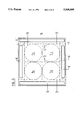
The multiple substrate shown in FIGS. 1 and 2 consists essentially of ceramic layer 1 which is, for example, an aluminum nitride ceramic or an aluminum oxide ceramic and in the embodiment shown is provided with a large number of metal coatings in the form of rectangular metal surfaces 2 on both surface sides. These metal surfaces 2 which consist of copper and are each joined flat to the respective surface side of ceramic layer 1 have each the same shape and size in the embodiment shown and are each made rectangular. Directly opposite each metal surface 2 on one surface side of ceramic layer 1 is metal surface 2 on the other surface side of this ceramic layer. Metal surfaces 2 on one surface side are structured as illustrated in FIG. 1 only for one of metal surface 2 for the sake of simpler representation.
It goes without saying that the metal surfaces can also have a shape deviating from rectangular and/or metal surfaces 2 on each surface side of ceramic layer 1 or on the two surface sides of this ceramic layer can be differently shaped.
There are metal surfaces 2 on the two surface sides of ceramic layer 1 in several rows and in the embodiment shown in a total of three rows R1-R3, of which each has four metal surfaces. Metal surfaces 2 which follow each other in succession in rows R1-R3 and also the metal surfaces of adjacent rows are each spaced at a distance from one another on both surface sides of ceramic layer 1 such that the center lines lie parallel to rows R1-R3 and perpendicular to them between adjacent metal surfaces 2 on one surface side of ceramic layer 1 congruently with the corresponding center lines on the other surface side of this ceramic layer.
Along this center line the ceramic layer on both surface sides is provided with predetermined breaking lines 3 (parallel to rows R1-R3) and with predetermined breaking lines 4 (perpendicularly to rows R1-R3). Ceramic layer 1 is divided into a host of panels 1' by predetermined breaking lines 3 and 4 and other predetermined breaking lines 3'and 4'.
On the border of rectangular ceramic layer 1 in the embodiment shown the layer has on one surface side additional metal coatings in the form of strip- shaped metal surfaces 5 and 6, of which there are metal surfaces 6 each along one border area 1'" of ceramic layer 1 running parallel to predetermined breaking lines 4 and 4' and there are metal surfaces 5 on border area 1" which runs parallel to rows R1-R3 or predetermined breaking lines 3 and 3'. Between these additional, longitudinally stretched out metal coatings 5 and 6 and adjacent metal surfaces 2 or panels 1' there are predetermined breaking lines 3' and 4' on the two surface sides of ceramic layer 1. It goes without saying that predetermined breaking lines 3 and 4 or 3' and 4' are provided on the two surface sides of ceramic layer 1 such that directly opposite one predetermined breaking line 3 or 4 or 3' or 4' on one surface side at a time is a corresponding predetermined breaking line 3 or 4 or 3' or 4' on the other surface side.
In the embodiment shown the additional metal surfaces are dimensioned and arranged such that predetermined breaking lines 3' between metal surfaces 2 and metal surfaces 5 extend as far as the border of ceramic layer 1 by the fact that metal surfaces 5 are each arranged with their narrower sides or ends on a common imaginary line with the long side of metal surfaces 6 which lies outlying, i.e., facing away from metal surfaces 2, however metal surfaces 5 and 6 do not directly adjoin one another, but are spaced at a distance from one another.
Predetermined breaking lines 3' which run between metal surfaces 2 and additional metal surfaces 5 are cut by all predetermined breaking lines 4 and 4'.
With the exception of predetermined breaking lines 3' which run between metal surfaces 2 and additional metal surfaces 5 predetermined breaking lines 3 end on additional metal surfaces 6. In the same way all predetermined breaking lines 4 and 4' end on additional metal surfaces 5.
In the preferred configuration of this embodiment predetermined breaking lines 4 and 4' end on external predetermined breaking lines 3' and predetermined breaking lines 3 end on external predetermined breaking lines 4'.
Basically it is possible to provide additional metal surfaces 5 and 6 on the two surface sides of ceramic layer 1 or only on one surface side.
Metal surfaces 2, 5 and 6 are preferably surfaces of copper.
The described multiple substrate is produced for example by applying to the two surface sides of ceramic layer 1 a metal layer which completely or almost completely covers these surface sides in the form of a metal foil or thin metal plate which is joined flat to the respective surface side of ceramic layer 1 by means of a direct bonding process or active brazing process which are known to one skilled in the art from the literature and which are also called the DCB process (direct copper bonding process) or AMB (active metal brazing process) when using foils or thin plates of copper.
Individual metal surfaces 2, 5 and 6 are then produced by subsequent prestructuring of the continuous metal layers on the two surface sides of ceramic layer 1. This structuring can be done using the most varied processes, for example by etching and/or mechanical processes. After structuring, i.e., after formation of metal surfaces 2, 5 and 6, using suitable techniques predetermined breaking points or predetermined breaking line 3, 4, 3' , 4' are formed, for example, by laser treatment or mechanical processes.
It is also possible to apply predetermined breaking lines 3, 4, 3', and/or 4' before metal coating. By subsequent structuring, preferably by masking and etching, the predetermined breaking lines are then exposed during etching.
Furthermore, it is also possible to join already structured metal surfaces with the ceramic by the DCB process or by the AMB process, predetermined breaking lines 3, 4, 3' and/or 4' being produced either before or after joining the metal surfaces.
In the described prestructured form the multiple substrate is delivered by the substrate manufacturer to the user who then processes this substrate as multiple panels in the production of electrical circuits, especially power circuits, for example, assembled by machine with the required components. Only after this assembly and if necessary after testing of circuits produced is the multiple panel separated into individual circuits by breaking ceramic layer 1 along predetermined breaking lines 3, 4, 3' , and 4'. By means of additional metal surfaces 5 and 6 unwanted breaking of the multiple substrate or multiple panel in the process is effectively prevented. Because predetermined breaking lines 3' which run between metal surfaces 2 and additional metal surfaces 5 extend as far as the border of ceramic layer 1, the multiple panel can be divided into different individual substrates or circuits without the necessity of dividing one of the additional metal surfaces 5 and 6, i.e., when the multiple panel is separated into individual panels or individual substrates or into individual circuits breaking takes place first on the external predetermined breaking lines 3' adjacent to metal surfaces 5 and then on external predetermined breaking lines 4' adjacent to metal surfaces 6, with which then the border which has these additional metal surfaces 5 and 6 is removed and the remaining part of the multiple substrate can then be separated without problems on predetermined breaking lines 3 and 4 by breaking.
Although predetermined breaking lines 3' extend as far as the border of ceramic layer 1 there is no danger that the multiple substrate will break in an unwanted manner during the process along these external predetermined breaking lines 3', since especially when the multiple substrate in the process is always seized during handling on two opposite side borders, no bending forces occur which could cause the substrate to break on outlying predetermined breaking lines 3'. Basically, however, it is also possible to handle the multiple substrate in the process such that this substrate is always seized only on border areas 1"' which have metal surfaces 6.
Metal surfaces 5 and 6 can also be provided with structuring which forms coding, for example, recesses 7 which form coding. This coding which can be read by automatic machinery can then contain information about the type of circuits to be produced and can thus be used to control and/or monitor the production process, but also to securely set a stipulated orientation of the multiple substrate in a processing device.
FIG. 3 shows as another possible embodiment of the invention a multiple substrate which in turn consists of the ceramic layer, metal surfaces on ceramic layer 1 which are not shown in this figure, and additional metal surfaces 5 and 6. Ceramic layer 1 is in turn provided with predetermined breaking lines 3, 4, 3' and 4' which run at right angles to one another. Furthermore, in ceramic layer 1 for this multiple substrate there are short straight predetermined breaking lines 8, of which each ends with one end on predetermined breaking line 3 or 3' and with its other end on predetermined breaking line 4 or 4' and with these predetermined breaking lines encloses an angle less than 90° which opens toward the intersection point of the pertinent predetermined breaking lines 3, 3', 4, or 4', such that the respective panel defined by predetermined breaking lines has the shape of a square or rectangle with beveled corners.
Separation of the multiple substrate according to FIG. 3 into individual panels la takes place in the same manner as was described above for the substrate according to FIG. 1, solely with the difference that at the conclusion breaking takes place along predetermined breaking lines 8. The remnants 9 which arise in this process are discarded.
FIG. 4 shows a multiple substrate in which simply predetermined breaking lines 3', 4, and 4' run in a straight line, instead of predetermined breaking lines 3 zig-zag shaped predetermined breaking lines 3a are provided with an inflection point each on one predetermined breaking line 4, so that these predetermined breaking lines 3a in conjunction with predetermined breaking lines 4 define panels 1b in the shape of a parallelogram. In the same manner as the substrate of FIG. 3 the multiple substrate of FIG. 4 in turn has additional metal surfaces 5 and 6. Division of the multiple substrate into individual panels 1b takes place again by breaking in the manner as was described for the multiple substrate of FIG. 1, however after separation of border areas 1" and 1"' breaking taking place first on predetermined breaking lines 4 so that as the intermediate product several strips are obtained which can then be broken on predetermined breaking lines 3a. The triangular remnants 10 which are formed between external predetermined breaking lines 3' or between border areas 1" and adjacent panels 1b are scrap and are discarded.
FIG. 5 finally shows as another possible version a multiple substrate which is very similar to the multiple substrate of FIG. 3, but which differs from the latter in that instead of short straight predetermined breaking lines 8 arc-shaped predetermined breaking lines 11 are provided and in addition to predetermined breaking lines 3, 4, 3' and 4'. In the version shown in FIG. 5 each four predetermined breaking lines 11 come together to form a circle which is enclosed by predetermined breaking lines 3 and 3' and by two predetermined breaking lines 4 or predetermined breaking lines 4'. Each individual panel is shaped roughly like a round disk in this version.
The invention was described above using examples of embodiments. It goes without saying than numerous changes and modifications are possible without departing from the inventive idea underlying the invention. Thus, for example, it is possible to provide predetermined breaking lines 3, 3a, 4, 3' and/or 4' only on one surface side of ceramic layer 1. Furthermore, it is possible to provide additional metal surfaces 5 and 6 on the two surface sides of ceramic layer 1.
REFERENCE NUMBER LIST
Ceramic layer
1', 1a Panel
1b, 1c Panel
1", 1'" Border area
2 Metal surface
3, 4 Predetermined breaking line
3', 4' Predetermined breaking line
5, 6 Additional metal surface
7 Recess
8 Predetermined breaking line
9, 10 Remnant
11 Predetermined breaking line
R1-R3 Rows

Claims (17)

I claim:
1. A multiple substrate with a ceramic layer comprising:
an array of a plurality of integral adjoining panels, said panels being arranged in at least two adjacent rows on said ceramic layer, with each of said two adjacent rows adjoining an adjacent row in a fixed axial direction (y-axis) which lies in a plane of said ceramic layer and having at least two panels adjoining one another in a second axial direction (x-axis) which lies in said plane of said ceramic layer,
said panels being provided on at least one surface side of said ceramic layer with at least one metal coating,
first predetermined break lines each delineated in said ceramic layer where said at least two panels in said rows adjoin one another,
second predetermined break lines in said ceramic layer between said adjacent rows of panels,
at least one first margin area at a periphery of said ceramic layer having at least one first additional metal surface extending in said second axial direction and bridging all said first predetermined break lines,
said first margin area being defined by a first additional breaking line in said ceramic layer between said at least one first additional metal surface and said array of panels,
at least one second margin area at said periphery of said ceramic layer having at least one additional external metal surface extending in said first axial direction and bridging all said second predetermined break lines, said second margin area being defined by a second additional external break line in said ceramic layer extending in said first axial direction between said at least one second additional metal surface and said array of panels, said at least one first margin area and said at least one second margin area enclosing an angle.
2. A multiple substrate according to claim 1, wherein said external, additional break line of said at least one second margin area is also bridged by said at least one first additional metal surface of said first margin area.
3. A multiple substrate wherein said first predetermined break lines extend in said first direction and said second predetermined break lines extend in said second direction.
4. A multiple substrate according to claim 1, wherein said first and second predetermined break lines intersect at least one external predetermined break line.
5. A multiple substrate according to claim 1, wherein said break lines reach as far as to said at least one external, predetermined break lines.
6. A multiple substrate according to claim 1, wherein said first and second axial directions (x axis, y axis) enclose an angle of 90°.
7. A multiple substrate according to claim 1, wherein said first and second axial directions (x axis, y axis) enclose an angle of less than 90°.
8. A multiple substrate according to claim 1, wherein said external additional break line is also bridged by said at least one additional external metal surface of said second margin area.
9. A multiple substrate according to claim 1 wherein said first and second margin areas enclose an angle of 90°.
10. A multiple substrate according to claim 1, comprising four margins areas, with two first margin areas and two second margin areas being disposed opposite one another on a periphery of said ceramic layer.
11. A multiple substrate according to claim 1, wherein said ceramic layer is scratched on at least one surface side or is provided with groove-shaped depressions to form predetermined breaking lines.
12. A multiple substrate according to claim 1, wherein said at least one first additional metal coating of said at least one first margin area is disposed with margin lines parallel to said first external, additional break line, and wherein said at least one second additional metal surface of said at least one second margin area is disposed with margin lines parallel to said second predetermined external, additional break line.
13. A multiple substrate according to claim 1, wherein said panels have, on both surfaces sides of said ceramic layer at least one metal coating.
14. A multiple substrate according to 1, wherein said at least one margin area has on both surface sides of said ceramic layer, an additional metal surface.
15. A multiple substrate according to claim 1, wherein said at least one metal coating and said additional metal surface of said first and second margin areas are connected flat with said ceramic layer by an active brazing process.
16. A multiple substrate according to claim 6, wherein said first and second axially directions enclose an angle of 90 degrees.
17. A multiple substrate according to claim 1, wherein said at least one metal coating and said additional metal surface of said at least one first and second margin areas are connected flat with said ceramic layer by a direct bonding process.
US08/253,855 1993-06-03 1994-06-03 Multiple substrate and process for its production Expired - Lifetime US5508089A (en)

Priority Applications (1)

Application Number Priority Date Filing Date Title
US08/547,815 US5676855A (en) 1993-06-03 1995-10-25 Multiple substrate and process for its production

Applications Claiming Priority (4)

Application Number Priority Date Filing Date Title
DE4318484 1993-06-03
DE4318484.7 1993-06-03
DE4319944.5 1993-06-16
DE4319944A DE4319944C2 (en) 1993-06-03 1993-06-16 Multiple substrate and process for its manufacture

Related Child Applications (1)

Application Number Title Priority Date Filing Date
US08/547,815 Division US5676855A (en) 1993-06-03 1995-10-25 Multiple substrate and process for its production

Publications (1)

Publication Number Publication Date
US5508089A true US5508089A (en) 1996-04-16

Family

ID=25926470

Family Applications (2)

Application Number Title Priority Date Filing Date
US08/253,855 Expired - Lifetime US5508089A (en) 1993-06-03 1994-06-03 Multiple substrate and process for its production
US08/547,815 Expired - Lifetime US5676855A (en) 1993-06-03 1995-10-25 Multiple substrate and process for its production

Family Applications After (1)

Application Number Title Priority Date Filing Date
US08/547,815 Expired - Lifetime US5676855A (en) 1993-06-03 1995-10-25 Multiple substrate and process for its production

Country Status (3)

Country Link
US (2) US5508089A (en)
EP (1) EP0627760B1 (en)
DE (2) DE4319944C2 (en)

Cited By (13)

* Cited by examiner, † Cited by third party
Publication number Priority date Publication date Assignee Title
US5721044A (en) * 1995-02-09 1998-02-24 Schmidt; Karsten Multiple substrate
US6239381B1 (en) * 1996-04-18 2001-05-29 Kabushiki Kaisha Eastern Circuit board for a semiconductor device and method of making the same
US6638592B1 (en) * 1999-06-14 2003-10-28 Jurgen Schulz-Harder Ceramic/metal substrate, especially composite substrate
US20040018373A1 (en) * 2002-07-29 2004-01-29 Tomoe Suzuki Method for manufacturing printed wiring substrates, metal plate for use in manufacturing printed wiring substrates, and multi-printed wiring-substrate panel
US20050095748A1 (en) * 2001-11-07 2005-05-05 Jurgen Schulz-Harder Method for the selective surface treatment of planar workpieces
US20070007526A1 (en) * 2005-07-08 2007-01-11 Saori Sugiyama Display panel and display device
JP2013033904A (en) * 2011-06-28 2013-02-14 Kyocera Corp Multi-piece wiring board
US20140118981A1 (en) * 2011-06-09 2014-05-01 Otto Bock Healthcare Products Gmbh Method for producing circuit boards and complete circuit board panels
JP2014204031A (en) * 2013-04-08 2014-10-27 三菱マテリアル株式会社 Ceramics original plate for manufacturing power module and multilayer substrate for manufacturing power module
EP3361504A1 (en) * 2017-02-14 2018-08-15 Infineon Technologies AG Power electronic substrate with marker, manufacturing of a power electronic substrate and detection of a marker
JP2019087724A (en) * 2017-11-08 2019-06-06 サムソン エレクトロ−メカニックス カンパニーリミテッド. Substrate strip and electronic device package including the same
CN110379793A (en) * 2019-07-08 2019-10-25 上海申和热磁电子有限公司 One kind covering copper ceramic substrate motherboard structure
US20200006315A1 (en) * 2018-06-27 2020-01-02 Advanced Semiconductor Engineering, Inc. Substrate structure and manufacturing process

Families Citing this family (36)

* Cited by examiner, † Cited by third party
Publication number Priority date Publication date Assignee Title
DE19504378A1 (en) * 1995-02-09 1996-08-14 Curamik Electronics Gmbh Multiple layer ceramic substrate for electronic circuit
DE19615481C5 (en) * 1996-04-03 2013-03-14 Curamik Electronics Gmbh Arched metal-ceramic substrate
EP0862209B1 (en) * 1997-03-01 2009-12-16 Electrovac AG Process for manufacturing a metal-ceramic substrate
US6207221B1 (en) * 1997-03-01 2001-03-27 Jürgen Schulz-Harder Process for producing a metal-ceramic substrate and a metal-ceramic substrate
DE19708363C1 (en) * 1997-03-01 1998-11-05 Schulz Harder Juergen Method of manufacturing a metal-ceramic substrate and metal-ceramic substrate
US5928526A (en) * 1997-04-29 1999-07-27 Stellex Microwave Systems, Inc. Method for manufacturing a substrate having an irregular shape
US6014805A (en) * 1997-10-29 2000-01-18 Lear Automotive Dearborn, Inc. Method of fabricating a hybrid printed circuit board
DE19827414C2 (en) * 1998-06-19 2000-05-31 Schulz Harder Juergen Method of manufacturing a metal-ceramic substrate
US7000316B2 (en) * 1999-09-15 2006-02-21 Curamik Electronics Gmbh Conductor board and method for producing a conductor board
DE10017569C2 (en) * 2000-04-10 2002-11-21 Michael Geringer Device for separating modules from a multiple use having a plurality of such modules
DE10027732A1 (en) * 2000-06-03 2001-12-06 Kem Tec Service Gmbh Multiple use circuit board provided on both sides with rupture lines using displacement of circuit board relative to opposing laser beam elements
DE10040450B4 (en) 2000-08-18 2008-07-10 Osram Opto Semiconductors Gmbh Semiconductor laser device with a cooling element
DE10158185B4 (en) * 2000-12-20 2005-08-11 Semikron Elektronik Gmbh Power semiconductor module with high insulation resistance
DE10063714C2 (en) * 2000-12-20 2002-11-07 Semikron Elektronik Gmbh Power semiconductor module with high insulation strength
AU2003222722A1 (en) * 2002-03-13 2003-09-29 Jurgen Schulz-Harder Method for the production of a metal-ceramic substrate, preferably a copper-ceramic substrate
DE10212495B4 (en) 2002-03-21 2004-02-26 Schulz-Harder, Jürgen, Dr.-Ing. Method for producing a metal-ceramic substrate, preferably a copper-ceramic substrate
DE102004014438A1 (en) * 2004-03-24 2005-11-03 Siemens Ag Circuit board benefits with a variety of circuit carriers, circuit carrier and method for separating circuit carriers from a circuit board benefits
DE102004022430A1 (en) * 2004-05-06 2005-12-01 Siemens Ag Method for mechanically separating circuit carriers from a circuit board benefit
KR101534124B1 (en) * 2007-04-25 2015-07-06 세람테크 게엠베하 Chip resistor substrate
DE102012110382B4 (en) 2011-12-21 2021-02-18 Rogers Germany Gmbh Substrate and method for manufacturing a substrate
DE102012212131A1 (en) * 2012-07-11 2014-06-26 Semikron Elektronik Gmbh & Co. Kg Substrate and method for fracture preparation of a substrate for at least one power semiconductor device
DE102013105528B4 (en) * 2013-05-29 2021-09-02 Rogers Germany Gmbh Metal-ceramic substrate and a method for producing a metal-ceramic substrate
DE202016008287U1 (en) 2016-02-26 2017-06-21 Heraeus Deutschland GmbH & Co. KG Copper-ceramic composite
HUE053117T2 (en) 2016-02-26 2021-06-28 Heraeus Deutschland Gmbh & Co Kg Copper-ceramic composites
DE202016008371U1 (en) 2016-02-26 2017-09-11 Heraeus Deutschland GmbH & Co. KG Copper-ceramic composite
DE102016203112B4 (en) 2016-02-26 2019-08-29 Heraeus Deutschland GmbH & Co. KG Copper-ceramic composite
WO2017144332A1 (en) 2016-02-26 2017-08-31 Heraeus Deutschland GmbH & Co. KG Copper-ceramic composite
DE202016008370U1 (en) 2016-02-26 2017-09-11 Heraeus Deutschland GmbH & Co. KG Copper-ceramic composite
DE102016203058B3 (en) 2016-02-26 2017-05-18 Heraeus Deutschland GmbH & Co. KG Copper-ceramic composite and module
EP3210957B1 (en) 2016-02-26 2019-01-02 Heraeus Deutschland GmbH & Co. KG Copper ceramic composite
DE202016008307U1 (en) 2016-02-26 2017-07-10 Heraeus Deutschland GmbH & Co. KG Copper-ceramic composite
DE202016008286U1 (en) 2016-02-26 2017-06-21 Heraeus Deutschland GmbH & Co. KG Copper-ceramic composite
EP3210956B1 (en) 2016-02-26 2018-04-11 Heraeus Deutschland GmbH & Co. KG Copper ceramic composite
DE102016203030B4 (en) 2016-02-26 2025-05-08 Heraeus Electronics Gmbh & Co. Kg Copper-ceramic composite and a module containing this composite
EP3217428B1 (en) * 2016-03-07 2022-09-07 Infineon Technologies AG Multiple substrate and method for the production of same
DE102021122633B4 (en) 2021-09-01 2025-10-16 Semikron Elektronik Gmbh & Co. Kg Substrate for a power electronic circuit

Citations (5)

* Cited by examiner, † Cited by third party
Publication number Priority date Publication date Assignee Title
EP0149923A2 (en) * 1984-01-23 1985-07-31 The Jade Corporation Microcircuit substrate and method of making same
DE3906690A1 (en) * 1989-03-02 1989-10-12 Siemens Ag CERAMIC PLATE FOR PERFORMANCE SEMICONDUCTOR MODULES
DE3931996A1 (en) * 1988-09-30 1990-04-05 Marconi Electronic Devices SEMICONDUCTOR DEVICE AND METHOD FOR THE PRODUCTION THEREOF
DE3939794A1 (en) * 1989-12-01 1991-06-06 Semikron Elektronik Gmbh CARRIER PLATE FOR SEMICONDUCTOR CONSTRUCTION UNITS
US5047279A (en) * 1989-01-26 1991-09-10 Shin-Kobe Electric Machinery Company, Ltd. Multilayer printed circuit board

Family Cites Families (8)

* Cited by examiner, † Cited by third party
Publication number Priority date Publication date Assignee Title
GB1315479A (en) * 1970-06-24 1973-05-02 Licentia Gmbh Method for manufacturing diodes
DE2213115C3 (en) * 1972-03-17 1975-12-04 Siemens Ag, 1000 Berlin Und 8000 Muenchen Process for the high-strength joining of ceramics made of carbides, including diamonds, borides, nitrides or suicides, with metal by the dry soldering process
US3926746A (en) * 1973-10-04 1975-12-16 Minnesota Mining & Mfg Electrical interconnection for metallized ceramic arrays
US3997964A (en) * 1974-09-30 1976-12-21 General Electric Company Premature breakage resistant semiconductor wafer and method for the manufacture thereof
US3994430A (en) * 1975-07-30 1976-11-30 General Electric Company Direct bonding of metals to ceramics and metals
JPS55124243A (en) * 1979-03-20 1980-09-25 Nec Corp Compound semiconductor device
US4922326A (en) * 1988-07-18 1990-05-01 Motorola, Inc. Ceramic semiconductor package having crack arrestor patterns
JPH07120646B2 (en) * 1990-05-16 1995-12-20 株式会社東芝 Method for manufacturing mesa type semiconductor pellets

Patent Citations (5)

* Cited by examiner, † Cited by third party
Publication number Priority date Publication date Assignee Title
EP0149923A2 (en) * 1984-01-23 1985-07-31 The Jade Corporation Microcircuit substrate and method of making same
DE3931996A1 (en) * 1988-09-30 1990-04-05 Marconi Electronic Devices SEMICONDUCTOR DEVICE AND METHOD FOR THE PRODUCTION THEREOF
US5047279A (en) * 1989-01-26 1991-09-10 Shin-Kobe Electric Machinery Company, Ltd. Multilayer printed circuit board
DE3906690A1 (en) * 1989-03-02 1989-10-12 Siemens Ag CERAMIC PLATE FOR PERFORMANCE SEMICONDUCTOR MODULES
DE3939794A1 (en) * 1989-12-01 1991-06-06 Semikron Elektronik Gmbh CARRIER PLATE FOR SEMICONDUCTOR CONSTRUCTION UNITS

Non-Patent Citations (1)

* Cited by examiner, † Cited by third party
Title
Break Apart Laminated Substrates by W. J. Gyurk Technical Digest No. 4. Oct. 1966. *

Cited By (21)

* Cited by examiner, † Cited by third party
Publication number Priority date Publication date Assignee Title
US5721044A (en) * 1995-02-09 1998-02-24 Schmidt; Karsten Multiple substrate
US6239381B1 (en) * 1996-04-18 2001-05-29 Kabushiki Kaisha Eastern Circuit board for a semiconductor device and method of making the same
US6638592B1 (en) * 1999-06-14 2003-10-28 Jurgen Schulz-Harder Ceramic/metal substrate, especially composite substrate
US20050095748A1 (en) * 2001-11-07 2005-05-05 Jurgen Schulz-Harder Method for the selective surface treatment of planar workpieces
CN1301636C (en) * 2002-07-29 2007-02-21 日本特殊陶业株式会社 Method for manufacturing printed wiring substrates, metal plate for use in manufacturing printed wiring substrates, and multi-printed wiring-substrate panel
US20040018373A1 (en) * 2002-07-29 2004-01-29 Tomoe Suzuki Method for manufacturing printed wiring substrates, metal plate for use in manufacturing printed wiring substrates, and multi-printed wiring-substrate panel
US6872436B2 (en) * 2002-07-29 2005-03-29 Ngk Spark Plug Co. Ltd. Method for manufacturing printed wiring substrates, metal plate for use in manufacturing printed wiring substrates, and multi-printed wiring-substrate panel
US20050155789A1 (en) * 2002-07-29 2005-07-21 Ngk Spark Plug Co., Ltd. Method for manufacturing printed wiring substrates, metal plate for use in manufacturing printed wiring substrates, and multi-printed wiring-substrate panel
US6976415B2 (en) 2002-07-29 2005-12-20 Ngk Spark Plug Co., Ltd. Method for manufacturing printed wiring substrates, metal plate for use in manufacturing printed wiring substrates, and multi-printed wiring-substrate panel
US7719650B2 (en) * 2005-07-08 2010-05-18 Hitachi Displays, Ltd. Display panel and display device
US20070007526A1 (en) * 2005-07-08 2007-01-11 Saori Sugiyama Display panel and display device
US20140118981A1 (en) * 2011-06-09 2014-05-01 Otto Bock Healthcare Products Gmbh Method for producing circuit boards and complete circuit board panels
US9386710B2 (en) * 2011-06-09 2016-07-05 Otto Bock Healthcare Products Gmbh Method for producing circuit boards and complete circuit board panels
JP2013033904A (en) * 2011-06-28 2013-02-14 Kyocera Corp Multi-piece wiring board
JP2014204031A (en) * 2013-04-08 2014-10-27 三菱マテリアル株式会社 Ceramics original plate for manufacturing power module and multilayer substrate for manufacturing power module
EP3361504A1 (en) * 2017-02-14 2018-08-15 Infineon Technologies AG Power electronic substrate with marker, manufacturing of a power electronic substrate and detection of a marker
JP2019087724A (en) * 2017-11-08 2019-06-06 サムソン エレクトロ−メカニックス カンパニーリミテッド. Substrate strip and electronic device package including the same
JP7087241B2 (en) 2017-11-08 2022-06-21 サムソン エレクトロ-メカニックス カンパニーリミテッド. Substrate strip and electronic device package including it
US20200006315A1 (en) * 2018-06-27 2020-01-02 Advanced Semiconductor Engineering, Inc. Substrate structure and manufacturing process
US11189610B2 (en) * 2018-06-27 2021-11-30 Advanced Semiconductor Engineering, Inc. Substrate structure and manufacturing process
CN110379793A (en) * 2019-07-08 2019-10-25 上海申和热磁电子有限公司 One kind covering copper ceramic substrate motherboard structure

Also Published As

Publication number Publication date
EP0627760B1 (en) 1999-09-08
DE59408709D1 (en) 1999-10-14
DE4319944A1 (en) 1994-12-08
EP0627760A1 (en) 1994-12-07
US5676855A (en) 1997-10-14
DE4319944C2 (en) 1998-07-23

Similar Documents

Publication Publication Date Title
US5508089A (en) Multiple substrate and process for its production
US4797715A (en) Optoelectric component for surface mounting
US6276995B1 (en) Electronic component and method of manufacturing same
US4289384A (en) Electrode structures and interconnecting system
US6727111B2 (en) Process for making electronic chip device incorporating plural elements
US5721044A (en) Multiple substrate
EP0442491B1 (en) Semiconductor device having a wiring pattern in which a plurality of lines are arranged in close proximity to one another
JP2001044141A (en) Method for cutting semiconductor substrate
JP3211609B2 (en) Multilayer electronic component and method of manufacturing the same
KR100200687B1 (en) Semiconductor device with new pad layer
JPH0354876A (en) Laminated displacement element
JPH05145209A (en) Terminal connection structure
JPH02187305A (en) Wafer dividing blade
JPH0220046A (en) Enamel board and manufacture thereof
JPH03283637A (en) Semiconductor device
EP0262830A2 (en) Method of ensuring contact in a deposited layer
JPH03159153A (en) How to divide a semiconductor substrate
JPS58166725A (en) Forming method for opening section of laminated coating layer
EP0603973A2 (en) Method of manufacturing a semiconductor device provided with a number of pn junctions separated each time by depression, and semiconductor device provided with a number of pn junctions separated each time by a depression.
EP0225333B1 (en) Mini chip carrier slotted array
JPH04124893A (en) ceramic substrate
JPS62123745A (en) Ceramic package type semiconductor device
JPH06260746A (en) Solder connection structure
JPH06310862A (en) Ceramic multilayered circuit board with cavity
JPH07326830A (en) Surface mount device and its manufacture

Legal Events

Date Code Title Description
STCF Information on status: patent grant

Free format text: PATENTED CASE

FEPP Fee payment procedure

Free format text: PAYOR NUMBER ASSIGNED (ORIGINAL EVENT CODE: ASPN); ENTITY STATUS OF PATENT OWNER: LARGE ENTITY

FPAY Fee payment

Year of fee payment: 4

FPAY Fee payment

Year of fee payment: 8

AS Assignment

Owner name: ELECTROVA AG, AUSTRIA

Free format text: ASSIGNMENT OF ASSIGNORS INTEREST;ASSIGNOR:SCHULZ-HARDER, JURGEN;REEL/FRAME:017125/0926

Effective date: 20051118

FPAY Fee payment

Year of fee payment: 12

REMI Maintenance fee reminder mailed
AS Assignment

Owner name: CURAMIK HOLDING GMBH, IN LIQUIDATION, GERMANY

Free format text: CHANGE OF NAME;ASSIGNOR:ELECTROVAC AG;REEL/FRAME:026015/0157

Effective date: 20110218

Owner name: CURAMIK ELECTRONICS GMBH, GERMANY

Free format text: ASSIGNMENT OF ASSIGNORS INTEREST;ASSIGNOR:CURAMIK HOLDING GMBH IN LIQUIDATION;REEL/FRAME:026015/0375

Effective date: 20110131

FEPP Fee payment procedure

Free format text: PAT HOLDER NO LONGER CLAIMS SMALL ENTITY STATUS, ENTITY STATUS SET TO UNDISCOUNTED (ORIGINAL EVENT CODE: STOL); ENTITY STATUS OF PATENT OWNER: LARGE ENTITY

SULP Surcharge for late payment