US5500103A - Method for preparing thin film electro-luminescence element - Google Patents
Method for preparing thin film electro-luminescence element Download PDFInfo
- Publication number
- US5500103A US5500103A US08/452,729 US45272995A US5500103A US 5500103 A US5500103 A US 5500103A US 45272995 A US45272995 A US 45272995A US 5500103 A US5500103 A US 5500103A
- Authority
- US
- United States
- Prior art keywords
- target
- light
- emitting layer
- film
- doping material
- Prior art date
- Legal status (The legal status is an assumption and is not a legal conclusion. Google has not performed a legal analysis and makes no representation as to the accuracy of the status listed.)
- Expired - Fee Related
Links
Images


Classifications
-
- H—ELECTRICITY
- H05—ELECTRIC TECHNIQUES NOT OTHERWISE PROVIDED FOR
- H05B—ELECTRIC HEATING; ELECTRIC LIGHT SOURCES NOT OTHERWISE PROVIDED FOR; CIRCUIT ARRANGEMENTS FOR ELECTRIC LIGHT SOURCES, IN GENERAL
- H05B33/00—Electroluminescent light sources
- H05B33/10—Apparatus or processes specially adapted to the manufacture of electroluminescent light sources
-
- C—CHEMISTRY; METALLURGY
- C09—DYES; PAINTS; POLISHES; NATURAL RESINS; ADHESIVES; COMPOSITIONS NOT OTHERWISE PROVIDED FOR; APPLICATIONS OF MATERIALS NOT OTHERWISE PROVIDED FOR
- C09K—MATERIALS FOR MISCELLANEOUS APPLICATIONS, NOT PROVIDED FOR ELSEWHERE
- C09K11/00—Luminescent, e.g. electroluminescent, chemiluminescent materials
- C09K11/08—Luminescent, e.g. electroluminescent, chemiluminescent materials containing inorganic luminescent materials
- C09K11/57—Luminescent, e.g. electroluminescent, chemiluminescent materials containing inorganic luminescent materials containing manganese or rhenium
- C09K11/572—Chalcogenides
- C09K11/574—Chalcogenides with zinc or cadmium
-
- C—CHEMISTRY; METALLURGY
- C23—COATING METALLIC MATERIAL; COATING MATERIAL WITH METALLIC MATERIAL; CHEMICAL SURFACE TREATMENT; DIFFUSION TREATMENT OF METALLIC MATERIAL; COATING BY VACUUM EVAPORATION, BY SPUTTERING, BY ION IMPLANTATION OR BY CHEMICAL VAPOUR DEPOSITION, IN GENERAL; INHIBITING CORROSION OF METALLIC MATERIAL OR INCRUSTATION IN GENERAL
- C23C—COATING METALLIC MATERIAL; COATING MATERIAL WITH METALLIC MATERIAL; SURFACE TREATMENT OF METALLIC MATERIAL BY DIFFUSION INTO THE SURFACE, BY CHEMICAL CONVERSION OR SUBSTITUTION; COATING BY VACUUM EVAPORATION, BY SPUTTERING, BY ION IMPLANTATION OR BY CHEMICAL VAPOUR DEPOSITION, IN GENERAL
- C23C14/00—Coating by vacuum evaporation, by sputtering or by ion implantation of the coating forming material
- C23C14/0021—Reactive sputtering or evaporation
- C23C14/0036—Reactive sputtering
- C23C14/0057—Reactive sputtering using reactive gases other than O2, H2O, N2, NH3 or CH4
-
- C—CHEMISTRY; METALLURGY
- C23—COATING METALLIC MATERIAL; COATING MATERIAL WITH METALLIC MATERIAL; CHEMICAL SURFACE TREATMENT; DIFFUSION TREATMENT OF METALLIC MATERIAL; COATING BY VACUUM EVAPORATION, BY SPUTTERING, BY ION IMPLANTATION OR BY CHEMICAL VAPOUR DEPOSITION, IN GENERAL; INHIBITING CORROSION OF METALLIC MATERIAL OR INCRUSTATION IN GENERAL
- C23C—COATING METALLIC MATERIAL; COATING MATERIAL WITH METALLIC MATERIAL; SURFACE TREATMENT OF METALLIC MATERIAL BY DIFFUSION INTO THE SURFACE, BY CHEMICAL CONVERSION OR SUBSTITUTION; COATING BY VACUUM EVAPORATION, BY SPUTTERING, BY ION IMPLANTATION OR BY CHEMICAL VAPOUR DEPOSITION, IN GENERAL
- C23C14/00—Coating by vacuum evaporation, by sputtering or by ion implantation of the coating forming material
- C23C14/06—Coating by vacuum evaporation, by sputtering or by ion implantation of the coating forming material characterised by the coating material
- C23C14/0623—Sulfides, selenides or tellurides
- C23C14/0629—Sulfides, selenides or tellurides of zinc, cadmium or mercury
-
- H—ELECTRICITY
- H05—ELECTRIC TECHNIQUES NOT OTHERWISE PROVIDED FOR
- H05B—ELECTRIC HEATING; ELECTRIC LIGHT SOURCES NOT OTHERWISE PROVIDED FOR; CIRCUIT ARRANGEMENTS FOR ELECTRIC LIGHT SOURCES, IN GENERAL
- H05B33/00—Electroluminescent light sources
- H05B33/12—Light sources with substantially two-dimensional radiating surfaces
- H05B33/14—Light sources with substantially two-dimensional radiating surfaces characterised by the chemical or physical composition or the arrangement of the electroluminescent material, or by the simultaneous addition of the electroluminescent material in or onto the light source
Definitions
- the present invention relates to a method for preparing a thin-film EL (Electro-luminescence) element, a light emitting layer of which is formed by sputtering.
- FIG. 2 is a cross-sectional drawing of a conventional thin-film EL element.
- the thin film EL element has a double insulating structure, wherein a transparent electrode 12, first insulating layer 13, EL light-emitting layer 14, second insulating layer 15, and back electrode 16 are all prepared on a glass substrate 11.
- the light-emitting layer 14 is made of II-VI group element sulfide, to which doping material yielding luminescent centers such as a small quantity of Mn, Tb, Sm, Tm, Pr, etc. are added thereto.
- the II-VI group element sulfide utilized may include zinc sulfide (ZnS), calcium sulfide (CaS), strontium sulfide (SrS), and others.
- the vacuum evaporation method the atomic layer crystal growth evaporation (ALE) method, which is one of the CVD methods
- the sputtering method Since the sputtering method can prepare a uniform film having a large area, it is most suitable for mass production.
- Light-emitting layers prepared by the sputtering method are inferior in light-emitting luminance (See ACTA POLYTECNICA SCANDINAVICA, Applied Physics Series, No.170 "5th International Work Shop on Electrochemistry” pp. 41-48). Further examination of the sputtering method by applicants has shown that zinc, manganese, and sulfur are different from one another in physical properties such as sputter rate and vapor pressure: that actual film composition is considerably different from target composition; and that the crystalline nature of the light-emitting layer is degraded as a result.
- Reactive sputtering is expected to be a method for obtaining a uniform and high quality light-emitting layer.
- Japanese laid-open application No. 62-271396 discloses a reactive sputtering method using a zinc target and hydrogen sulfide gas.
- a uniform and high quality light-emitting layer is prepared by using an inactive gas containing 5-20% hydrogen sulfide (H 2 S) by volume and by setting substrate temperature to 100°-350° C.
- H 2 S hydrogen sulfide
- a particularly good result is obtained when the substrate temperature is set to a range of 200°-250° C., the hydrogen sulfide concentration is set to 10%, the electric discharge pressure is set to 10 mTorr, and the electric discharge power is set to 8 W/in 2 (1.2 W/cm 2 ).
- a light-emitting layer produced under the above conditions has a film-forming rate of about 13 nm/min, which is too slow for practical use. While a high film-forming rate can be achieved by using a high electric discharge power, a light-emitting layer having good characteristics cannot be obtained simply by increasing electric discharge power. Increasing electric discharge alone increases only the quantity of zinc and manganese supplied; the supply of sulfur does not keep balance with the supply of zinc or manganese. As a consequence, the composite ratio of zinc to sulfur in the film is no longer 1 to 1, and a light-emitting layer having good characteristics cannot be obtained.
- the present invention is designed to optimize the reactive sputtering method and to provide a method for preparing a light-emitting layer superior in film formation rate and film quality for which the film is kept to have a stoichiometric composition giving good light-emitting characteristics.
- the present invention uses the following method to surmount the limitations of the prior art for preparing a thin-film EL element.
- the present invention is a method for preparing a thin-film EL element that includes a light-emitting layer consisting of zinc sulfide to which a doping material yielding a luminescent center is added.
- a sputtering gas containing hydrogen sulfide gas at greater than 20% in volume in inactive gas is used; based on the hydrogen sulfide concentration, an optimal electric discharge is applied to sputter a target.
- targets made of an alloy of zinc and a doping material yielding luminescent centers are used. More specifically, either of the following is used: a zinc target to which a doping material yielding a luminescent center plate with area in a prescribed ratio to the exposed area of zinc is made to adhere, or both of target consisting of a zinc and consisting of doping material yielding luminescent centers are used. Manganese is used as a luminescent center material. Then, sputtering gas containing hydrogen sulfide at a concentration of 25% to 50% in volume is applied, and supplying the target with electric discharge power at a density of 2 to 5 W/cm 2 .
- FIG. 3 is a block diagram showing the relationship between electric discharge power and light-emitting luminance, using H 2 S concentration as parameter.
- a target with a diameter of 100 mm was used.
- an optimal value of electric discharge power can be determined.
- the optimal electric discharge power for the given concentration of H 2 S generates a high quality light-emitting layer.
- FIG. 1 is a cross-sectional drawing showing a sputtering apparatus relating to an embodiment of the present invention
- FIG. 2 is a cross-sectional drawing showing a thin-film EL element that is prepared in accordance with the embodiment of the present invention
- FIG. 3 is a diagram showing the relationship between electric discharge power and light-emitting luminance, using H 2 S concentration as a parameter
- FIG. 4 is a cross-sectional view showing a sputtering apparatus relating to another embodiment of the present invention.
- FIG. 2 is a cross-sectional view showing a thin-film EL element relating to an embodiment of the present invention.
- a transparent electrode 12 with a thickness of 1700 ⁇ is prepared on glass substrate 11 by sputtering an ITO target.
- the first insulating layer 13 consists of a tantalum pent-oxide (Ta 2 O 5 ) layer and a silicon dioxide (SiO 2 ) layer, wherein the tantalum pentoxide (Ta 2 O 5 ) layer is prepared on the silicon dioxide (SiO 2 ) at a thickness ratio of 1:9. Since Ta 2 O 5 has a large dielectric constant, the voltage applied to the insulating layer when the thin-film EL element is driven is reduced, thereby lowing the applied driving voltage. The tantalum pentoxide Ta 2 O 5 that is made to adhere directly on to the ITO film loses the characteristics of the ITO film. Accordingly, the SiO 2 film is provided between the (Ta 2 O 5 ) layer and the ITO film.
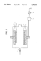
- FIG. 1 is a cross-sectional view of the sputtering apparatus relating to an embodiment of the present invention.
- reactive chamber 1 negative electrode 3, to which target 2 is made to adhere, is positioned opposite from positive electrode 4, in which substrate 11 is installed.
- Transparent electrode 12 and the first insulating layer 13 are laminated on substrate 11.
- Negative electrode 3 is connected to a 13.56 MHz RF power supply 6 via matching circuit 5.
- Positive electrode 4 is grounded.
- Target 2 has a 100 mm zinc manganese alloy disc including 0.5 wt % manganese.
- the sputtering gas is argon gas (Ar) containing H 2 S at a volume ratio of 40%. Mixed gas is supplied to reactive chamber 1 from gas inlet port 7 at a flow rate of 40 sccm.
- Light emitting layer 14 with a thickness of 0.7 um was prepared under a gas pressure of 10 mTorr, a substrate temperature of 350° C., and an electric discharge power density of 3.8 W/cm 2 . Under these conditions, a film forming rate as high as 70 nm/min could be obtained. A similar formation rate was obtained when a gas pressure ranging from 5-20 mTorr was used and a gas flow rate ranging from 10-60 sccm was used. The film thickness of the light-emitting layer 14 is adjusted in a range of 0.6-1.0 um. As line B in FIG. 3 shows, an electric discharge density of 3.8 W/cm 2 corresponds to electric discharge power at a peak value of 300 W.
- the second insulating layer 15 is prepared.
- the second insulating layer 15 is made to adhere firmly to the light-emitting layer 14 via the SiO 2 .
- back electrode 16 is prepared.
- Back electrode 16 consists of Al film and Ni film at a thickness ratio of 1:1. Insulating layer 15 is made to adhere firmly to the Ni film via the Al film of back electrode 16. Ni provides good solderability.
- the thin-film EL element thus obtained produces a light-emitting luminance as high as 250 cd/m 2 .
- a mosaic target consists of a Zn target and a manganese plate which is made to adhere to the Zn target; the area ratio of the Zn target to the manganese plate corresponds to their composition ratio.
- FIG. 4 is a layout view showing the sputtering apparatus relating to another embodiment of the present invention. This sputtering apparatus is driven using a co-sputtering method. Components in FIG. 4 common to those in FIG. 1 are represented with the same reference numbers.
- Positive electrode 4 is connected to rotary mechanism 8.
- the negative electrode consists of two negative electrodes 31 and 32, each of which is connected to an RF power supply 6 via matching circuit 5.
- Zn target 21 is laid on negative electrode 31, and Mn target 22 on negative electrode 32.
- Light-emitting layer 4 containing manganese of 0.5 wt % was formed at a gas pressure of 10 mTorr and substrate temperature of 350° C. Positive electrode 4 rotates at 50 rpm.
- An electric discharge power of 3.8 W/cm 2 is applied to the Zn target on the negative electrode 21, and 0.5 W/cm 2 electric discharge power is applied to the Mn target on the negative electrode 22.
- the film was formed at a rate of about 70 nm/min.
- the resulting thin-film EL element showed a high light-emitting luminance, similar to the aforementioned embodiment.
- the ratio of electric discharge power applied to targets 21 to electric discharge power applied to target 22 is adjusted so that the Mn concentration in the light-emitting layer is maintained and controlled at the optimal value.
- a thin-film EL element was produced in which a transparent electrode ITO with a thickness of 1700 ⁇ , first insulating layer of silicon dioxide and silicon nitride with a thickness of 2100 ⁇ , a light-emitting layer with a thickness of 7000 ⁇ , a second insulating layer of silicon dioxide and silicon nitride with a thickness of 2100 ⁇ , and a back electrode of aluminum with a thickness of 7000 ⁇ are sequentially formed.
- a Zn--Mn alloy target was used to form the light-emitting layer.
- the concentration of the manganese used was 0.3 wt %.
- the sputtering gas used was argon gas to which hydrogen sulfide gas had been added at a prescribed concentration.
- the sputtering was executed at a gas pressure of 10 mTorr and a substrate temperature of 400° C. Table 1 shows the film-forming conditions and rate.
- the surface of the Zn--Mn alloy target is sulfurized under the aforementioned condition.
- the light-emitting layer is heated at 500° C. after the film is formed.
- the light-emitting luminance of the obtained thin-film EL element is high.
- Table 1 indicates that the light-emitting layer is formed three to seven times faster using the method of the present invention than by the conventional method.
- a thin-film EL element is prepared by using sputtering gas containing hydrogen sulfide with a concentration by volume of greater than 20%, and by applying appropriate electric discharge power to the hydrogen sulfide concentration contained in the sputtering gas to sputter a Mn--Zn alloy target, a mosaic target, or manganese and zinc targets individually.
- a high-quality light-emitting layer is prepared at a sufficiently practical film-formation speed three to seven times that obtained using the prior art.
Landscapes
- Chemical & Material Sciences (AREA)
- Engineering & Computer Science (AREA)
- Materials Engineering (AREA)
- Organic Chemistry (AREA)
- Chemical Kinetics & Catalysis (AREA)
- Mechanical Engineering (AREA)
- Metallurgy (AREA)
- Manufacturing & Machinery (AREA)
- Inorganic Chemistry (AREA)
- Electroluminescent Light Sources (AREA)
Abstract
A light-emitting layer is prepared by using sputtering gas containing H2 S gas at a concentration greater than 20% by volume, and by sputtering a target under the optimal electric discharge power corresponding to the concentration of H2 S gas. A light-emitting layer having good light-emitting characteristics is obtained under a high film-forming rate.
Description
This is a Continuation of application Ser. No. 08/161,490 filed Dec. 6, 1993, now abandoned.
The present invention relates to a method for preparing a thin-film EL (Electro-luminescence) element, a light emitting layer of which is formed by sputtering.
FIG. 2 is a cross-sectional drawing of a conventional thin-film EL element. The thin film EL element has a double insulating structure, wherein a transparent electrode 12, first insulating layer 13, EL light-emitting layer 14, second insulating layer 15, and back electrode 16 are all prepared on a glass substrate 11. The light-emitting layer 14 is made of II-VI group element sulfide, to which doping material yielding luminescent centers such as a small quantity of Mn, Tb, Sm, Tm, Pr, etc. are added thereto. The II-VI group element sulfide utilized may include zinc sulfide (ZnS), calcium sulfide (CaS), strontium sulfide (SrS), and others.
Several different methods have been examined for preparing the light-emitting layer, including the vacuum evaporation method, the atomic layer crystal growth evaporation (ALE) method, which is one of the CVD methods, and the sputtering method. Since the sputtering method can prepare a uniform film having a large area, it is most suitable for mass production.
Light-emitting layers prepared by the sputtering method, however, are inferior in light-emitting luminance (See ACTA POLYTECNICA SCANDINAVICA, Applied Physics Series, No.170 "5th International Work Shop on Electrochemistry" pp. 41-48). Further examination of the sputtering method by applicants has shown that zinc, manganese, and sulfur are different from one another in physical properties such as sputter rate and vapor pressure: that actual film composition is considerably different from target composition; and that the crystalline nature of the light-emitting layer is degraded as a result.
Reactive sputtering is expected to be a method for obtaining a uniform and high quality light-emitting layer. Japanese laid-open application No. 62-271396 discloses a reactive sputtering method using a zinc target and hydrogen sulfide gas. A uniform and high quality light-emitting layer is prepared by using an inactive gas containing 5-20% hydrogen sulfide (H2 S) by volume and by setting substrate temperature to 100°-350° C. A particularly good result is obtained when the substrate temperature is set to a range of 200°-250° C., the hydrogen sulfide concentration is set to 10%, the electric discharge pressure is set to 10 mTorr, and the electric discharge power is set to 8 W/in2 (1.2 W/cm2).
A light-emitting layer produced under the above conditions, however, has a film-forming rate of about 13 nm/min, which is too slow for practical use. While a high film-forming rate can be achieved by using a high electric discharge power, a light-emitting layer having good characteristics cannot be obtained simply by increasing electric discharge power. Increasing electric discharge alone increases only the quantity of zinc and manganese supplied; the supply of sulfur does not keep balance with the supply of zinc or manganese. As a consequence, the composite ratio of zinc to sulfur in the film is no longer 1 to 1, and a light-emitting layer having good characteristics cannot be obtained.
The present invention is designed to optimize the reactive sputtering method and to provide a method for preparing a light-emitting layer superior in film formation rate and film quality for which the film is kept to have a stoichiometric composition giving good light-emitting characteristics.
The present invention uses the following method to surmount the limitations of the prior art for preparing a thin-film EL element. Specifically, the present invention is a method for preparing a thin-film EL element that includes a light-emitting layer consisting of zinc sulfide to which a doping material yielding a luminescent center is added. In this method, a sputtering gas containing hydrogen sulfide gas at greater than 20% in volume in inactive gas is used; based on the hydrogen sulfide concentration, an optimal electric discharge is applied to sputter a target.
Further, in the present invention, targets made of an alloy of zinc and a doping material yielding luminescent centers are used. More specifically, either of the following is used: a zinc target to which a doping material yielding a luminescent center plate with area in a prescribed ratio to the exposed area of zinc is made to adhere, or both of target consisting of a zinc and consisting of doping material yielding luminescent centers are used. Manganese is used as a luminescent center material. Then, sputtering gas containing hydrogen sulfide at a concentration of 25% to 50% in volume is applied, and supplying the target with electric discharge power at a density of 2 to 5 W/cm2.
FIG. 3 is a block diagram showing the relationship between electric discharge power and light-emitting luminance, using H2 S concentration as parameter. A target with a diameter of 100 mm was used. When the concentration of H2 S gas contained in the sputtering gas is constant, an optimal value of electric discharge power can be determined. The optimal electric discharge power for the given concentration of H2 S generates a high quality light-emitting layer.
FIG. 1 is a cross-sectional drawing showing a sputtering apparatus relating to an embodiment of the present invention;
FIG. 2 is a cross-sectional drawing showing a thin-film EL element that is prepared in accordance with the embodiment of the present invention;
FIG. 3 is a diagram showing the relationship between electric discharge power and light-emitting luminance, using H2 S concentration as a parameter; and
FIG. 4 is a cross-sectional view showing a sputtering apparatus relating to another embodiment of the present invention.
FIG. 2 is a cross-sectional view showing a thin-film EL element relating to an embodiment of the present invention. A transparent electrode 12 with a thickness of 1700 Å is prepared on glass substrate 11 by sputtering an ITO target. The first insulating layer 13 consists of a tantalum pent-oxide (Ta2 O5) layer and a silicon dioxide (SiO2) layer, wherein the tantalum pentoxide (Ta2 O5) layer is prepared on the silicon dioxide (SiO2) at a thickness ratio of 1:9. Since Ta2 O5 has a large dielectric constant, the voltage applied to the insulating layer when the thin-film EL element is driven is reduced, thereby lowing the applied driving voltage. The tantalum pentoxide Ta2 O5 that is made to adhere directly on to the ITO film loses the characteristics of the ITO film. Accordingly, the SiO2 film is provided between the (Ta2 O5) layer and the ITO film.
FIG. 1 is a cross-sectional view of the sputtering apparatus relating to an embodiment of the present invention. In reactive chamber 1, negative electrode 3, to which target 2 is made to adhere, is positioned opposite from positive electrode 4, in which substrate 11 is installed. Transparent electrode 12 and the first insulating layer 13 are laminated on substrate 11. Negative electrode 3 is connected to a 13.56 MHz RF power supply 6 via matching circuit 5. Positive electrode 4 is grounded. Target 2 has a 100 mm zinc manganese alloy disc including 0.5 wt % manganese. The sputtering gas is argon gas (Ar) containing H2 S at a volume ratio of 40%. Mixed gas is supplied to reactive chamber 1 from gas inlet port 7 at a flow rate of 40 sccm. Light emitting layer 14 with a thickness of 0.7 um was prepared under a gas pressure of 10 mTorr, a substrate temperature of 350° C., and an electric discharge power density of 3.8 W/cm2. Under these conditions, a film forming rate as high as 70 nm/min could be obtained. A similar formation rate was obtained when a gas pressure ranging from 5-20 mTorr was used and a gas flow rate ranging from 10-60 sccm was used. The film thickness of the light-emitting layer 14 is adjusted in a range of 0.6-1.0 um. As line B in FIG. 3 shows, an electric discharge density of 3.8 W/cm2 corresponds to electric discharge power at a peak value of 300 W.
Similar to the first insulating layer 13, on light-emitting layer the second insulating layer 15 is prepared. The second insulating layer 15 is made to adhere firmly to the light-emitting layer 14 via the SiO2. Finally, back electrode 16 is prepared. Back electrode 16 consists of Al film and Ni film at a thickness ratio of 1:1. Insulating layer 15 is made to adhere firmly to the Ni film via the Al film of back electrode 16. Ni provides good solderability. The thin-film EL element thus obtained produces a light-emitting luminance as high as 250 cd/m2.
In this embodiment, although a Zn--Mn alloy target was used, a mosaic-type target can also be used. A mosaic target consists of a Zn target and a manganese plate which is made to adhere to the Zn target; the area ratio of the Zn target to the manganese plate corresponds to their composition ratio.
FIG. 4 is a layout view showing the sputtering apparatus relating to another embodiment of the present invention. This sputtering apparatus is driven using a co-sputtering method. Components in FIG. 4 common to those in FIG. 1 are represented with the same reference numbers. Positive electrode 4 is connected to rotary mechanism 8. The negative electrode consists of two negative electrodes 31 and 32, each of which is connected to an RF power supply 6 via matching circuit 5. Zn target 21 is laid on negative electrode 31, and Mn target 22 on negative electrode 32. Light-emitting layer 4 containing manganese of 0.5 wt % was formed at a gas pressure of 10 mTorr and substrate temperature of 350° C. Positive electrode 4 rotates at 50 rpm. An electric discharge power of 3.8 W/cm2 is applied to the Zn target on the negative electrode 21, and 0.5 W/cm2 electric discharge power is applied to the Mn target on the negative electrode 22. The film was formed at a rate of about 70 nm/min. The resulting thin-film EL element showed a high light-emitting luminance, similar to the aforementioned embodiment. When a light-emitting layer is prepared using the co-sputtering method, the ratio of electric discharge power applied to targets 21 to electric discharge power applied to target 22 is adjusted so that the Mn concentration in the light-emitting layer is maintained and controlled at the optimal value.
Next, a thin-film EL element was produced in which a transparent electrode ITO with a thickness of 1700 Å, first insulating layer of silicon dioxide and silicon nitride with a thickness of 2100 Å, a light-emitting layer with a thickness of 7000 Å, a second insulating layer of silicon dioxide and silicon nitride with a thickness of 2100 Å, and a back electrode of aluminum with a thickness of 7000 Å are sequentially formed.
A Zn--Mn alloy target was used to form the light-emitting layer. The concentration of the manganese used was 0.3 wt %. The sputtering gas used was argon gas to which hydrogen sulfide gas had been added at a prescribed concentration. The sputtering was executed at a gas pressure of 10 mTorr and a substrate temperature of 400° C. Table 1 shows the film-forming conditions and rate.
              TABLE 1
______________________________________
1 H.sub.2 S   2 (W)   3 (nm/min)
______________________________________
25            200     42
30            250     55
40            300     70
50            400     95
______________________________________
 TABLE 1
 1: H.sub.2 S concentration
 2: Electric discharge power (W)
 3: Film forming speed (nm/min)
The surface of the Zn--Mn alloy target is sulfurized under the aforementioned condition. The light-emitting layer is heated at 500° C. after the film is formed. The light-emitting luminance of the obtained thin-film EL element is high. Table 1 indicates that the light-emitting layer is formed three to seven times faster using the method of the present invention than by the conventional method.
In accordance with the present invention, a thin-film EL element is prepared by using sputtering gas containing hydrogen sulfide with a concentration by volume of greater than 20%, and by applying appropriate electric discharge power to the hydrogen sulfide concentration contained in the sputtering gas to sputter a Mn--Zn alloy target, a mosaic target, or manganese and zinc targets individually. As a result, a high-quality light-emitting layer is prepared at a sufficiently practical film-formation speed three to seven times that obtained using the prior art.
The invention has been described with reference to certain preferred embodiments thereof. It will be understood, however, that modifications and variations are possible within the scope of the appended claims.
Claims (10)
1. A method for preparing a thin-film EL element comprising:
placing a substrate within a reactive chamber;
supplying a sputtering gas mixture at a pressure of about 5 to 20 mTorr to the reactive chamber, said sputtering gas mixture including about 25 to 50 percent by volume hydrogen sulfide and an inactive gas;
heating the substrate to a temperature of about 350°-500° C. and
applying RF power to a sputtering target at a power density of about 2 to 5 W/cm2, said target being located in the reactive chamber to form a light emitting layer comprising zinc sulfide and a doping material on the substrate.
2. The method of claim 1, wherein the sputtering target is an alloy of zinc and the doping material.
3. The method of claim 2, wherein the doping material comprises manganese.
4. The method of claim 1, wherein the target is a zinc substrate to which a plate of the doping material is made to adhere, and wherein the ratio of the exposed area of the zinc substrate to the exposed area of the plate has a prescribed ratio.
5. The method of claim 4, wherein the doping material comprises manganese.
6. The method of claim 1, wherein the target includes a first target comprised of zinc and a second target comprised of the doping material.
7. The method of claim 6, wherein the doping material comprises manganese.
8. The method of claim 1, wherein the doping material comprises manganese.
9. The method of claim 1, wherein said light emitting layer is deposited on said substrate at a rate not less than about 42 nm/min.
10. The method of claim 9, wherein said light-emitting layer is deposited on said substrate at a rate of about 42-95 nm/min.
Priority Applications (1)
| Application Number | Priority Date | Filing Date | Title |
|---|---|---|---|
| US08/452,729 US5500103A (en) | 1992-12-07 | 1995-05-30 | Method for preparing thin film electro-luminescence element |
Applications Claiming Priority (4)
| Application Number | Priority Date | Filing Date | Title |
|---|---|---|---|
| JP32586492 | 1992-12-07 | ||
| JP4-325864 | 1992-12-07 | ||
| US16149093A | 1993-12-06 | 1993-12-06 | |
| US08/452,729 US5500103A (en) | 1992-12-07 | 1995-05-30 | Method for preparing thin film electro-luminescence element |
Related Parent Applications (1)
| Application Number | Title | Priority Date | Filing Date |
|---|---|---|---|
| US16149093A Continuation | 1992-12-07 | 1993-12-06 |
Publications (1)
| Publication Number | Publication Date |
|---|---|
| US5500103A true US5500103A (en) | 1996-03-19 |
Family
ID=18181473
Family Applications (1)
| Application Number | Title | Priority Date | Filing Date |
|---|---|---|---|
| US08/452,729 Expired - Fee Related US5500103A (en) | 1992-12-07 | 1995-05-30 | Method for preparing thin film electro-luminescence element |
Country Status (3)
| Country | Link |
|---|---|
| US (1) | US5500103A (en) |
| DE (1) | DE4341164C2 (en) |
| GB (2) | GB9324505D0 (en) |
Cited By (4)
| Publication number | Priority date | Publication date | Assignee | Title |
|---|---|---|---|---|
| US20020173068A1 (en) * | 2001-05-14 | 2002-11-21 | Junji Kido | Method for producing organic thin-film device by use of facing-targets-type sputtering apparatus |
| WO2003056056A2 (en) * | 2001-12-21 | 2003-07-10 | Ifire Technology Inc. | Sputter deposition process for electroluminescent phosphors |
| US20060183305A1 (en) * | 2005-02-14 | 2006-08-17 | Sharp Laboratories Of America, Inc. | Sputter-deposited rare earth element-doped silicon oxide film with silicon nanocrystals for electroluminescence applications |
| US20090301610A1 (en) * | 2006-09-08 | 2009-12-10 | Universite D'orleans | Process for depositing a thin film of metal alloy on a substrate and metal alloy in thin-film form |
Families Citing this family (1)
| Publication number | Priority date | Publication date | Assignee | Title |
|---|---|---|---|---|
| GB2278853B (en) * | 1993-06-08 | 1997-02-12 | Fuji Electric Co Ltd | Method for manufacturing thin-film electroluminescence device |
Citations (5)
| Publication number | Priority date | Publication date | Assignee | Title |
|---|---|---|---|---|
| JPS4948835A (en) * | 1972-09-14 | 1974-05-11 | ||
| US4279726A (en) * | 1980-06-23 | 1981-07-21 | Gte Laboratories Incorporated | Process for making electroluminescent films and devices |
| US4389295A (en) * | 1982-05-06 | 1983-06-21 | Gte Products Corporation | Thin film phosphor sputtering process |
| US4675092A (en) * | 1986-03-27 | 1987-06-23 | Gte Laboratories Incorporated | Method of producing thin film electroluminescent structures |
| JPS636774A (en) * | 1986-06-25 | 1988-01-12 | 新技術事業団 | Manufacture of thin film el device |
Family Cites Families (1)
| Publication number | Priority date | Publication date | Assignee | Title |
|---|---|---|---|---|
| JPH05315075A (en) * | 1992-05-07 | 1993-11-26 | Fuji Electric Co Ltd | Forming method for electroluminescence light emitting film |
-
1993
- 1993-11-30 GB GB939324505A patent/GB9324505D0/en active Pending
- 1993-12-02 DE DE4341164A patent/DE4341164C2/en not_active Expired - Fee Related
- 1993-12-03 GB GB9324878A patent/GB2273815B/en not_active Expired - Fee Related
-
1995
- 1995-05-30 US US08/452,729 patent/US5500103A/en not_active Expired - Fee Related
Patent Citations (6)
| Publication number | Priority date | Publication date | Assignee | Title |
|---|---|---|---|---|
| JPS4948835A (en) * | 1972-09-14 | 1974-05-11 | ||
| US4279726A (en) * | 1980-06-23 | 1981-07-21 | Gte Laboratories Incorporated | Process for making electroluminescent films and devices |
| US4389295A (en) * | 1982-05-06 | 1983-06-21 | Gte Products Corporation | Thin film phosphor sputtering process |
| US4675092A (en) * | 1986-03-27 | 1987-06-23 | Gte Laboratories Incorporated | Method of producing thin film electroluminescent structures |
| JPS62271396A (en) * | 1986-03-27 | 1987-11-25 | ジ−・テイ−・イ−・ラボラトリ−ズ・インコ−ポレイテツド | Manufacture of thin film electroluminescence structure |
| JPS636774A (en) * | 1986-06-25 | 1988-01-12 | 新技術事業団 | Manufacture of thin film el device |
Non-Patent Citations (2)
| Title |
|---|
| Lagnado et al., "Rf-Sputtered . . . Crystals", The Journal of vacuum science and technology, vol. 7, No. 2, 1970, pp. 318-321. |
| Lagnado et al., Rf Sputtered . . . Crystals , The Journal of vacuum science and technology, vol. 7, No. 2, 1970, pp. 318 321. * |
Cited By (11)
| Publication number | Priority date | Publication date | Assignee | Title |
|---|---|---|---|---|
| US20020173068A1 (en) * | 2001-05-14 | 2002-11-21 | Junji Kido | Method for producing organic thin-film device by use of facing-targets-type sputtering apparatus |
| EP1261042A1 (en) * | 2001-05-14 | 2002-11-27 | Kido, Junji | Method for producing organic thin-film device by use of facing-targets-type sputtering apparatus |
| US6794278B2 (en) | 2001-05-14 | 2004-09-21 | Junji Kido | Method for producing organic thin-film device by use of facing-targets-type sputtering apparatus |
| KR100629370B1 (en) * | 2001-05-14 | 2006-09-29 | 준지 기도 | Method for producing organic thin-film device by use of facing-targets-type sputtering apparatus |
| WO2003056056A2 (en) * | 2001-12-21 | 2003-07-10 | Ifire Technology Inc. | Sputter deposition process for electroluminescent phosphors |
| WO2003056056A3 (en) * | 2001-12-21 | 2003-09-04 | Ifire Technology Inc | Sputter deposition process for electroluminescent phosphors |
| US6793782B2 (en) | 2001-12-21 | 2004-09-21 | Ifire Technology Inc. | Sputter deposition process for electroluminescent phosphors |
| CN100473753C (en) * | 2001-12-21 | 2009-04-01 | 伊菲雷知识产权公司 | Sputter deposition process for electroluminescent phosphors |
| US20060183305A1 (en) * | 2005-02-14 | 2006-08-17 | Sharp Laboratories Of America, Inc. | Sputter-deposited rare earth element-doped silicon oxide film with silicon nanocrystals for electroluminescence applications |
| US7297642B2 (en) * | 2005-02-14 | 2007-11-20 | Sharp Laboratories Of America, Inc. | Sputter-deposited rare earth element-doped silicon oxide film with silicon nanocrystals for electroluminescence applications |
| US20090301610A1 (en) * | 2006-09-08 | 2009-12-10 | Universite D'orleans | Process for depositing a thin film of metal alloy on a substrate and metal alloy in thin-film form |
Also Published As
| Publication number | Publication date |
|---|---|
| DE4341164A1 (en) | 1994-06-09 |
| GB2273815B (en) | 1996-04-03 |
| GB9324878D0 (en) | 1994-02-02 |
| GB2273815A (en) | 1994-06-29 |
| DE4341164C2 (en) | 1998-03-12 |
| GB9324505D0 (en) | 1994-01-19 |
Similar Documents
| Publication | Publication Date | Title |
|---|---|---|
| CA2358295C (en) | El panel | |
| US4770950A (en) | Thin film electroluminescent device | |
| US5482603A (en) | Method of producing electroluminescence emitting film | |
| US5500103A (en) | Method for preparing thin film electro-luminescence element | |
| US4675092A (en) | Method of producing thin film electroluminescent structures | |
| US4877994A (en) | Electroluminescent device and process for producing the same | |
| JPH06163157A (en) | Manufacture of thin film el element | |
| US7622149B2 (en) | Reactive metal sources and deposition method for thioaluminate phosphors | |
| US4668582A (en) | Thin film EL panel | |
| US4508610A (en) | Method for making thin film electroluminescent rare earth activated zinc sulfide phosphors | |
| US4981712A (en) | Method of producing thin-film electroluminescent device using CVD process to form phosphor layer | |
| JPH02148595A (en) | Thin film el device and manufacture thereof | |
| JPS6141112B2 (en) | ||
| JPH06231884A (en) | Manufacture of thin film electroluminescent element | |
| US5518432A (en) | Method for manufacturing thin-film EL device | |
| JPH0265094A (en) | Thin film el element and manufacture thereof | |
| US5300316A (en) | Method of forming thin oxysulfide film | |
| JPH01263188A (en) | Calcium tungstate luminescent thin layer and its production | |
| JP3543414B2 (en) | Electroluminescence device and method of manufacturing the same | |
| GB2278853A (en) | Method for manufacturing thin-film EL device | |
| GB2291259A (en) | Manufacture of thin-film electroluminescent elements | |
| JPH01102891A (en) | Formation of electroluminescent thin film | |
| JPS60202684A (en) | Method of forming light emitting film of thin film el display panel | |
| JPH01107493A (en) | Manufacture of thin film electro-luminescence element | |
| JPS6320000B2 (en) |
Legal Events
| Date | Code | Title | Description |
|---|---|---|---|
| FEPP | Fee payment procedure |
Free format text: PAYOR NUMBER ASSIGNED (ORIGINAL EVENT CODE: ASPN); ENTITY STATUS OF PATENT OWNER: LARGE ENTITY |
|
| REMI | Maintenance fee reminder mailed | ||
| LAPS | Lapse for failure to pay maintenance fees | ||
| FP | Lapsed due to failure to pay maintenance fee |
Effective date: 20000319 |
|
| STCH | Information on status: patent discontinuation |
Free format text: PATENT EXPIRED DUE TO NONPAYMENT OF MAINTENANCE FEES UNDER 37 CFR 1.362 |