US5497257A - Ferroelectric liquid crystal device - Google Patents
Ferroelectric liquid crystal device Download PDFInfo
- Publication number
- US5497257A US5497257A US08/483,156 US48315695A US5497257A US 5497257 A US5497257 A US 5497257A US 48315695 A US48315695 A US 48315695A US 5497257 A US5497257 A US 5497257A
- Authority
- US
- United States
- Prior art keywords
- liquid crystal
- substrates
- particles
- polymer particles
- dispersed
- Prior art date
- Legal status (The legal status is an assumption and is not a legal conclusion. Google has not performed a legal analysis and makes no representation as to the accuracy of the status listed.)
- Expired - Fee Related
Links
Images


Classifications
-
- G—PHYSICS
- G02—OPTICS
- G02F—OPTICAL DEVICES OR ARRANGEMENTS FOR THE CONTROL OF LIGHT BY MODIFICATION OF THE OPTICAL PROPERTIES OF THE MEDIA OF THE ELEMENTS INVOLVED THEREIN; NON-LINEAR OPTICS; FREQUENCY-CHANGING OF LIGHT; OPTICAL LOGIC ELEMENTS; OPTICAL ANALOGUE/DIGITAL CONVERTERS
- G02F1/00—Devices or arrangements for the control of the intensity, colour, phase, polarisation or direction of light arriving from an independent light source, e.g. switching, gating or modulating; Non-linear optics
- G02F1/01—Devices or arrangements for the control of the intensity, colour, phase, polarisation or direction of light arriving from an independent light source, e.g. switching, gating or modulating; Non-linear optics for the control of the intensity, phase, polarisation or colour
- G02F1/13—Devices or arrangements for the control of the intensity, colour, phase, polarisation or direction of light arriving from an independent light source, e.g. switching, gating or modulating; Non-linear optics for the control of the intensity, phase, polarisation or colour based on liquid crystals, e.g. single liquid crystal display cells
- G02F1/133—Constructional arrangements; Operation of liquid crystal cells; Circuit arrangements
- G02F1/1333—Constructional arrangements; Manufacturing methods
- G02F1/1339—Gaskets; Spacers; Sealing of cells
- G02F1/13392—Gaskets; Spacers; Sealing of cells spacers dispersed on the cell substrate, e.g. spherical particles, microfibres
Definitions
- the present invention relates to a liquid crystal device using a chiral smectic liquid crystal, particularly a ferroelectric liquid crystal device wherein the increase in cell gap and occurrence of void due to movement of liquid crystal molecules during multiplexing drive are suppressed.
- a display device of the type which controls transmission of light in combination with a polarizing device by utilizing the refractive index anisotropy of ferroelectric liquid crystal molecules has been proposed by Clark and Lagerwall (U.S. Pat. No. 4,367,924, etc.).
- the ferroelectric liquid crystal has generally chiral smectic C phase (SmC*) of H phase (SmH*) of a non-helical structure and, under this state, shows a property of taking either one of a first optically stable state and a second optically stable state responding to an electrical field applied thereto and maintaining such a state in the absence of an electrical field, namely bistability, and also has a rapid response to the change in electrical field.
- SmC* chiral smectic C phase
- SmH* H phase
- bistability bistability
- liquid crystal disposed between a pair of substrates should be in such a molecular alignment state that conversion between the above two stable states may occur effectively irrespective of the application of an electrical field.
- ⁇ wavelength of the incident light.
- the tilt angle ⁇ in the above-mentioned non-helical structure is recognized as a half of an angle between the average molecular axis directions of liquid crystal molecules in a twisted alignment in a first orientation state and a second orientation state. According to the above equation, it is shown that a tilt angle ⁇ of 22.5 degrees provides a maximum transmittance and the tilt angle in a non-helical structure for realizing bistability should desirably be as close as possible to 22.5 degrees.
- a method for aligning a ferroelectric liquid crystal should desirably be such that molecular layers each composed of a plurality of molecules of a smectic liquid crystal are aligned uniaxially along their normals, and it is desirable to accomplish such an alignment state by a rubbing treatment which requires only a simple production step.
- an alignment method for a ferroelectric liquid crystal particularly a chiral smectic liquid crystal in a non-helical structure, one disclosed in U.S. Pat. No. 4,561,726 has been known for example.
- liquid crystal molecules per se are moved in a particular direction within the cell during drive and, as a result, the pressure is increased along a cell side to result in an increase in cell-thickness.
- a force causing the liquid crystal molecule movement may be attributable to an electrodynamic effect caused by perturbation of liquid crystal molecule dipole moments in an AC-like electric field caused by continuation of drive pulses.
- the directions 22a and 22b of the liquid crystal movement are determined in relation with the rubbing direction 20 and the average liquid crystal molecular axis position 21a or 21b as shown in FIG. 1A.
- reference numeral 21a denotes an average molecular axis (director) orientation.
- the liquid crystal molecules described herein as having a negative spontaneous polarization
- the liquid crystal molecules are oriented to provide the average molecular axis 21a and are supplied with a certain strength of AC electric field not causing a switching to the orientation state 21b
- the liquid crystal molecules are liable to move in the direction of an arrow 22a in the case where the substrates are provided with rubbing axes extending in parallel and in the same direction 20.
- This liquid crystal movement phenomenon depends on an alignment state in the cell as described hereinbelow.
- reference numeral 31 denotes a smectic layer showing ferroelectricity
- 32 denotes a C1 alignment region
- 33 denotes a C2 alignment region.
- a smectic liquid crystal generally has a layer structure and causes a shrinkage of layer pitch when it is transformed from SmA (smectic A) phase into SmC (smectic C) phase or SmC* (chiral smectic C) phase, to result in a structure accompanied with a bending of layers between the upper and lower substrates 14a and 14b (chevron structure) as shown in FIG. 2.
- the bending of the layers 31 can be caused in two ways corresponding to the C1 and C2 alignment as shown.
- liquid crystal molecules at the substrate surfaces are aligned to form a certain angle ⁇ (pre-tilt) as a result of rubbing in a direction A in such a manner that their heads (leading ends) in the rubbing direction are up (or away) from the substrate surfaces 11a and 11b.
- pre-tilt the pre-tilt
- the C1 and C2 alignment states are not equivalent to each other with respect to their elastic energy, and a transition between these states can be caused at a certain temperature or when supplied with a mechanical stress.
- a boundary 34 of transition from C1 alignment (32) to C2 alignment (33) in the rubbing direction A looks like a zigzag lightning and is called a lightning defect
- a boundary 35 of transition from C2 alignment (33) to C1 alignment (32) forms a broad and moderate curve and is called a hairpin defect
- FIG. 3A is a schematic view illustrating director positions between the substrates in the respective states in C1 alignment. More specifically, at 51-54 are respectively shown changes in director positions between the substrates in the form of projections of directors onto cone bottoms as viewed from each bottom. At 51 and 52 is shown a splay state, and at 53 and 54 is shown a director arrangement which is believed to represent a uniform alignment state. As is understood from FIG. 3A, at 53 and 54 representing a uniform state, the molecule position (director) is different from that in the splay state either at the upper substrate or lower substrate.
- FIG. 3A is a schematic view illustrating director positions between the substrates in the respective states in C1 alignment. More specifically, at 51-54 are respectively shown changes in director positions between the substrates in the form of projections of directors onto cone bottoms as viewed from each bottom. At 51 and 52 is shown a splay state, and at 53 and 54 is shown a director arrangement which is believed to represent a uniform alignment state. As is understood from FIG. 3A, at 53
- 3B shows two states in C2 alignment between which no switching is observed at the boundaries but an internal switching is observed.
- the uniform state in C1 alignment provides a larger tilt angle ⁇ a and thus a higher brightness and a higher contrast than the conventionally used bistable state in C2 alignment.
- the liquid crystal movement occurs as shown in FIG. 1A.
- the liquid crystal molecules in the entire cell are placed in a state providing an average molecular axis direction 21a
- the liquid crystal molecules in the cell are liable to move under AC application in the direction of the arrow 22, i.e., from the right to the left in the figure.
- the cell thickness in a region 23 is increased gradually to show a yellowish tint.
- the liquid crystal molecules are placed in a state providing an average molecular axis 21b
- the liquid crystal movement under AC application is caused in the reverse direction 22b. In either case, the liquid crystal movement is caused in a direction perpendicular to the rubbing direction, i.e., in the direction of extension of smectic layers.
- a ferroelectric liquid crystal cell 60 including a ferroelectric liquid crystal of a non-helical structure in a high pretilt alignment state in a cell region defined by a sealant 69 is driven by a driver including a scanning electrode driver circuit 62 and a data electrode driver circuit 64 to continuously write in a white (61) or black (63) fixed pattern as shown in FIG. 4, liquid crystal molecules are caused to move in different directions B and C in parallel with the extension direction of chiral smectic C layers and perpendicular to the rubbing direction A corresponding to the molecular positions for displaying a white display state (region 61) and a black display state (region 63), respectively.
- the liquid crystal layer is caused to have an increased thickness while enlarging the cell gap to form portions 65 colored in pale yellow (yellowing).
- portions 65 colored in pale yellow (yellowing).
- voids 67 lacking liquid crystal molecules are formed. These phenomena are caused most noticeably in the neighborhood of the seal 69 and propagated toward the inside of the cell.
- liquid crystal movement in one direction is caused in a long term of drive to cause a slight change in cell thickness, thus resulting in yellowing or color deviation adversely affecting the display characteristics.
- the cell thickness is liable to be increased to result in a yellowish tint.
- a state with a less amount of liquid crystal results to cause a disorder in alignment. Accordingly, a liquid crystal device causing these phenomena as a result of long term drive shows a uniformity in display performance which is much worse than the initial state, thus being accompanied with a problem in reliability.
- an object of the present invention is to prevent or effectively suppress the above-mentioned yellowing or occurrence of voids due to a cell thickness increase in a ferroelectric liquid crystal device by suppressing the above-mentioned liquid crystal movement.
- Another object of the present invention is to provide a ferroelectric liquid crystal device wherein the lowering or deterioration in image quality or lowering in image display quality due to the above-mentioned yellowing or occurrence of voids can be prevented or effectively suppressed.
- a further object of the present invention is to provide at a low cost a ferroelectric liquid crystal device which is excellent in durability and capable of displaying high-quality images for a long period.
- a ferroelectric liquid crystal device comprising: a pair of substrates each having thereon a group of electrodes for liquid crystal drive, and a layer of ferroelectric liquid crystal disposed between the substrates, wherein thermosetting adhesive particles and thermoplastic polymer particles respectively having a diameter which is 1.5-5 times the liquid crystal layer thickness are dispersed and pressed between the substrates.
- a ferroelectric liquid crystal device comprising: a pair of substrates each having thereon a group of electrodes for liquid crystal drive, and a layer of ferroelectric liquid crystal disposed between the substrates, wherein thermosetting adhesive particles and thermoplastic polymer particles having a glass transition temperature of at most -20° C. are dispersed and pressed between the substrates.
- FIGS. 1A and 1B are explanatory views for illustrating a cell thickness increase along a cell side in relation with liquid crystal movement directions.
- FIG. 2 is an explanatory view for illustrating an alignment state occurring in a chiral smectic liquid crystal used in the invention.
- FIGS. 3A and 3B are explanatory views for illustrating changes in director orientation according to various positions between substrates in C1 alignment and C2 alignment, respectively.
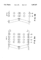
- FIG. 4 is a front view of a conventional liquid crystal display apparatus when it is driven for a long time for displaying a fixed pattern.
- FIG. 5 is a schematic sectional view of an embodiment of the liquid crystal cell according to the invention.
- FIG. 6 is a graph showing a change in cell thickness increase depending on the density of dispersed adhesive particles and polymer particles.
- thermosetting adhesive polymer particles and thermoplastic non-adhesive polymer particles are disposed in a pressed state between a pair of substrates sandwiching the liquid crystal material.
- the thermosetting adhesive particles and thermoplastic polymer particles before incorporated in the device or application of an external force thereto may suitably have an average diameter which is 1.5-5 times the cell gap, i.e., the thickness of the liquid crystal layer within the device.
- the minimum diameter of the polymer particles of 1.5 times the cell is determined because it is a minimum condition for retaining a desired columnar shape between the substrates.
- the maximum diameter of 5 times the cell gap has been determined so as to minimize an adverse effect to the alignment from experimental study.
- thermosetting adhesive particles are dispersed to suppress a shearing force to provide an improved impact-resistance between a pair of substrates.
- the dispersion density of the thermosetting adhesive particles due to occurrence of vacuum voids in the liquid crystal layer.
- the above difficulty is alleviated by dispersion of thermoplastic polymer particles in addition.
- the polymer particles comprise a thermoplastic resin, there is obtained an unexpected benefit that the deterioration of display performances can be suppressed because of an appropriate resilience of the polymer particles even when the liquid crystal device is exposed to a low temperature.
- the polymer particles are pressed and enlarged in area when they are disposed between the substrates within the liquid crystal device so that they effectively suppress the liquid crystal movement.
- thermoplastic polymer particles having a diameter of 1.5-5 times the cell when dispersed and pressed within the liquid crystal cell containing a ferroelectric liquid crystal, form columns between the substrates, which function as an obstacle to remarkably suppress the movement of liquid crystal molecules in a ferroelectric liquid crystal layer of, e.g., smectic C phase. If a polymer particles forms a column of several ⁇ m in diameter, this corresponds to several thousands of layers wherein the liquid crystal molecular movement is hindered in view of the fact that each layer spacing for liquid crystal movement is several tens of angstromes.
- the columnar structures may preferably be provided with a resilience or softness by using non-adhesive thermoplastic polymer particles in addition to the adhesive particles used for providing an increased impact resistance.
- the polymer particles may preferably comprise a thermoplastic polymer having a glass transition temperature Tg of at most -20° C.
- Tg glass transition temperature
- the polymer particles are required to be dispersed within the substrates and accordingly required to have an appropriate dispersibility.
- the low glass transition temperature characteristic is generally contradictory with the dispersibility. The contradiction can be removed by micro-encapsulating polymer particles having such a low glass transition temperature.
- FIG. 5 is a partial schematic sectional view of a liquid crystal cell according to a suitable embodiment of the present invention.
- the liquid crystal cell includes a pair of oppositely disposed glass substrates 5 respectively having on their inside surfaces ITO stripe electrodes 3 extending in mutually crossing directions, metal electrodes or wires 4 disposed on the ITO electrodes 3, insulating layers 2 and alignment films 1 further disposed inside, polymer particles 6 dispersed and pressed in adhesion between the alignment films 1, and a ferroelectric smectic liquid crystal 7 placed in a non-helical structure providing at least two stable states and filling the gap between the alignment films 1.
- the thermosetting adhesive particles are omitted from showing.
- the polymer particles 6 used in the present invention may suitably comprise a resilient material not reactive with the liquid crystal material used.
- a resilient material may include: resins, such as high-density or low-density polyethylene, acrylic urethane, nylon, acrylic resin containing a rubber, such as butyl rubber, added thereto, and silicone rubber. These materials are not exhaustive and can also be used in combination of plural species.
- the thermosetting adhesive particles may preferably be dispersed at a rate of at least 40 particles/mm 2 , more preferably at least 80 particles/mm 2 in order to provide a required impact resistance and generally at most 160 particles/mm 2 so as to avoid occurrence of vacuum voids.
- the thermoplastic non-adhesive polymer particles may preferably be dispersed at a rate of at least 40 particles, more preferably at least 80 particles/mm 2 and at most 140 particles/mm 2 so as hot to cause deterioration in image quality.
- the polymer particles may preferably be dispersed at least 80 particles/mm 2 , more preferably at least 160 particles/mm 2 and at most 300 particles/mm 2 in total.
- nylon resin particles (“SP-500M", mfd. by Toray K.K.) having an average diameter of 5 ⁇ m which was about 4 times a pre-set cell gap of 1.2 ⁇ m were suspended in IPA (isopropyl alcohol) solution and, after sufficient dispersion, the resultant dispersion was sprayed with nitrogen gas through a spray nozzle to be dispersed on an alignment film 1 of a substrate. Further, thermosetting adhesive particles of a similar diameter were dispersed at a rate of 80 particles/mm 2 as usual. Then, through an ordinary cell preparation process including application of another substrate with a sealant and curing of the sealant, a liquid crystal cell having a structure as shown in FIG. 5 was prepared. In the sealant curing step, the polymer particles were melted and pressed between the substrates to form a columnar structure as illustrated.
- SP-500M mfd. by Toray K.K.
- thermosetting adhesive particles was fixed at 80 particles/mm 2 and the dispersion rate of the polymer particles were changed in various ways.
- the cell thickness change increase ⁇ d was decreased up to a total dispersion density of 200 particles/mm 2 and at a higher dispersion density the cell thickness change was not substantially decreased any further.
- Encapsulated polymer particles were prepared by micro-encapsulating particles of acrylic methane resin having an average diameter of 5 ⁇ m which was about 4 times a set cell gap of 1.2 ⁇ m with PMMA (polymethyl methacrylate). Then, the encapsulated polymer particles were suspended and well dispersed in IPA solution and the resultant dispersion was sprayed with nitrogen gas through a spray nozzle to be dispersed at a rate of 80-140 particles/mm 2 on an alignment film 1 of a substrate. Further, thermosetting adhesive particles were dispersed at a rate of 80 particles/mm 2 as usual.
- a liquid crystal cell (panel) having a sectional structure as shown in FIG. 5 was prepared.
- the encapsulated polymer particles were pressed between the substrates to rupture the capsules and exposed the soft polymer particles therein in the step of sealant curing under pressure.
- liquid crystal panel thus prepared was stored at a low temperature of -20° C. As a result, occurrence of voids within the panel was not observed even after lapse of 240 hours.
- a liquid crystal panel prepared in a similar manner except for using polymer particles having a higher glass transition temperature caused voids therein in 12 hours.
- thermosetting adhesive particles were fixed at 80 particles/mm 2 and the dispersion rate of the polymer particles were changed in various ways.
- Example 2 the cell thickness change ⁇ d was decreased up to a total dispersion density of 200 particles/mm 2 and at a high dispersion density the cell thickness change was not substantially decreased any further.
- Three liquid crystal cells were prepared in the same manner as in Example 3 except that the polymer particles of acrylic resin containing 35% of butyl rubber, silicone rubber resin (mfd. by Toray Silicone K.K.) and low-density polyethylene resin (mfd. by Sumitomo Seika K.K.), respectively, were used.
- liquid crystal cells were subjected to a similar low-temperature storage test at -240° C. as in Example 3. In any case, no abnormality was observed even after 240 hours of the storage. In contrast thereto, a liquid crystal cell prepared in the same manner except for the use of polymer particles having a glass transition temperature exceeding -20° C. caused voids after 12-24 hours of the storage.
- thermoplastic polymer particles having a diameter 1.5-5 times the liquid crystal layer thickness between the substrates in a pressed state in addition to thermosetting adhesive particles.
- thermoplastic polymer particles having a glass transition temperature of at most -20° C. it is possible to provide an improved low-temperature storability while retaining the effect of suppressing the yellowing or occurrence of voids.
Abstract
There is provided a ferroelectric liquid crystal device wherein the yellowing due to a cell thickness increase or occurrence of voids is suppressed. The ferroelectric liquid crystal device includes a pair of substrates each having thereon a group of electrodes for liquid crystal drive, and a layer of ferroelectric liquid crystal disposed between the substrates, wherein thermosetting adhesive particles and thermoplastic polymer particles having a diameter which is 1.5-5 times the liquid crystal layer thickness are dispersed and pressed between the substrates. The polymer particles preferably have a glass transition temperature of at most -20° C.
Description
This application is a continuation of application Ser. No. 08/150,984, filed Nov. 12, 1993, now abandoned, which is a division of application Ser. No. 08/008,543, filed Jan. 25, 1993, now U.S. Pat. No. 5,285,304.
The present invention relates to a liquid crystal device using a chiral smectic liquid crystal, particularly a ferroelectric liquid crystal device wherein the increase in cell gap and occurrence of void due to movement of liquid crystal molecules during multiplexing drive are suppressed.
A display device of the type which controls transmission of light in combination with a polarizing device by utilizing the refractive index anisotropy of ferroelectric liquid crystal molecules has been proposed by Clark and Lagerwall (U.S. Pat. No. 4,367,924, etc.). The ferroelectric liquid crystal has generally chiral smectic C phase (SmC*) of H phase (SmH*) of a non-helical structure and, under this state, shows a property of taking either one of a first optically stable state and a second optically stable state responding to an electrical field applied thereto and maintaining such a state in the absence of an electrical field, namely bistability, and also has a rapid response to the change in electrical field. Thus, it is expected to be utilized in a high speed and memory type display device and particularly to provide a large-area, high-resolution display.
For an optical modulating device by use of a liquid crystal having such bistability to exhibit desirable driving characteristics, it is required that the liquid crystal disposed between a pair of substrates should be in such a molecular alignment state that conversion between the above two stable states may occur effectively irrespective of the application of an electrical field.
Further, in a liquid crystal device utilizing birefringence of a liquid crystal, the transmittance under right angle cross nicols is given by the following equation (1):
I/I.sub.O =sin.sup.2 4θsin.sup.2 (Δnd/λ)π(1)
wherein IO : incident light intensity,
I: transmitted light intensity,
θ: tilt angle,
Δn: refractive index anisotropy,
d: thickness of the liquid crystal layer,
λ: wavelength of the incident light.
The tilt angle θ in the above-mentioned non-helical structure is recognized as a half of an angle between the average molecular axis directions of liquid crystal molecules in a twisted alignment in a first orientation state and a second orientation state. According to the above equation, it is shown that a tilt angle θ of 22.5 degrees provides a maximum transmittance and the tilt angle in a non-helical structure for realizing bistability should desirably be as close as possible to 22.5 degrees.
A method for aligning a ferroelectric liquid crystal should desirably be such that molecular layers each composed of a plurality of molecules of a smectic liquid crystal are aligned uniaxially along their normals, and it is desirable to accomplish such an alignment state by a rubbing treatment which requires only a simple production step. As an alignment method for a ferroelectric liquid crystal, particularly a chiral smectic liquid crystal in a non-helical structure, one disclosed in U.S. Pat. No. 4,561,726 has been known for example.
According to our study, it has been found that, in a liquid crystal cell containing a ferroelectric liquid crystal, liquid crystal molecules per se are moved in a particular direction within the cell during drive and, as a result, the pressure is increased along a cell side to result in an increase in cell-thickness. Presumably, such a force causing the liquid crystal molecule movement may be attributable to an electrodynamic effect caused by perturbation of liquid crystal molecule dipole moments in an AC-like electric field caused by continuation of drive pulses. Further, according to our experiments, the directions 22a and 22b of the liquid crystal movement are determined in relation with the rubbing direction 20 and the average liquid crystal molecular axis position 21a or 21b as shown in FIG. 1A. As the moving direction of liquid crystal molecules is related with the rubbing direction, the above-mentioned phenomenon is assumed to depend on the pre-tilt state at the substrate surfaces. Referring to FIGS. 1A and 1B, reference numeral 21a (or 21b in a reverse orientation state) denotes an average molecular axis (director) orientation. When the liquid crystal molecules (described herein as having a negative spontaneous polarization) are oriented to provide the average molecular axis 21a and are supplied with a certain strength of AC electric field not causing a switching to the orientation state 21b, the liquid crystal molecules are liable to move in the direction of an arrow 22a in the case where the substrates are provided with rubbing axes extending in parallel and in the same direction 20. This liquid crystal movement phenomenon depends on an alignment state in the cell as described hereinbelow.
The alignment including a chevron structure of smectic layers may be explained on a model of two alignment states C1 and C2 shown in FIG. 2. Referring to FIG. 2, reference numeral 31 denotes a smectic layer showing ferroelectricity, 32 denotes a C1 alignment region, and 33 denotes a C2 alignment region. A smectic liquid crystal generally has a layer structure and causes a shrinkage of layer pitch when it is transformed from SmA (smectic A) phase into SmC (smectic C) phase or SmC* (chiral smectic C) phase, to result in a structure accompanied with a bending of layers between the upper and lower substrates 14a and 14b (chevron structure) as shown in FIG. 2. The bending of the layers 31 can be caused in two ways corresponding to the C1 and C2 alignment as shown. As is well known, liquid crystal molecules at the substrate surfaces are aligned to form a certain angle α (pre-tilt) as a result of rubbing in a direction A in such a manner that their heads (leading ends) in the rubbing direction are up (or away) from the substrate surfaces 11a and 11b. Because of the pre-tilt, the C1 and C2 alignment states are not equivalent to each other with respect to their elastic energy, and a transition between these states can be caused at a certain temperature or when supplied with a mechanical stress. When the layer structure shown in FIG. 2 is viewed in plan as shown in the upper part of FIG. 2, a boundary 34 of transition from C1 alignment (32) to C2 alignment (33) in the rubbing direction A looks like a zigzag lightning and is called a lightning defect, and a boundary 35 of transition from C2 alignment (33) to C1 alignment (32) forms a broad and moderate curve and is called a hairpin defect.
When FLC is disposed between a pair of substrates 14a and 14b and placed in an alignment state satisfying a relationship of H/ <α+δ. . . (2), wherein α denotes a pretilt angle of the FLC, H/ denotes a tilt angle (a half of cone angle), and δ denotes an angle of inclination of SmC* layer, there are four states each having a chevron structure in the C1 alignment state. These four C1 alignment states are different from the known C1 alignment state. Further, two among the four C1 alignment states form bistable states (uniform alignment). Herein, two states among the four C1 states giving an apparent tilt angle θa therebetween in the absence of an electric field satisfying a relationship of H/ >θa >H/ /2 . . . (3) are inclusively referred to as a uniform state.
In the uniform state, the directors are believed to be not twisted between the substrates in view of optical properties thereof. FIG. 3A is a schematic view illustrating director positions between the substrates in the respective states in C1 alignment. More specifically, at 51-54 are respectively shown changes in director positions between the substrates in the form of projections of directors onto cone bottoms as viewed from each bottom. At 51 and 52 is shown a splay state, and at 53 and 54 is shown a director arrangement which is believed to represent a uniform alignment state. As is understood from FIG. 3A, at 53 and 54 representing a uniform state, the molecule position (director) is different from that in the splay state either at the upper substrate or lower substrate. FIG. 3B shows two states in C2 alignment between which no switching is observed at the boundaries but an internal switching is observed. The uniform state in C1 alignment provides a larger tilt angle θa and thus a higher brightness and a higher contrast than the conventionally used bistable state in C2 alignment.
However, in a ferroelectric liquid crystal having a uniform alignment state based on the condition of H/ >θa >H/ /2, problem is liable to occur as described below in connection with the above-mentioned liquid crystal movement.
In an actual liquid crystal cell, the liquid crystal movement occurs as shown in FIG. 1A. For example, when the liquid crystal molecules in the entire cell are placed in a state providing an average molecular axis direction 21a, the liquid crystal molecules in the cell are liable to move under AC application in the direction of the arrow 22, i.e., from the right to the left in the figure. As a result, the cell thickness in a region 23 is increased gradually to show a yellowish tint. If the liquid crystal molecules are placed in a state providing an average molecular axis 21b, the liquid crystal movement under AC application is caused in the reverse direction 22b. In either case, the liquid crystal movement is caused in a direction perpendicular to the rubbing direction, i.e., in the direction of extension of smectic layers.
According to another experiment of ours, when a ferroelectric liquid crystal cell 60 including a ferroelectric liquid crystal of a non-helical structure in a high pretilt alignment state in a cell region defined by a sealant 69 is driven by a driver including a scanning electrode driver circuit 62 and a data electrode driver circuit 64 to continuously write in a white (61) or black (63) fixed pattern as shown in FIG. 4, liquid crystal molecules are caused to move in different directions B and C in parallel with the extension direction of chiral smectic C layers and perpendicular to the rubbing direction A corresponding to the molecular positions for displaying a white display state (region 61) and a black display state (region 63), respectively. As a result, at the destination sides of the liquid crystal molecular movement, the liquid crystal layer is caused to have an increased thickness while enlarging the cell gap to form portions 65 colored in pale yellow (yellowing). On the opposite sides of the liquid crystal molecular movement, voids 67 lacking liquid crystal molecules are formed. These phenomena are caused most noticeably in the neighborhood of the seal 69 and propagated toward the inside of the cell.
As described above, we have found that the liquid crystal movement in one direction is caused in a long term of drive to cause a slight change in cell thickness, thus resulting in yellowing or color deviation adversely affecting the display characteristics.
More specifically, in the destination side in the liquid crystal movement direction, the cell thickness is liable to be increased to result in a yellowish tint. On the opposite side, a state with a less amount of liquid crystal results to cause a disorder in alignment. Accordingly, a liquid crystal device causing these phenomena as a result of long term drive shows a uniformity in display performance which is much worse than the initial state, thus being accompanied with a problem in reliability.
The above-mentioned change in cell thickness causes further difficulties including changes in drive voltage threshold characteristics and adverse effects to durability of the liquid crystal device in a long term of continuous drive.
In view of the above-mentioned problems, an object of the present invention is to prevent or effectively suppress the above-mentioned yellowing or occurrence of voids due to a cell thickness increase in a ferroelectric liquid crystal device by suppressing the above-mentioned liquid crystal movement.
Another object of the present invention is to provide a ferroelectric liquid crystal device wherein the lowering or deterioration in image quality or lowering in image display quality due to the above-mentioned yellowing or occurrence of voids can be prevented or effectively suppressed.
A further object of the present invention is to provide at a low cost a ferroelectric liquid crystal device which is excellent in durability and capable of displaying high-quality images for a long period.
According to the present invention, there is provided a ferroelectric liquid crystal device, comprising: a pair of substrates each having thereon a group of electrodes for liquid crystal drive, and a layer of ferroelectric liquid crystal disposed between the substrates, wherein thermosetting adhesive particles and thermoplastic polymer particles respectively having a diameter which is 1.5-5 times the liquid crystal layer thickness are dispersed and pressed between the substrates.
According to another aspect of the present invention, there is provided a ferroelectric liquid crystal device, comprising: a pair of substrates each having thereon a group of electrodes for liquid crystal drive, and a layer of ferroelectric liquid crystal disposed between the substrates, wherein thermosetting adhesive particles and thermoplastic polymer particles having a glass transition temperature of at most -20° C. are dispersed and pressed between the substrates.
These and other objects, features and advantages of the present invention will become more apparent upon a consideration of the following description of the preferred embodiments of the present invention taken in conjunction with the accompanying drawings.
FIGS. 1A and 1B are explanatory views for illustrating a cell thickness increase along a cell side in relation with liquid crystal movement directions.
FIG. 2 is an explanatory view for illustrating an alignment state occurring in a chiral smectic liquid crystal used in the invention.
FIGS. 3A and 3B are explanatory views for illustrating changes in director orientation according to various positions between substrates in C1 alignment and C2 alignment, respectively.
FIG. 4 is a front view of a conventional liquid crystal display apparatus when it is driven for a long time for displaying a fixed pattern.
FIG. 5 is a schematic sectional view of an embodiment of the liquid crystal cell according to the invention.
FIG. 6 is a graph showing a change in cell thickness increase depending on the density of dispersed adhesive particles and polymer particles.
In the liquid crystal device according to the present invention, thermosetting adhesive polymer particles and thermoplastic non-adhesive polymer particles are disposed in a pressed state between a pair of substrates sandwiching the liquid crystal material. The thermosetting adhesive particles and thermoplastic polymer particles before incorporated in the device or application of an external force thereto may suitably have an average diameter which is 1.5-5 times the cell gap, i.e., the thickness of the liquid crystal layer within the device.
The minimum diameter of the polymer particles of 1.5 times the cell is determined because it is a minimum condition for retaining a desired columnar shape between the substrates. On the other hand, the maximum diameter of 5 times the cell gap has been determined so as to minimize an adverse effect to the alignment from experimental study.
As in a conventional device thermosetting adhesive particles are dispersed to suppress a shearing force to provide an improved impact-resistance between a pair of substrates. However, there is a certain limit for the dispersion density of the thermosetting adhesive particles due to occurrence of vacuum voids in the liquid crystal layer. In the present invention, the above difficulty is alleviated by dispersion of thermoplastic polymer particles in addition. As the polymer particles comprise a thermoplastic resin, there is obtained an unexpected benefit that the deterioration of display performances can be suppressed because of an appropriate resilience of the polymer particles even when the liquid crystal device is exposed to a low temperature.
The polymer particles are pressed and enlarged in area when they are disposed between the substrates within the liquid crystal device so that they effectively suppress the liquid crystal movement.
More specifically, the thermoplastic polymer particles having a diameter of 1.5-5 times the cell, when dispersed and pressed within the liquid crystal cell containing a ferroelectric liquid crystal, form columns between the substrates, which function as an obstacle to remarkably suppress the movement of liquid crystal molecules in a ferroelectric liquid crystal layer of, e.g., smectic C phase. If a polymer particles forms a column of several μm in diameter, this corresponds to several thousands of layers wherein the liquid crystal molecular movement is hindered in view of the fact that each layer spacing for liquid crystal movement is several tens of angstromes. When a movement of a liquid crystal molecule within a layer is suppressed, the molecule cannot but change moving torque into a direction crossing the layers, but the movement across the layers requires a larger torque by almost one digit. As a result, because of the presence of the obstacle (column), the velocity of the liquid crystals moving along a layer which is traversed by the column is lowered by nearly one digit. Accordingly, the movement of liquid crystal molecules along the liquid crystal molecular layer is suppressed.
When the adaptability of a ferroelectric liquid crystal panel to storage at a lower temperature is considered, in case where rigid columnar structures are present within the panel, the columnar structures under a volumetric shrinkage between the substrates upon cooling and on the other hand the liquid crystal contained therein causes a shrinkage regardless of the columnar structures. As a result, there can be formed voids within the cell in some cases because the cell shrinkage fails to follow the liquid crystal shrinkage.
In order to cope with the problem, in the present invention, the columnar structures may preferably be provided with a resilience or softness by using non-adhesive thermoplastic polymer particles in addition to the adhesive particles used for providing an increased impact resistance. In order to provide a better low-temperature storability, the polymer particles may preferably comprise a thermoplastic polymer having a glass transition temperature Tg of at most -20° C. On the other hand, the polymer particles are required to be dispersed within the substrates and accordingly required to have an appropriate dispersibility. The low glass transition temperature characteristic is generally contradictory with the dispersibility. The contradiction can be removed by micro-encapsulating polymer particles having such a low glass transition temperature.
Hereinbelow, some embodiments of the present invention will be described with reference to drawings.
FIG. 5 is a partial schematic sectional view of a liquid crystal cell according to a suitable embodiment of the present invention. Referring to FIG. 5, the liquid crystal cell includes a pair of oppositely disposed glass substrates 5 respectively having on their inside surfaces ITO stripe electrodes 3 extending in mutually crossing directions, metal electrodes or wires 4 disposed on the ITO electrodes 3, insulating layers 2 and alignment films 1 further disposed inside, polymer particles 6 dispersed and pressed in adhesion between the alignment films 1, and a ferroelectric smectic liquid crystal 7 placed in a non-helical structure providing at least two stable states and filling the gap between the alignment films 1. In FIG. 5, the thermosetting adhesive particles are omitted from showing.
The polymer particles 6 used in the present invention may suitably comprise a resilient material not reactive with the liquid crystal material used. Examples of such material may include: resins, such as high-density or low-density polyethylene, acrylic urethane, nylon, acrylic resin containing a rubber, such as butyl rubber, added thereto, and silicone rubber. These materials are not exhaustive and can also be used in combination of plural species.
The thermosetting adhesive particles may preferably be dispersed at a rate of at least 40 particles/mm2, more preferably at least 80 particles/mm2 in order to provide a required impact resistance and generally at most 160 particles/mm2 so as to avoid occurrence of vacuum voids. On the other hand, the thermoplastic non-adhesive polymer particles may preferably be dispersed at a rate of at least 40 particles, more preferably at least 80 particles/mm2 and at most 140 particles/mm2 so as hot to cause deterioration in image quality. Accordingly, the polymer particles may preferably be dispersed at least 80 particles/mm2, more preferably at least 160 particles/mm2 and at most 300 particles/mm2 in total.
In order to form a columnar structure of polymer particles 6, nylon resin particles ("SP-500M", mfd. by Toray K.K.) having an average diameter of 5 μm which was about 4 times a pre-set cell gap of 1.2 μm were suspended in IPA (isopropyl alcohol) solution and, after sufficient dispersion, the resultant dispersion was sprayed with nitrogen gas through a spray nozzle to be dispersed on an alignment film 1 of a substrate. Further, thermosetting adhesive particles of a similar diameter were dispersed at a rate of 80 particles/mm2 as usual. Then, through an ordinary cell preparation process including application of another substrate with a sealant and curing of the sealant, a liquid crystal cell having a structure as shown in FIG. 5 was prepared. In the sealant curing step, the polymer particles were melted and pressed between the substrates to form a columnar structure as illustrated.
Several cells were prepared in the same manner as in Example 1 except that the dispersion rate of the thermosetting adhesive particles was fixed at 80 particles/mm2 and the dispersion rate of the polymer particles were changed in various ways.
The resultant cells were subjected to 100 hours of drive test under application of rectangular pulses of Vop=20 volts at 30° C., and the resultant maximum cell increase for each cell was measured. The results are shown in FIG. 6.
As is shown in FIG. 6, the cell thickness change increase Δd was decreased up to a total dispersion density of 200 particles/mm2 and at a higher dispersion density the cell thickness change was not substantially decreased any further.
Encapsulated polymer particles were prepared by micro-encapsulating particles of acrylic methane resin having an average diameter of 5 μm which was about 4 times a set cell gap of 1.2 μm with PMMA (polymethyl methacrylate). Then, the encapsulated polymer particles were suspended and well dispersed in IPA solution and the resultant dispersion was sprayed with nitrogen gas through a spray nozzle to be dispersed at a rate of 80-140 particles/mm2 on an alignment film 1 of a substrate. Further, thermosetting adhesive particles were dispersed at a rate of 80 particles/mm2 as usual.
Then, through an ordinary cell application process, a liquid crystal cell (panel) having a sectional structure as shown in FIG. 5 was prepared. During the cell preparation, the encapsulated polymer particles were pressed between the substrates to rupture the capsules and exposed the soft polymer particles therein in the step of sealant curing under pressure.
Then, the liquid crystal panel thus prepared was stored at a low temperature of -20° C. As a result, occurrence of voids within the panel was not observed even after lapse of 240 hours. In contrast thereto, a liquid crystal panel prepared in a similar manner except for using polymer particles having a higher glass transition temperature (i.e., in the same manner as in Example 1) caused voids therein in 12 hours.
The above results show that the use of encapsulated polymer particles having a low glass transition point for dispersion within a cell could prevent occurrence of voids during low-temperature storage while preventing the occurrence of yellowing or voids during operation.
Several cells were prepared in the same manner as in Example 3 except that the dispersion rate of the thermosetting adhesive particles were fixed at 80 particles/mm2 and the dispersion rate of the polymer particles were changed in various ways.
The resultant cells were subjected to 100 hours of drive test under application of rectangular pulses of Vop=20 volts at 30° C., and the resultant maximum cell thickness increase for each cell was measured in the same manner as in Example 2.
Similarly as in Example 2, the cell thickness change Δd was decreased up to a total dispersion density of 200 particles/mm2 and at a high dispersion density the cell thickness change was not substantially decreased any further.
Three liquid crystal cells were prepared in the same manner as in Example 3 except that the polymer particles of acrylic resin containing 35% of butyl rubber, silicone rubber resin (mfd. by Toray Silicone K.K.) and low-density polyethylene resin (mfd. by Sumitomo Seika K.K.), respectively, were used.
Then, the liquid crystal cells were subjected to a similar low-temperature storage test at -240° C. as in Example 3. In any case, no abnormality was observed even after 240 hours of the storage. In contrast thereto, a liquid crystal cell prepared in the same manner except for the use of polymer particles having a glass transition temperature exceeding -20° C. caused voids after 12-24 hours of the storage.
As described above, according to the present invention, it is possible to remarkably suppress the occurrence of yellowing or voids due to movement of liquid crystal molecules even after a long time of drive by dispersing thermoplastic polymer particles having a diameter 1.5-5 times the liquid crystal layer thickness between the substrates in a pressed state in addition to thermosetting adhesive particles.
Further, by using thermoplastic polymer particles having a glass transition temperature of at most -20° C., it is possible to provide an improved low-temperature storability while retaining the effect of suppressing the yellowing or occurrence of voids.
Further, by using such polymer particles in an encapsulated form, it is possible to improve the dispersibility of the polymer particles whereby it is possible to enhance the effect of suppressing liquid crystal movement and further improve the display quality.
Claims (8)
1. A ferroelectric liquid crystal device, comprising: a pair of substrates each having thereon a group of electrodes for driving a liquid crystal, and a ferroelectric liquid crystal layer disposed between the substrates, said ferroelectric liquid crystal being in a uniform alignment state satisfying a relationship of H/ >θa>/2, wherein H/ denotes a half of cone angle and θa denotes an apparent tilt angle of the ferroelectric liquid crystal, said liquid crystal device further comprising thermosetting adhesive particles and resilient thermoplastic polymer particles dispersed between the substrates in densities sufficient to suppress movement of the ferroelectric liquid crystal along the surfaces of the substrates, said thermoplastic polymer particles having a columnar shape; wherein
molecules of the ferroelectric liquid crystal are aligned inclined to the surfaces of both substrates, and
the ferroelectric liquid crystal comprises a plurality of molecular layers each composed of plural molecules in which both the liquid crystal molecules and the molecular layers are aligned inclined to the surfaces of both substrates.
2. A device according to claim 1, wherein said polymer particles are dispersed at a density of at least 40 particles/mm2 and said adhesive particles are dispersed at a density of at least 40 particles/mm2.
3. A device according to claim 1, wherein said polymer particles comprise at least one material selected from the group consisting of high-density polyethylene, low-density polyethylene, acrylic urethane resin, acrylic resin containing butyl rubber, nylon and silicon rubber resin.
4. A liquid crystal device, comprising:
a pair of substrates, and a chiral smectic liquid crystal disposed between the substrates, wherein
molecules of the chiral smectic liquid crystal are aligned inclined to the surfaces of both substrates,
the chiral smectic liquid crystal molecules form a plurality of smectic layers aligned inclined to the surfaces of both substrates, and having
thermosetting adhesive particles and resilient thermoplastic polymer particles dispersed between the substrates in densities sufficient to suppress movement of the liquid crystal along the surfaces of the substrates, said thermoplastic polymer particles having a columnar shape.
5. A device according to claim 4, wherein said plurality of smectic layers are uniformly bent in one direction.
6. A device according to claim 4, wherein said polymer particles are dispersed at a density of at least 40 particles/mm2 and said adhesive particles are dispersed at a density of at least 40 particles/mm2.
7. A liquid crystal device comprising:
a pair of substrates, a chiral smectic liquid crystal disposed between the substrates, and thermoplastic polymer particles dispersed between the substrates, wherein said thermoplastic polymer particles are resilient and dispersed at a density of at least 80 particles/mm2 and disposed in a columnar shape.
8. A device according to claim 7, wherein said thermoplastic polymer particles have a glass transition point of at most -20° C.
Priority Applications (1)
| Application Number | Priority Date | Filing Date | Title |
|---|---|---|---|
| US08/483,156 US5497257A (en) | 1992-01-24 | 1995-06-07 | Ferroelectric liquid crystal device |
Applications Claiming Priority (7)
| Application Number | Priority Date | Filing Date | Title |
|---|---|---|---|
| JP3286592 | 1992-01-24 | ||
| JP4-032865 | 1992-01-24 | ||
| JP4-034029 | 1992-01-27 | ||
| JP3402992 | 1992-01-27 | ||
| US08/008,543 US5285304A (en) | 1992-01-24 | 1993-01-25 | Ferroelectric liquid crystal device having spacers including the thermosetting adhesive particles and the thermoplastic polymer particles |
| US15098493A | 1993-11-12 | 1993-11-12 | |
| US08/483,156 US5497257A (en) | 1992-01-24 | 1995-06-07 | Ferroelectric liquid crystal device |
Related Parent Applications (1)
| Application Number | Title | Priority Date | Filing Date |
|---|---|---|---|
| US15098493A Continuation | 1992-01-24 | 1993-11-12 |
Publications (1)
| Publication Number | Publication Date |
|---|---|
| US5497257A true US5497257A (en) | 1996-03-05 |
Family
ID=26371456
Family Applications (3)
| Application Number | Title | Priority Date | Filing Date |
|---|---|---|---|
| US08/008,543 Expired - Fee Related US5285304A (en) | 1992-01-24 | 1993-01-25 | Ferroelectric liquid crystal device having spacers including the thermosetting adhesive particles and the thermoplastic polymer particles |
| US08/476,768 Expired - Fee Related US5581384A (en) | 1992-01-24 | 1995-06-07 | Process for producing a display device by deforming thermoplastic spacer particles |
| US08/483,156 Expired - Fee Related US5497257A (en) | 1992-01-24 | 1995-06-07 | Ferroelectric liquid crystal device |
Family Applications Before (2)
| Application Number | Title | Priority Date | Filing Date |
|---|---|---|---|
| US08/008,543 Expired - Fee Related US5285304A (en) | 1992-01-24 | 1993-01-25 | Ferroelectric liquid crystal device having spacers including the thermosetting adhesive particles and the thermoplastic polymer particles |
| US08/476,768 Expired - Fee Related US5581384A (en) | 1992-01-24 | 1995-06-07 | Process for producing a display device by deforming thermoplastic spacer particles |
Country Status (1)
| Country | Link |
|---|---|
| US (3) | US5285304A (en) |
Cited By (5)
| Publication number | Priority date | Publication date | Assignee | Title |
|---|---|---|---|---|
| US5851605A (en) * | 1995-12-26 | 1998-12-22 | Matsushita Electric Industrial Co., Ltd. | Adhesive particulate composition, adhesive spacers for liquid crystal display panel, and liquid crystal display panel |
| US5858273A (en) * | 1995-07-27 | 1999-01-12 | Canon Kabushiki Kaisha | Liquid crystal device |
| US5860212A (en) * | 1994-03-30 | 1999-01-19 | Seiko Instruments Inc. | Method of coating a conductive substance on a transparent electrode formed on a substrate and method of mounting a semiconductor device or film substrate on the substrate |
| US5885482A (en) * | 1995-12-28 | 1999-03-23 | Canon Kabushiki Kaisha | Liquid crystal device, production process thereof and liquid crystal apparatus |
| US6122032A (en) * | 1996-07-31 | 2000-09-19 | Canon Kabushiki Kaisha | Wedge shaped LCD with change in dispersion density of spacers |
Families Citing this family (17)
| Publication number | Priority date | Publication date | Assignee | Title |
|---|---|---|---|---|
| US5467209A (en) * | 1992-01-24 | 1995-11-14 | Canon Kabushiki Kaisha | Ferroelectric liquid crystal device with particular layer thicknesses at non-pixel portions and pixel portions |
| US5285304A (en) * | 1992-01-24 | 1994-02-08 | Canon Kabushiki Kaisha | Ferroelectric liquid crystal device having spacers including the thermosetting adhesive particles and the thermoplastic polymer particles |
| SE503136C2 (en) | 1994-12-09 | 1996-04-01 | Emt Ag | Pressure resistant liquid crystal cell |
| US5921285A (en) * | 1995-09-28 | 1999-07-13 | Fiberspar Spoolable Products, Inc. | Composite spoolable tube |
| KR970048809A (en) * | 1995-12-30 | 1997-07-29 | 손욱 | LCD with Elastic Adhesive Spacers |
| CH691710A5 (en) * | 1997-07-07 | 2001-09-14 | Asulab Sa | A method of manufacturing a batch of cells and lamellar lamellar cells thus obtained. |
| JP4028043B2 (en) * | 1997-10-03 | 2007-12-26 | コニカミノルタホールディングス株式会社 | Liquid crystal light modulation device and method for manufacturing liquid crystal light modulation device |
| JP3760645B2 (en) | 1998-11-11 | 2006-03-29 | コニカミノルタホールディングス株式会社 | Manufacturing method of liquid crystal light modulation device |
| JP2001042339A (en) | 1999-08-02 | 2001-02-16 | Minolta Co Ltd | Liquid crystal optical modulation device |
| US6697143B2 (en) | 2001-02-12 | 2004-02-24 | Viztec, Inc. | Electrooptical displays constructed with polymerization initiating and enhancing elements positioned between substrates |
| US6606142B2 (en) * | 2001-02-12 | 2003-08-12 | Viztec, Inc. | Electrooptical displays with polymer localized in vicinities of substrate spacers |
| US6618114B2 (en) | 2001-02-12 | 2003-09-09 | Viztec, Inc. | Electrooptical displays with multilayer structure achieved by varying rates of polymerization and/or phase separation during the course of polymerization |
| JP3977997B2 (en) * | 2001-05-11 | 2007-09-19 | 松下電器産業株式会社 | Semiconductor device and manufacturing method thereof |
| US6621548B2 (en) * | 2001-06-15 | 2003-09-16 | Viztec, Inc. | Electrooptical displays constructed with polymer-coated elements positioned between substrates |
| US7179512B2 (en) * | 2002-05-14 | 2007-02-20 | Fujitsu Limited | Liquid crystal display and manufacturing method of same |
| CN103323982B (en) | 2013-06-20 | 2015-09-23 | 北京京东方光电科技有限公司 | A kind of display panels and manufacture method thereof |
| JP6900279B2 (en) | 2016-09-13 | 2021-07-07 | キヤノン株式会社 | Toner and toner manufacturing method |
Citations (21)
| Publication number | Priority date | Publication date | Assignee | Title |
|---|---|---|---|---|
| US4367924A (en) * | 1980-01-08 | 1983-01-11 | Clark Noel A | Chiral smectic C or H liquid crystal electro-optical device |
| JPS5984220A (en) * | 1982-11-05 | 1984-05-15 | Seiko Epson Corp | Liquid crystal display body |
| US4561726A (en) * | 1983-07-29 | 1985-12-31 | At&T Bell Laboratories | Alignment of ferroelectric LCDs |
| US4712877A (en) * | 1985-01-18 | 1987-12-15 | Canon Kabushiki Kaisha | Ferroelectric display panel of varying thickness and driving method therefor |
| US4712875A (en) * | 1985-05-15 | 1987-12-15 | Canon Kabushiki Kaisha | Dimensions of spacer particles for a ferroelectric liquid crystal display |
| US4728176A (en) * | 1985-10-17 | 1988-03-01 | Canon Kabushiki Kaisha | Ferroelectric liquid crystal device with metallic auxiliary electrodes provided adjacent to the transparent electrodes |
| US4740060A (en) * | 1985-12-24 | 1988-04-26 | Canon Kabushiki Kaisha | Electro-optical device having heat-bondable and non-heat-bondable gap controllers |
| US4775225A (en) * | 1985-05-16 | 1988-10-04 | Canon Kabushiki Kaisha | Liquid crystal device having pillar spacers with small base periphery width in direction perpendicular to orientation treatment |
| JPH0296119A (en) * | 1988-09-30 | 1990-04-06 | Toray Ind Inc | Liquid crystal display device made of film substrate and production thereof |
| US4932758A (en) * | 1987-09-17 | 1990-06-12 | Canon Kabushiki Kaisha | Ferroelectric smectic liquid crystal device having a bistable alignment state providing two stable orientation states |
| US4989955A (en) * | 1985-09-25 | 1991-02-05 | Toray Industries, Inc. | Liquid crystal electro-optical element and process for preparation thereof |
| US5007716A (en) * | 1988-01-11 | 1991-04-16 | Canon Kabushiki Kaisha | Liquid crystal device |
| US5013137A (en) * | 1985-09-04 | 1991-05-07 | Canon Kabushiki Kaisha | Ferroelectric liquid crystal device having increased tilt angle |
| JPH03160416A (en) * | 1989-11-20 | 1991-07-10 | Toshiba Corp | Production of liquid crystal display device |
| US5054890A (en) * | 1988-06-23 | 1991-10-08 | Canon Kabushiki Kaisha | Liquid crystal device |
| US5099344A (en) * | 1987-06-12 | 1992-03-24 | Canon Kabushiki Kaisha | Ferroelectric liquid crystal device |
| US5103331A (en) * | 1988-08-04 | 1992-04-07 | Canon Kabushiki Kaisha | Liquid crystal cell having substantially uniform distribution of spacers and non-uniform distribution of particulate adhesive |
| US5109294A (en) * | 1989-03-07 | 1992-04-28 | Canon Kabushiki Kaisha | Liquid crystal apparatus having a liquid crystal panel and a panel supporting means |
| US5165076A (en) * | 1987-06-12 | 1992-11-17 | Canon Kabushiki Kaisha | Ferroelectric liquid crystal device with particular primer alignment, and liquid crystal layers |
| US5189536A (en) * | 1990-03-02 | 1993-02-23 | Canon Kabushiki Kaisha | Ferroelectric liquid crystal element having uniform high temperature alignment |
| US5285304A (en) * | 1992-01-24 | 1994-02-08 | Canon Kabushiki Kaisha | Ferroelectric liquid crystal device having spacers including the thermosetting adhesive particles and the thermoplastic polymer particles |
Family Cites Families (8)
| Publication number | Priority date | Publication date | Assignee | Title |
|---|---|---|---|---|
| JPS5729031A (en) * | 1980-07-28 | 1982-02-16 | Nissan Motor Co Ltd | Liquid crystal display panel |
| DE3400429A1 (en) * | 1984-01-09 | 1985-07-18 | Vdo Adolf Schindling Ag, 6000 Frankfurt | DISPLAY DEVICE, ESPECIALLY LIQUID CRYSTAL DISPLAY, AND METHOD FOR THE PRODUCTION THEREOF |
| JPS628128A (en) * | 1985-07-05 | 1987-01-16 | Seiko Epson Corp | Liquid crystal display device |
| JPS6273232A (en) * | 1985-09-27 | 1987-04-03 | Sharp Corp | Liquid crystal display panel |
| JPH0196626A (en) * | 1987-10-07 | 1989-04-14 | Sharp Corp | Liquid crystal display panel |
| US4973138A (en) * | 1987-10-27 | 1990-11-27 | Semiconductor Energy Laboratory Co., Ltd. | Liquid crystal device and manufacturing method for the same |
| JPH01113729A (en) * | 1987-10-27 | 1989-05-02 | Semiconductor Energy Lab Co Ltd | Liquid crystal electro-optic device |
| JP2814089B2 (en) * | 1988-12-12 | 1998-10-22 | 株式会社半導体エネルギー研究所 | Liquid crystal electro-optical device |
-
1993
- 1993-01-25 US US08/008,543 patent/US5285304A/en not_active Expired - Fee Related
-
1995
- 1995-06-07 US US08/476,768 patent/US5581384A/en not_active Expired - Fee Related
- 1995-06-07 US US08/483,156 patent/US5497257A/en not_active Expired - Fee Related
Patent Citations (21)
| Publication number | Priority date | Publication date | Assignee | Title |
|---|---|---|---|---|
| US4367924A (en) * | 1980-01-08 | 1983-01-11 | Clark Noel A | Chiral smectic C or H liquid crystal electro-optical device |
| JPS5984220A (en) * | 1982-11-05 | 1984-05-15 | Seiko Epson Corp | Liquid crystal display body |
| US4561726A (en) * | 1983-07-29 | 1985-12-31 | At&T Bell Laboratories | Alignment of ferroelectric LCDs |
| US4712877A (en) * | 1985-01-18 | 1987-12-15 | Canon Kabushiki Kaisha | Ferroelectric display panel of varying thickness and driving method therefor |
| US4712875A (en) * | 1985-05-15 | 1987-12-15 | Canon Kabushiki Kaisha | Dimensions of spacer particles for a ferroelectric liquid crystal display |
| US4775225A (en) * | 1985-05-16 | 1988-10-04 | Canon Kabushiki Kaisha | Liquid crystal device having pillar spacers with small base periphery width in direction perpendicular to orientation treatment |
| US5013137A (en) * | 1985-09-04 | 1991-05-07 | Canon Kabushiki Kaisha | Ferroelectric liquid crystal device having increased tilt angle |
| US4989955A (en) * | 1985-09-25 | 1991-02-05 | Toray Industries, Inc. | Liquid crystal electro-optical element and process for preparation thereof |
| US4728176A (en) * | 1985-10-17 | 1988-03-01 | Canon Kabushiki Kaisha | Ferroelectric liquid crystal device with metallic auxiliary electrodes provided adjacent to the transparent electrodes |
| US4740060A (en) * | 1985-12-24 | 1988-04-26 | Canon Kabushiki Kaisha | Electro-optical device having heat-bondable and non-heat-bondable gap controllers |
| US5099344A (en) * | 1987-06-12 | 1992-03-24 | Canon Kabushiki Kaisha | Ferroelectric liquid crystal device |
| US5165076A (en) * | 1987-06-12 | 1992-11-17 | Canon Kabushiki Kaisha | Ferroelectric liquid crystal device with particular primer alignment, and liquid crystal layers |
| US4932758A (en) * | 1987-09-17 | 1990-06-12 | Canon Kabushiki Kaisha | Ferroelectric smectic liquid crystal device having a bistable alignment state providing two stable orientation states |
| US5007716A (en) * | 1988-01-11 | 1991-04-16 | Canon Kabushiki Kaisha | Liquid crystal device |
| US5054890A (en) * | 1988-06-23 | 1991-10-08 | Canon Kabushiki Kaisha | Liquid crystal device |
| US5103331A (en) * | 1988-08-04 | 1992-04-07 | Canon Kabushiki Kaisha | Liquid crystal cell having substantially uniform distribution of spacers and non-uniform distribution of particulate adhesive |
| JPH0296119A (en) * | 1988-09-30 | 1990-04-06 | Toray Ind Inc | Liquid crystal display device made of film substrate and production thereof |
| US5109294A (en) * | 1989-03-07 | 1992-04-28 | Canon Kabushiki Kaisha | Liquid crystal apparatus having a liquid crystal panel and a panel supporting means |
| JPH03160416A (en) * | 1989-11-20 | 1991-07-10 | Toshiba Corp | Production of liquid crystal display device |
| US5189536A (en) * | 1990-03-02 | 1993-02-23 | Canon Kabushiki Kaisha | Ferroelectric liquid crystal element having uniform high temperature alignment |
| US5285304A (en) * | 1992-01-24 | 1994-02-08 | Canon Kabushiki Kaisha | Ferroelectric liquid crystal device having spacers including the thermosetting adhesive particles and the thermoplastic polymer particles |
Cited By (5)
| Publication number | Priority date | Publication date | Assignee | Title |
|---|---|---|---|---|
| US5860212A (en) * | 1994-03-30 | 1999-01-19 | Seiko Instruments Inc. | Method of coating a conductive substance on a transparent electrode formed on a substrate and method of mounting a semiconductor device or film substrate on the substrate |
| US5858273A (en) * | 1995-07-27 | 1999-01-12 | Canon Kabushiki Kaisha | Liquid crystal device |
| US5851605A (en) * | 1995-12-26 | 1998-12-22 | Matsushita Electric Industrial Co., Ltd. | Adhesive particulate composition, adhesive spacers for liquid crystal display panel, and liquid crystal display panel |
| US5885482A (en) * | 1995-12-28 | 1999-03-23 | Canon Kabushiki Kaisha | Liquid crystal device, production process thereof and liquid crystal apparatus |
| US6122032A (en) * | 1996-07-31 | 2000-09-19 | Canon Kabushiki Kaisha | Wedge shaped LCD with change in dispersion density of spacers |
Also Published As
| Publication number | Publication date |
|---|---|
| US5285304A (en) | 1994-02-08 |
| US5581384A (en) | 1996-12-03 |
Similar Documents
| Publication | Publication Date | Title |
|---|---|---|
| US5497257A (en) | Ferroelectric liquid crystal device | |
| EP0550846B1 (en) | Ferroelectric liquid crystal device and process for production thereof | |
| KR100320320B1 (en) | Liquid crystal display device | |
| US4682858A (en) | Liquid crystal device having reduced-pressure region in communication with ferroelectric liquid crystal | |
| EP1992985B1 (en) | Method of driving a liquid crystal display | |
| US4744639A (en) | Ferroelectric liquid crystal device having a flattening layer | |
| JP3217884B2 (en) | Liquid crystal display device and device | |
| US5956112A (en) | Liquid crystal display device and method for manufacturing the same | |
| JPS60220316A (en) | Liquid crystal optical element | |
| US5822031A (en) | Liquid crystal device | |
| US6320639B1 (en) | Liquid crystal device and process for production thereof | |
| US7477349B2 (en) | Bistable nematic liquid crystal device | |
| US5204766A (en) | Ferroelectric liquid crystal cell with particulate adhesive density higher near side | |
| US5452114A (en) | Ferroelectric liquid crystal device with grooves between electrode on one substrate, ridges on the other | |
| US5589964A (en) | Ferroelectric liquid crystal device with minute convexities between adjacent electrodes | |
| US5748274A (en) | LCD having a voltage being applied to the LC in the chiral nematic phase prior to the display driving | |
| EP0750213B1 (en) | Method of producing a ferroelectric liquid crystal display device | |
| US6154267A (en) | Method of fabricating a liquid crystal display device including a liquid crystal region surrounded by a polymer material | |
| US6847418B2 (en) | Liquid crystal display panel implementing bistable liquid crystal and method of fabricating the same | |
| JPH05273561A (en) | Ferroelectric liquid crystal element | |
| US5726725A (en) | Liquid crystal device and process for production thereof with polyimide alignment film rubbed and then baked | |
| JPH07199174A (en) | Liquid crystal display element | |
| JP3205250B2 (en) | Liquid crystal element and manufacturing method thereof | |
| JPS61205921A (en) | Liquid crystal element | |
| JPH05313126A (en) | Liquid crystal display element |
Legal Events
| Date | Code | Title | Description |
|---|---|---|---|
| CC | Certificate of correction | ||
| FPAY | Fee payment |
Year of fee payment: 4 |
|
| FEPP | Fee payment procedure |
Free format text: PAYOR NUMBER ASSIGNED (ORIGINAL EVENT CODE: ASPN); ENTITY STATUS OF PATENT OWNER: LARGE ENTITY Free format text: PAYER NUMBER DE-ASSIGNED (ORIGINAL EVENT CODE: RMPN); ENTITY STATUS OF PATENT OWNER: LARGE ENTITY |
|
| FPAY | Fee payment |
Year of fee payment: 8 |
|
| REMI | Maintenance fee reminder mailed | ||
| LAPS | Lapse for failure to pay maintenance fees | ||
| STCH | Information on status: patent discontinuation |
Free format text: PATENT EXPIRED DUE TO NONPAYMENT OF MAINTENANCE FEES UNDER 37 CFR 1.362 |
|
| FP | Lapsed due to failure to pay maintenance fee |
Effective date: 20080305 |