US5486842A - On-screen display circuit of the interlaced scanning type - Google Patents
On-screen display circuit of the interlaced scanning type Download PDFInfo
- Publication number
- US5486842A US5486842A US08/368,960 US36896095A US5486842A US 5486842 A US5486842 A US 5486842A US 36896095 A US36896095 A US 36896095A US 5486842 A US5486842 A US 5486842A
- Authority
- US
- United States
- Prior art keywords
- vertical
- address
- decoded
- decoder
- bit
- Prior art date
- Legal status (The legal status is an assumption and is not a legal conclusion. Google has not performed a legal analysis and makes no representation as to the accuracy of the status listed.)
- Expired - Lifetime
Links
Images


Classifications
-
- H—ELECTRICITY
- H04—ELECTRIC COMMUNICATION TECHNIQUE
- H04N—PICTORIAL COMMUNICATION, e.g. TELEVISION
- H04N5/00—Details of television systems
- H04N5/44—Receiver circuitry for the reception of television signals according to analogue transmission standards
- H04N5/445—Receiver circuitry for the reception of television signals according to analogue transmission standards for displaying additional information
-
- G—PHYSICS
- G09—EDUCATION; CRYPTOGRAPHY; DISPLAY; ADVERTISING; SEALS
- G09G—ARRANGEMENTS OR CIRCUITS FOR CONTROL OF INDICATING DEVICES USING STATIC MEANS TO PRESENT VARIABLE INFORMATION
- G09G5/00—Control arrangements or circuits for visual indicators common to cathode-ray tube indicators and other visual indicators
- G09G5/22—Control arrangements or circuits for visual indicators common to cathode-ray tube indicators and other visual indicators characterised by the display of characters or indicia using display control signals derived from coded signals representing the characters or indicia, e.g. with a character-code memory
- G09G5/222—Control of the character-code memory
-
- H—ELECTRICITY
- H04—ELECTRIC COMMUNICATION TECHNIQUE
- H04N—PICTORIAL COMMUNICATION, e.g. TELEVISION
- H04N5/00—Details of television systems
- H04N5/44—Receiver circuitry for the reception of television signals according to analogue transmission standards
- H04N5/445—Receiver circuitry for the reception of television signals according to analogue transmission standards for displaying additional information
- H04N5/44504—Circuit details of the additional information generator, e.g. details of the character or graphics signal generator, overlay mixing circuits
Definitions
- the present invention relates in general to on-screen display circuits, and more particularly to an on-screen display circuit of the interlaced scanning type for displaying a character or picture on a screen in an interlaced scanning manner to double a definition degree.
- an on-screen display (referred to hereinafter as OSD) function is to display a desired character or picture on a desired position of a screen.
- OSD on-screen display
- FIG. 1 there is shown a block diagram of a conventional OSD circuit performing the OSD function.
- the conventional OSD circuit comprises a vertical counter 1 for counting a horizontal synchronous signal H-SYNC inputted thereto, a vertical decoder 2 for decoding an output signal from the vertical counter 1 and outputting the decoded signal to designate a decoded vertical address, a character decoder 3 for decoding a character address inputted thereto and outputting the decoded signal to designate a decoded horizontal address, and a font read only memory (referred to hereinafter as ROM) 4 for storing information regarding characters or pictures to be displayed on the screen and outputting font data in its location corresponding to the decoded vertical address from the vertical decoder 2 and the decoded horizontal address from the character decoder 3.
- ROM font read only memory
- the horizontal synchronous signal H-SYNC is separated from a broadcasting signal and then applied to the vertical counter 1.
- the vertical counter 1 Upon inputting the horizontal synchronous signal H-SYNC, the vertical counter 1 counts the inputted horizontal synchronous signal H-SYNC and, as a result of the counting operation, outputs the vertical address to the vertical decoder 2, the vertical address designating a vertical dot of a font to be displayed on the screen.
- the vertical decoder 2 decodes the vertical address from the vertical counter 1 and outputs the decoded signal to the font ROM 4 to designate the decoded vertical address thereof.
- the character decoder 3 decodes the inputted character address and outputs the decoded signal to the font ROM 4 to designate the decoded horizontal address thereof.
- the font ROM 4 outputs the font data in its location corresponding to the decoded vertical address from the vertical decoder 2 and the decoded horizontal address from the character decoder 3.
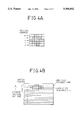
- the decoded vertical decoder 2 is adapted to designate the vertical address of the font to be displayed on the screen using merely the counted value of the horizontal synchronous signal H-SYNC with no consideration for an interlaced scanning manner. For this reason, in the case where the addresses of the font are designated as shown in FIG. 2A, the same character or picture is displayed in both odd and even fields of a video signal as shown in FIG. 2B.
- the above-mentioned conventional OSD circuit has a disadvantage in that the same dot data is displayed in both the odd and even fields of the video signal, resulting in a reduction in a resolution by half.
- the present invention has been made in view of the above problem, and it is an object of the present invention to provide an OSD circuit of the interlaced scanning type for outputting dot data of a character or picture to be displayed on a screen in an interlaced scanning manner to enhance a resolution of the displayed character or picture.
- an on-screen display circuit of the interlaced scanning type comprising a vertical counter for counting a horizontal synchronous signal inputted thereto and outputting the counted values as higher-order bits of a vertical address; a 1-bit counter for counting a vertical synchronous signal inputted thereto by one bit and outputting the counted value as a least significant bit of the vertical address; a vertical decoder for decoding output signals from said vertical counter and said 1-bit counter to designate a decoded vertical address; a character decoder for decoding a character address inputted thereto to designate a decoded horizontal address; and a font read only memory for outputting font data in its location corresponding to the decoded vertical address from said vertical decoder and the decoded horizontal address from said character decoder.
- FIG. 1 is a block diagram of a conventional OSD circuit
- FIGS. 2A and 2B are views illustrating states of a font displayed on a screen by the conventional OSD circuit in FIG. 1;
- FIG. 3 is a block diagram of an OSD circuit of the interlaced scanning type in accordance with the present invention.
- FIGS. 4A and 4B are views illustrating states of the font displayed on the screen by the present OSD circuit in FIG. 3.
- the OSD circuit of the interlaced scanning type comprises an (n-1)-bit vertical counter 11 for counting a horizontal synchronous signal H-SYNC inputted thereto and outputting the counted values as n-1 higher-order bits of a vertical address, a 1-bit counter 12 for counting a vertical synchronous signal V-SYNC inputted thereto by one bit and outputting the counted value as a least significant bit of the vertical address, a vertical decoder 13 for decoding output signals from the (n-1)-bit vertical counter 11 and the 1-bit counter 12 and outputting the decoded signal to a font ROM 15 to designate the decoded vertical address thereof, and a character decoder 14 for decoding a character address inputted thereto and outputting the decoded signal to the font ROM 15 to designate a decoded horizontal address thereof.
- an (n-1)-bit vertical counter 11 for counting a horizontal synchronous signal H-SYNC inputted thereto and outputting the counted values as n-1 higher-order bits of a
- the font ROM 15 is adapted to store information regarding characters or pictures to be displayed on a screen and to output font data in its location corresponding to the decoded vertical address from the vertical decoder 13 and the decoded horizontal address from the character decoder 14 so that it can be displayed on the screen in an interlaced scanning manner, being divided into odd and even fields of a video signal.
- the horizontal synchronous signal H-SYNC is separated from a broadcasting signal and then applied to the (n-1)-bit vertical counter 11.
- the (n-1)-bit vertical counter 11 Upon inputting the horizontal synchronous signal H-SYNC, the (n-1)-bit vertical counter 11 counts the inputted horizontal synchronous signal H-SYNC and outputs the counted values as the n-1 higher-order bits of the vertical address to the vertical decoder 13.
- the vertical synchronous signal V-SYNC is separated from the broadcasting signal and then applied to the 1-bit counter 12.
- the 1-bit counter 12 Upon inputting the vertical synchronous signal V-SYNC, the 1-bit counter 12 counts the inputted vertical synchronous signal V-SYNC and outputs the counted value as the least significant bit of the vertical address to the vertical decoder 13.
- the vertical decoder 13 takes the output signal from the 1-bit counter 12 as the least significant bit of the vertical address and the output signals from the (n-1)-bit vertical counter 11 as the remaining higher-order bits of the vertical address. Then, the vertical decoder 13 decodes the n-bit vertical address and outputs the decoded signal to the font ROM 15 to designate the decoded vertical address thereof.
- the vertical decoder 13 designates the vertical address of the font ROM 15 according to the n-1 higher-order bits from the (n-1)-bit vertical counter 11 and the least significant bit from the 1-bit counter 12 which is the counted value of the vertical synchronous signal V-SYNC, the font data of the character or picture can be displayed on an screen in the interlaced scanning manner, being divided into odd and even fields of the video signal.
- the character decoder 14 decodes the inputted character address and outputs the decoded signal to the font ROM 15 to designate the decoded horizontal address thereof.
- the font ROM 15 outputs the font data in its location corresponding to the decoded vertical address from the vertical decoder 13 and the decoded horizontal address from the character decoder 14.
- the font data from the font ROM 15 is outputted being divided into the odd and even fields of the video signal.
- the addresses of the font are designated as shown in FIG. 4A, the character or picture is displayed on the screen in an interlaced scanning manner as shown in FIG. 4B.
- the OSD circuit of the interlaced scanning type outputs the information to be displayed in the interlaced scanning manner, so that a size of the vertical dots displayed on the screen can be reduced by half as compared with that of the conventional OSD circuit. Therefore, the OSD circuit of the interlaced scanning type of the present invention has the effect of doubling the resolution as compared with the conventional OSD circuit.
Landscapes
- Engineering & Computer Science (AREA)
- Multimedia (AREA)
- Signal Processing (AREA)
- Physics & Mathematics (AREA)
- Computer Hardware Design (AREA)
- General Physics & Mathematics (AREA)
- Theoretical Computer Science (AREA)
- Computer Graphics (AREA)
- Controls And Circuits For Display Device (AREA)
- Transforming Electric Information Into Light Information (AREA)
Abstract
Description
Claims (2)
Applications Claiming Priority (2)
| Application Number | Priority Date | Filing Date | Title |
|---|---|---|---|
| KR212/1994 | 1994-01-07 | ||
| KR1019940000212A KR960008066B1 (en) | 1994-01-07 | 1994-01-07 | On screen display circuit of interlaced scanning system |
Publications (1)
| Publication Number | Publication Date |
|---|---|
| US5486842A true US5486842A (en) | 1996-01-23 |
Family
ID=19375382
Family Applications (1)
| Application Number | Title | Priority Date | Filing Date |
|---|---|---|---|
| US08/368,960 Expired - Lifetime US5486842A (en) | 1994-01-07 | 1995-01-05 | On-screen display circuit of the interlaced scanning type |
Country Status (3)
| Country | Link |
|---|---|
| US (1) | US5486842A (en) |
| JP (1) | JP3014935B2 (en) |
| KR (1) | KR960008066B1 (en) |
Cited By (6)
| Publication number | Priority date | Publication date | Assignee | Title |
|---|---|---|---|---|
| US5640172A (en) * | 1994-02-16 | 1997-06-17 | Goldstar Electron Co., Ltd. | On-screen display circuit |
| US5949396A (en) * | 1996-12-28 | 1999-09-07 | Lg Semicon Co., Ltd. | Thin film transistor-liquid crystal display |
| US6034673A (en) * | 1996-08-06 | 2000-03-07 | Samsung Electronics Co., Ltd. | Information display device and process for video display equipment using codes corresponding to font data |
| US6362805B1 (en) * | 1998-03-27 | 2002-03-26 | Hyundai Display Technology Inc. | Mode detection circuit of liquid crystal display |
| US7158139B1 (en) * | 2001-07-17 | 2007-01-02 | National Semiconductor Corporation | Simple on screen display system using mapped ROM generated characters |
| CN101631213B (en) * | 2009-07-07 | 2011-08-03 | 北京市警视达机电设备研究所 | Method for overlaying video sequential characters/graphics and device thereof |
Citations (4)
| Publication number | Priority date | Publication date | Assignee | Title |
|---|---|---|---|---|
| CA999661A (en) * | 1973-06-12 | 1976-11-09 | Courtney Lai-Hing | Method and apparatus for displaying information on the screen of a monitor |
| US4095216A (en) * | 1975-08-07 | 1978-06-13 | Texas Instruments Incorporated | Method and apparatus for displaying alphanumeric data |
| JPS5510610A (en) * | 1978-07-07 | 1980-01-25 | Hitachi Ltd | Method and device for interlacing display of display unit |
| US4476464A (en) * | 1981-04-10 | 1984-10-09 | U.S. Philips Corporation | Arrangement for reducing the display size of characters stored in a character store |
Family Cites Families (1)
| Publication number | Priority date | Publication date | Assignee | Title |
|---|---|---|---|---|
| JPH0519709A (en) * | 1991-07-12 | 1993-01-29 | Mitsubishi Electric Corp | Screen display control circuit |
-
1994
- 1994-01-07 KR KR1019940000212A patent/KR960008066B1/en not_active IP Right Cessation
-
1995
- 1995-01-05 US US08/368,960 patent/US5486842A/en not_active Expired - Lifetime
- 1995-01-05 JP JP07000122A patent/JP3014935B2/en not_active Expired - Fee Related
Patent Citations (4)
| Publication number | Priority date | Publication date | Assignee | Title |
|---|---|---|---|---|
| CA999661A (en) * | 1973-06-12 | 1976-11-09 | Courtney Lai-Hing | Method and apparatus for displaying information on the screen of a monitor |
| US4095216A (en) * | 1975-08-07 | 1978-06-13 | Texas Instruments Incorporated | Method and apparatus for displaying alphanumeric data |
| JPS5510610A (en) * | 1978-07-07 | 1980-01-25 | Hitachi Ltd | Method and device for interlacing display of display unit |
| US4476464A (en) * | 1981-04-10 | 1984-10-09 | U.S. Philips Corporation | Arrangement for reducing the display size of characters stored in a character store |
Cited By (6)
| Publication number | Priority date | Publication date | Assignee | Title |
|---|---|---|---|---|
| US5640172A (en) * | 1994-02-16 | 1997-06-17 | Goldstar Electron Co., Ltd. | On-screen display circuit |
| US6034673A (en) * | 1996-08-06 | 2000-03-07 | Samsung Electronics Co., Ltd. | Information display device and process for video display equipment using codes corresponding to font data |
| US5949396A (en) * | 1996-12-28 | 1999-09-07 | Lg Semicon Co., Ltd. | Thin film transistor-liquid crystal display |
| US6362805B1 (en) * | 1998-03-27 | 2002-03-26 | Hyundai Display Technology Inc. | Mode detection circuit of liquid crystal display |
| US7158139B1 (en) * | 2001-07-17 | 2007-01-02 | National Semiconductor Corporation | Simple on screen display system using mapped ROM generated characters |
| CN101631213B (en) * | 2009-07-07 | 2011-08-03 | 北京市警视达机电设备研究所 | Method for overlaying video sequential characters/graphics and device thereof |
Also Published As
| Publication number | Publication date |
|---|---|
| JP3014935B2 (en) | 2000-02-28 |
| KR950024512A (en) | 1995-08-21 |
| KR960008066B1 (en) | 1996-06-19 |
| JPH07264516A (en) | 1995-10-13 |
Similar Documents
| Publication | Publication Date | Title |
|---|---|---|
| US5254984A (en) | VGA controller for displaying images having selective components from multiple image planes | |
| KR900007406B1 (en) | Cathode ray tube display control apparatus | |
| JPH0136633B2 (en) | ||
| KR19980042031A (en) | Variable resolution screen display system | |
| JP2975796B2 (en) | Character display device | |
| US5486842A (en) | On-screen display circuit of the interlaced scanning type | |
| JP3369591B2 (en) | Character display device | |
| JPS6060062B2 (en) | color graphic display device | |
| USH2H (en) | Video display system with increased horizontal resolution | |
| US5640172A (en) | On-screen display circuit | |
| US20020047928A1 (en) | Generating a multi-window video signal | |
| US5355150A (en) | Sub-screen data storage control unit | |
| US5418900A (en) | Image expansion device | |
| US7742049B2 (en) | Method and apparatus for displaying characters on a screen | |
| US20050030428A1 (en) | On-screen display device | |
| KR970073082A (en) | METHOD FOR RECORDING IMAGE DATA IN PLASMA DISPLAY PANEL TELEVISION IN PDP TV | |
| JPH04317099A (en) | Moving picture applicable frame buffer | |
| JPS61270980A (en) | Printer device for television receiver | |
| KR940003625B1 (en) | Display circuit of double the size of the picutre for personal computer | |
| JPH06311429A (en) | Multiwindow display system | |
| JPS58168086A (en) | Character & graphic display unit | |
| KR960043855A (en) | TV encoder | |
| JP2001169311A (en) | Image comparator | |
| JPH0638648B2 (en) | Dual screen tv receiver | |
| JPS5929291A (en) | Dot pattern memory reading circuit |
Legal Events
| Date | Code | Title | Description |
|---|---|---|---|
| AS | Assignment |
Owner name: GOLDSTAR ELECTRON CO., LTD., KOREA, REPUBLIC OF Free format text: ASSIGNMENT OF ASSIGNORS INTEREST;ASSIGNOR:KIM, HO HYUN;REEL/FRAME:007310/0209 Effective date: 19941207 |
|
| FEPP | Fee payment procedure |
Free format text: PAYOR NUMBER ASSIGNED (ORIGINAL EVENT CODE: ASPN); ENTITY STATUS OF PATENT OWNER: LARGE ENTITY |
|
| STCF | Information on status: patent grant |
Free format text: PATENTED CASE |
|
| FPAY | Fee payment |
Year of fee payment: 4 |
|
| FPAY | Fee payment |
Year of fee payment: 8 |
|
| AS | Assignment |
Owner name: HYNIX SEMICONDUCTOR INC., KOREA, REPUBLIC OF Free format text: CHANGE OF NAME;ASSIGNOR:GOLDSTAR ELECTRON CO., LTD;REEL/FRAME:015232/0847 Effective date: 19950201 |
|
| AS | Assignment |
Owner name: MAGNACHIP SEMICONDUCTOR, LTD., KOREA, REPUBLIC OF Free format text: ASSIGNMENT OF ASSIGNORS INTEREST;ASSIGNOR:HYNIX SEMICONDUCTOR, INC.;REEL/FRAME:016216/0649 Effective date: 20041004 |
|
| AS | Assignment |
Owner name: U.S. BANK NATIONAL ASSOCIATION, AS COLLATERAL TRUS Free format text: SECURITY INTEREST;ASSIGNOR:MAGNACHIP SEMICONDUCTOR, LTD.;REEL/FRAME:016470/0530 Effective date: 20041223 |
|
| FPAY | Fee payment |
Year of fee payment: 12 |
|
| AS | Assignment |
Owner name: MAGNACHIP SEMICONDUCTOR LTD.,KOREA, DEMOCRATIC PEO Free format text: RELEASE BY SECURED PARTY;ASSIGNOR:U.S. BANK NATIONAL ASSOCIATION;REEL/FRAME:024563/0807 Effective date: 20100527 |
|
| AS | Assignment |
Owner name: MAGNACHIP SEMICONDUCTOR LTD., KOREA, REPUBLIC OF Free format text: CORRECTIVE ASSIGNMENT TO CORRECT THE RECEIVING PARTY ADDRESS PREVIOUSLY RECORDED AT REEL: 024563 FRAME: 0807. ASSIGNOR(S) HEREBY CONFIRMS THE RELEASE BY SECURED PARTY;ASSIGNOR:US BANK NATIONAL ASSOCIATION;REEL/FRAME:034469/0001 Effective date: 20100527 |