US5479356A - Computer-aided method of designing a carry-lookahead adder - Google Patents
Computer-aided method of designing a carry-lookahead adder Download PDFInfo
- Publication number
- US5479356A US5479356A US08/031,775 US3177593A US5479356A US 5479356 A US5479356 A US 5479356A US 3177593 A US3177593 A US 3177593A US 5479356 A US5479356 A US 5479356A
- Authority
- US
- United States
- Prior art keywords
- bit
- logic
- blocks
- computer
- carry
- Prior art date
- Legal status (The legal status is an assumption and is not a legal conclusion. Google has not performed a legal analysis and makes no representation as to the accuracy of the status listed.)
- Expired - Lifetime
Links
Images

Classifications
-
- G—PHYSICS
- G06—COMPUTING; CALCULATING OR COUNTING
- G06F—ELECTRIC DIGITAL DATA PROCESSING
- G06F30/00—Computer-aided design [CAD]
- G06F30/30—Circuit design
-
- G—PHYSICS
- G06—COMPUTING; CALCULATING OR COUNTING
- G06F—ELECTRIC DIGITAL DATA PROCESSING
- G06F7/00—Methods or arrangements for processing data by operating upon the order or content of the data handled
Definitions
- the present invention relates generally to computer-aided methods of designing an electronic device and more particularly to a computer-aided method of designing a carry-lookahead adder.
- An adder is a device that adds two binary numbers and an input-carry bit to produce a binary sum and an output-carry bit.
- adders there are two types of adders, a ripple adder and a carry-lookahead adder.
- a ripple adder propagates or ripples the carry bit of the adder from the least significant bit to the most significant bit, one bit at a time, to generate both the sum bit and the output-carry bit.
- a carry-lookahead adder produces the output-carry bit by simultaneously operating on the input-carry bit and some or all of the bits of the binary numbers.
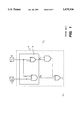
- FIG. 1 shows a part Y of a one-bit adder. It produces an output-carry bit C 1 from input data bits a 1 and b 1 and an input-carry bit C 2 .
- the logic that produces the output sum bit of the adder is not shown in the figure.
- the logic product (AND) of the input data bits is called the generate bit G, and the logic sum (OR) of the input data bits is called the propagate bit P.
- FIG. 2 shows a schematic diagram of a part of a four-bit ripple adder.
- Each rectangular box Y with a dashed outline can be substituted by the dashed box Y in FIG. 1.
- the output sum bits are again not shown in the Figure.
- the most significant bit is represented by the smallest subscript, whereas the least significant bit is represented by the largest subscript.
- the input-carry bit C 4 has to ripple through each one-bit adder; this rippling process delays the response time of the circuit.
- FIG. 3 shows part of a two-bit carry-lookahead adder (logic that produces the sum bits has been omitted). Each box marked X can be substituted by the box X in FIG. 1.
- the present invention provides a computer-aided method that reduces the complexity of designing carry-lookahead adders.
- the computer implements the adder automatically from two entered numbers that capture the essence of a design.
- carry-lookahead adders had to be redesigned manually in the gate level to test different ideas.
- this invention one only needs to change the two numbers and the carry-lookahead adders are automatically redesigned by the computer.
- the carry-lookahead adder in the invention is of the kind that adds two binary numbers and an input-carry bit.
- a length number and a blocks-in-group number are entered into a computer by a user.
- the computer responding to the length-number, automatically designs a first structure with a plurality of logic blocks. Each such block has a circuit to receive one bit from each binary number and to produce a propagate and a generate bit.
- the computer responding to the blocks-in-group number, the computer automatically designs a second structure by arranging the preceding-level logic blocks into one or more groups. Each group has the specified blocks-in-groups number of preceding-level logic blocks, except that one group may have less than the number of blocks if there are not enough blocks. Then the computer creates a next-level logic block for each group. Each next-level logic block has a logic circuit that receives the propagate and generate bits from all the blocks in a group of preceding-level logic blocks. Each next-level logic block also produces a propagate bit PLp and a generate bit GLp. If the number of logic blocks designed in the preceding step has more than one block, the computer automatically repeats the design process from the step of "arranging the preceding-level logic blocks into one or more groups" until the number of logic blocks designed in the preceding step is one.
- the computer formulates a final logic circuit to produce an output-carry bit of the adder from the input-carry bit and from the propagate PLp and generate GLp bits formed in the preceding step.
- the output-carry bit is equal to (the Propagate bit PLp * the input-carry bit + the Generate bit GLp).
- the output carry bit of the adder is formed by operating in parallel on the bits in the binary numbers.
- the computer receives a length number and a blocks-in-group number entered by a user. Then the computer generates the first and the second structures as in the first embodiment except that the condition controlling the termination of the design process is different. The design process is repeated if the number of next-level logic blocks designed is more than the blocks-in-group number. If the number of next-level logic blocks is not more than the blocks-in-group number, then the logic blocks designed in the preceding step are joined sequentially.
- the first logic block in the joint sequence receives the input-carry bit of the adder. Every logic block sequentially generates a carry bit that is received by its immediately next logic block and that is equal to (its PLp * its received carry bit + its GLp). The carry bit generated by the last logic block in the sequence is an output-carry bit of the adder.
- the computer automatically formulates the logic circuits to generate the output-carry bit of the carry-lookahead adder.
- the numbers are entered into the computer in any convenient way, for example, through a text editor or a graphical editor.
- FIG. 1 shows a part of a one-bit adder in the prior art.
- FIG. 2 shows a part of a four-bit ripple adder in the prior art.
- FIG. 3 shows a part of a two-bit carry-lookahead adder in the prior art.
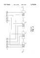
- FIG. 4 shows a part of a three-bit carry-lookahead adder in the prior art.
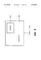
- FIG. 5 illustrates a computer that has incorporated the computer-aided method in the present invention.
- FIG. 6 shows a flow-chart illustrating a first preferred embodiment of the present invention.
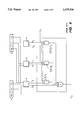
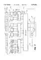
- FIG. 7 shows a representation of an eight-bit carry-lookahead adder designed by the first preferred embodiment of the invention.
- FIG. 8 illustrates a flow-chart illustrating a second preferred embodiment of the present invention.
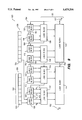
- FIG. 9 shows a representation of an eight-bit carry-lookahead adder designed by the second preferred embodiment of the invention.
- the present invention provides a computer-aided method of designing a carry-lookahead adder. With this method, a designer can easily design the adder by just entering two or more numbers into the computer that incorporates the computer-aided method. This is especially beneficial during a typical design process where a design has to be tuned to test different ideas.
- FIG. 5 shows a computer 300 with a memory 302 that has incorporated the computer-aided method.
- a user 304 enters two or more numbers into the computer 300, and a carry-lookahead adder is automatically designed.
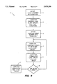
- FIG. 6 shows a flow-chart illustrating the steps in a first preferred embodiment of the present invention for designing a carry-lookahead adder of the kind that adds two binary numbers and an input-carry bit.
- FIG. 7 illustrates a representation of an eight-bit carry-lookahead adder designed by the first preferred embodiment of the invention.
- a length-number is entered (step 1) into the computer by a user.
- the number specifies the length in bits, 27, of the binary numbers 40 and 42 to be added; in the example shown in FIG. 7, the length-number is 8 because each input number has 8 bits.
- the computer responding to the length-number entered, automatically designs (step 2) a first structure 50, with a plurality of logic blocks, such as 10 through 24.
- the computer formulates a logic circuit to receive one bit from each binary number; for example, block 22 receives bits 32 and 44.
- Each block also produces two bits, a propagate bit and a generate bit; for example, the block 22 produces the propagate bit 26 and the generate bit 28.
- the propagate bit is the logic sum of the received bits of that block, and the generate bit is the logic product of the received bits of that block.
- a blocks-in-group number is entered (step 3) into the computer by a user; in the example shown in FIG. 7, that number is 3.
- the computer responding to the blocks-in-group number, automatically provides a second structure 51 which arranges the preceding-level logic blocks into one or more groups (step 4), such as blocks 10, 12 and 14 are arranged into one group.
- Each group has the specified blocks-in-group number of blocks, except for one group which may have less than that number of blocks if there are not enough blocks.
- blocks 22 and 24 are arranged in a group with less than the blocks-in-group number of blocks.
- next-level logic block 30 receives the propagate and generate bits from blocks 22 and 24. From the received bits, the logic circuit produces a propagate PLp and a generate GLp bit as follows:
- P0 to Pn-1 are the received propagate bits; and G0 to Gn-1 are the received generate bits.
- the computer uses standard circuit techniques to generate the logic circuit; for example, an AND gate with the required number of inputs to produce the bit PLp.
- next-level logic blocks designed in the preceding step If the number of next-level logic blocks designed in the preceding step is more than one, the computer automatically repeats from step four until the number of logic blocks designed in its preceding step is one (step 6). In the example shown in FIG. 7, three next-level logic blocks are created, namely 29, 30 and 31. The number of logic blocks created is more than one, so the computer automatically repeats from step 4 to create another level of logic blocks. After this level of logic block is created, the repeating process stops because this level has just one block 64.
- a final logic circuit 56 is created (step 7) using the input-carry bit 58, the propagate PLp and generate GLp bits produced by the preceding level 54.
- the final logic circuit produces the output-carry bit 62 of the adder 20 as follows:
- One preferred position to produce the sum bits of the adder is in the logic blocks of the first structure 50. This is achieved by first coupling the input carry bit from the final logic circuit 56 to its preceding-level logic block 64. Then a carry bit created by each logic block in the second structure 51 is coupled to each of its corresponding preceding-level-logic blocks; for example, the block 64 produces a carry bit 57 for block 30.
- the block 64 has three preceding-level logic blocks 29, 30 and 31, so it creates three carry bits and couples one to each preceding-level logic block. If the three carry bits are C0, C1 and C2, then their equations as follows:
- P2-P0 are the received propagate bits
- G2-G0 are the received generate bits by block 64.
- a carry bit is created by each logic block in the second structure 51 and coupled to each of its corresponding preceding-level logic blocks. This leads to every logic block in the first structure 50 receiving a carry bit from a logic block in the second structure 51; for example, the logic block 22 receives a carry bit 34 from the logic block 30. Each logic block in the first structure produces a sum bit; for example, the logic block 22 receives a carry bit 34 and produces a sum bit 23.
- the equation defining a sum bit for each logic block in the first structure is as follows:
- two numbers are entered into the computer, a length number and a blocks-in-group number.
- the block-in-group number is used to arrange preceding-level logic blocks into one or more groups.
- a list of blocks-in-group numbers are entered into the computer. The numbers are used to arrange preceding-level logic blocks into many groups. Each group has one of the entered blocks-in-group numbers of blocks.
- the list of numbers for the first level 52 is (3, 3, 2)--indicating that the first group has three blocks, the second group has three blocks and the third has two.
- the list of number for the second level is just (3). So, the total list of numbers, called size-lists-of-lists, to be entered into the computer is ((3, 3, 2), (3)).
- the computer formulates the logic circuits to produce the sum bits together with the output-carry bit of the carry-lookahead adder.
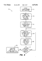
- FIG. 8 shows a flow-chart illustrating the steps in the second preferred embodiment of the present invention for designing a carry-lookahead adder of the kind that adds two binary numbers 126 and 128, and an input-carry bit 137.
- FIG. 9 shows a representation of an eight-bit carry-lookahead adder 100 designed by the second preferred embodiment of the invention.
- a user enters two numbers into the computer, a length-number and a blocks-in-group number.
- the length number, 27, specifying the length in bits, 102, of the binary numbers to be added is entered into the computer (step 77); in the example shown in FIG. 9, the length-number is 8 because each input number has 8 bits.
- the computer responding to the length-number entered, automatically designs (step 79) a first structure 104, with logic blocks 106 through 120. For each logic block, the computer formulates a logic circuit to receive one bit from each binary number; for example, the block 106 receives bits 122 and 124 from the binary numbers 126 and 128 respectively.
- Each block also produces two bits, a propagate bit and a generate bit; for example, the block 106 produces the propagate bit 130 and the generate bit 132.
- the propagate bit is the logic sum of the received bits of that block
- the generate bit is the logic product of the received bits of that block.
- the second number, the blocks-in-group number being entered into the computer is 2.
- the computer responding to the blocks-in-group number automatically provides a second structure 125 which arranges the preceding-level 104 logic blocks into one or more groups (step 83).
- the preceding-level blocks 106 and 108 are arranged into one group.
- Each group has the specified blocks-in-group number of blocks, except for one group which may have less than that number of blocks if there are not enough blocks.
- the computer automatically creates a next-level logic block for each group, and formulates for each logic block a logic circuit.
- the logic circuit receives the propagate and generate bits from all of the blocks in one of the groups of preceding-level logic blocks.
- the computer creates the next-level logic blocks 132, 134, 136 and 138.
- the next-level logic block 132 receives the propagate bits 130 and 142 and the generate bits 132 and 140 from the preceding-level logic blocks 106 and 108.
- each logic circuit produces a propagate PLp bit as in equation 1, and a generate GLp bit as in equation 2.
- the logic circuit in the logic block 132 generates bits as follows:
- step 87 the computer automatically repeats from the step of "arranging the preceding-level logic blocks into one or more groups" (step 83) until the number of logic blocks designed in its preceding step is not more than the blocks-in-group number.
- the number of logic blocks designed in the preceding step is 4 which is more than the blocks-in-group number 2.
- the computer then automatically arranges the 4 preceding-level logic blocks into 2 groups and creates two next-level logic blocks 144 and 146. In this level, there are only two blocks which is not more than the blocks-in-group. The computer proceeds into the final step.
- the computer sequentially joins together the one or more logic blocks in the preceding level; for example, blocks 144 and 146 are sequentially joined together.
- the first block 146 in the sequence receives the input-carry bit 137 of the carry-lookahead adder 100. Every logic block in the final level sequentially generates a carry bit that is coupled to its immediately next logic block; for example, the logic block 146 generates a carry bit 150 which is received by its immediately next logic block 144. Then the next logic block 144 generates a carry bit 152.
- the carry bit generated by each logic block is equal to (its produced propagate bit PLp * its received carry bit + its produced generate bit GLp).
- the carry bit generated by the last logic block 144 in the final level is the output carry bit 152 of the adder 100.
- two numbers, the length number and the blocks-in-group number are entered into the computer.
- the blocks-in-group number is used to arrange preceding-level logic blocks into one or more groups.
- a list of blocks-in-group numbers is entered into the computer. The numbers are used to arrange preceding-level logic blocks into many groups.
- Each group uses one of the entered blocks-in-group numbers to specify the number of preceding-level logic blocks in the group. One or more levels of logic blocks are then formed until all the entered blocks-in-group numbers are used. If the number of logic blocks designed in the preceding step has used up all the entered numbers, then the computer, 89, joins sequentially the logic blocks designed in the preceding step.
- the list of numbers for the first level in the second structure is (2, 2, 2, 2)--indicating each group has two blocks.
- the list of number for the second level is (2, 2).
- the total list of numbers, called size-lists-of-lists to be entered into the computer is ((2, 2, 2, 2), (2, 2)).
- the computer formulates the logic circuits for the output-carry bit 142 of the carry-lookahead adder 100.
- the logic circuits of the carry-lookahead adder can be tuned by changing the numbers entered into the computer, which is done in any convenient way, for example, through a text editor or through a graphical editor.
- FIG. 9 illustrates one way to formulate the sum in the logic blocks in the first structure 104.
- the input-carry bit 137 is fed into the logic block 120, which with its received bits from the binary numbers 126 and 128, forms a sum bit and a carry bit 154.
- One way to generate the logic circuit for the carry bit 154 is as shown in FIG. 1; and one way to generate the sum bit is as shown in equation 3 and 4.
- the carry bit 154 is received by the next logic block 118 to generate its sum bit and carry bit. While ripple adding is being done, the carry bit 156 from the logic block 118 is generated in parallel by the logic block 138 in the first level of the second structure. Similarly, the carry bit 151 for the block 112 in the first structure 104 is generated in parallel by the logic block 146 in the second structure 125.
- Every type of circuit can be represented by a few essential parameters in a computer. By entering the few parameters in the computer, a user designs and tunes the circuit.
Abstract
Description
PLp=P0 * P1 * . . . * P(n-1); (1)
GLp=G0+(G1 * P0)+(G2* P0 * P1)+ . . . +(G(n-1) * P0 * . . . * P(n-2));(2)
C0=(PLp * input-carry bit)+GLp.
Half-sum=XOR(its received bits from the 2 binary numbers); (3)
Sum bit=XOR(its received carry bit, half-sum); (4)
PLp=P0*P1; and
GLp=G0+G1*P0.
Claims (5)
G0+(G1 * P0)+(G2 * P0 * P1)+. . . +(G(n-1) * P0 * . . . * P(n-2)),
G0+(G1 * P0)+(G2 * P0 * P1)+. . . +(G(n-1) * P0 * . . . * P(n-2)),
Priority Applications (4)
| Application Number | Priority Date | Filing Date | Title |
|---|---|---|---|
| US08/031,775 US5479356A (en) | 1990-10-18 | 1993-03-15 | Computer-aided method of designing a carry-lookahead adder |
| GB9404738A GB2276256A (en) | 1993-03-15 | 1994-03-10 | A computer-aided method of designing a carry-lookahead adder. |
| DE4408789A DE4408789A1 (en) | 1993-03-15 | 1994-03-15 | A computer-aided method for constructing an adder with anticipatory carry-over |
| JP6043577A JPH06324845A (en) | 1993-03-15 | 1994-03-15 | Computer-aided designing method of carry look-ahead adder |
Applications Claiming Priority (2)
| Application Number | Priority Date | Filing Date | Title |
|---|---|---|---|
| US59996790A | 1990-10-18 | 1990-10-18 | |
| US08/031,775 US5479356A (en) | 1990-10-18 | 1993-03-15 | Computer-aided method of designing a carry-lookahead adder |
Related Parent Applications (1)
| Application Number | Title | Priority Date | Filing Date |
|---|---|---|---|
| US59996790A Continuation-In-Part | 1990-10-18 | 1990-10-18 |
Publications (1)
| Publication Number | Publication Date |
|---|---|
| US5479356A true US5479356A (en) | 1995-12-26 |
Family
ID=21861322
Family Applications (1)
| Application Number | Title | Priority Date | Filing Date |
|---|---|---|---|
| US08/031,775 Expired - Lifetime US5479356A (en) | 1990-10-18 | 1993-03-15 | Computer-aided method of designing a carry-lookahead adder |
Country Status (4)
| Country | Link |
|---|---|
| US (1) | US5479356A (en) |
| JP (1) | JPH06324845A (en) |
| DE (1) | DE4408789A1 (en) |
| GB (1) | GB2276256A (en) |
Cited By (5)
| Publication number | Priority date | Publication date | Assignee | Title |
|---|---|---|---|---|
| US5812521A (en) * | 1996-07-01 | 1998-09-22 | International Business Machines Corporation | Static adder using BICMOS emitter dot circuits |
| US5944777A (en) * | 1997-05-05 | 1999-08-31 | Intel Corporation | Method and apparatus for generating carries in an adder circuit |
| US6438572B1 (en) * | 1998-09-21 | 2002-08-20 | Rn2R, L.L.C. | Adder having reduced number of internal layers and method of operation thereof |
| US6539413B1 (en) * | 2000-03-15 | 2003-03-25 | Agere Systems Inc. | Prefix tree adder with efficient sum generation |
| US7444366B2 (en) | 2000-02-18 | 2008-10-28 | Hewlett-Packard Development Company, L.P. | Faster shift value calculation using modified carry-lookahead adder |
Citations (7)
| Publication number | Priority date | Publication date | Assignee | Title |
|---|---|---|---|---|
| EP0104845A2 (en) * | 1982-09-25 | 1984-04-04 | Kabushiki Kaisha Toshiba | Process control apparatus |
| WO1985001807A1 (en) * | 1983-10-14 | 1985-04-25 | Ford Motor Company | Selective parametric self-calibrating control system |
| US4639854A (en) * | 1983-02-01 | 1987-01-27 | Sanyo Denki Co. Ltd. | High gain feedback control system |
| US4730266A (en) * | 1984-02-09 | 1988-03-08 | U.S. Philips Corporation | Logic full adder circuit |
| WO1991000568A1 (en) * | 1989-06-23 | 1991-01-10 | Vlsi Technology, Inc. | Conditional-sum carry structure compiler |
| US5095458A (en) * | 1990-04-02 | 1992-03-10 | Advanced Micro Devices, Inc. | Radix 4 carry lookahead tree and redundant cell therefor |
| US5377122A (en) * | 1989-09-05 | 1994-12-27 | Lsi Logic Corporation | Logic compiler for design of circuit models |
-
1993
- 1993-03-15 US US08/031,775 patent/US5479356A/en not_active Expired - Lifetime
-
1994
- 1994-03-10 GB GB9404738A patent/GB2276256A/en not_active Withdrawn
- 1994-03-15 JP JP6043577A patent/JPH06324845A/en active Pending
- 1994-03-15 DE DE4408789A patent/DE4408789A1/en not_active Ceased
Patent Citations (8)
| Publication number | Priority date | Publication date | Assignee | Title |
|---|---|---|---|---|
| EP0104845A2 (en) * | 1982-09-25 | 1984-04-04 | Kabushiki Kaisha Toshiba | Process control apparatus |
| US4639854A (en) * | 1983-02-01 | 1987-01-27 | Sanyo Denki Co. Ltd. | High gain feedback control system |
| WO1985001807A1 (en) * | 1983-10-14 | 1985-04-25 | Ford Motor Company | Selective parametric self-calibrating control system |
| US4730266A (en) * | 1984-02-09 | 1988-03-08 | U.S. Philips Corporation | Logic full adder circuit |
| WO1991000568A1 (en) * | 1989-06-23 | 1991-01-10 | Vlsi Technology, Inc. | Conditional-sum carry structure compiler |
| US5126965A (en) * | 1989-06-23 | 1992-06-30 | Vlsi Technology, Inc. | Conditional-sum carry structure compiler |
| US5377122A (en) * | 1989-09-05 | 1994-12-27 | Lsi Logic Corporation | Logic compiler for design of circuit models |
| US5095458A (en) * | 1990-04-02 | 1992-03-10 | Advanced Micro Devices, Inc. | Radix 4 carry lookahead tree and redundant cell therefor |
Non-Patent Citations (8)
| Title |
|---|
| John P. Fishburn, "A Depth-Decreasing Heuristic for Combinational Logic or How to Convert a Ripple-Carry Adder into a Carry-Lookahead Adder or Anything In-Between", 27th ACM/IEEE Design Automation Conference, 1990, pp. 361-364. |
| John P. Fishburn, A Depth Decreasing Heuristic for Combinational Logic or How to Convert a Ripple Carry Adder into a Carry Lookahead Adder or Anything In Between , 27th ACM/IEEE Design Automation Conference, 1990, pp. 361 364. * |
| M. E. David and C. W. Gwyn, "CAD Systems for IC Design", IEEE Transactions on CAD, vol. CAD-1, No. 1, Jan. 1982. |
| M. E. David and C. W. Gwyn, CAD Systems for IC Design , IEEE Transactions on CAD, vol. CAD 1, No. 1, Jan. 1982. * |
| Mekhallalati et al., "New Parallel Multiplier Design", Electronics Letters, 13th Aug. 1992, vol. 28, No. 17, pp. 1650-1651. |
| Mekhallalati et al., New Parallel Multiplier Design , Electronics Letters, 13th Aug. 1992, vol. 28, No. 17, pp. 1650 1651. * |
| Pak K. Chan et al., "Delay Optimization of Carry-Skip Adders and Block Carry-Lookahead Adders Using Multidimensional Dynamic Programming", IEEE Transactions on Computers, vol. 41, No. 8, Aug. 1992, pp. 920-930. |
| Pak K. Chan et al., Delay Optimization of Carry Skip Adders and Block Carry Lookahead Adders Using Multidimensional Dynamic Programming , IEEE Transactions on Computers, vol. 41, No. 8, Aug. 1992, pp. 920 930. * |
Cited By (5)
| Publication number | Priority date | Publication date | Assignee | Title |
|---|---|---|---|---|
| US5812521A (en) * | 1996-07-01 | 1998-09-22 | International Business Machines Corporation | Static adder using BICMOS emitter dot circuits |
| US5944777A (en) * | 1997-05-05 | 1999-08-31 | Intel Corporation | Method and apparatus for generating carries in an adder circuit |
| US6438572B1 (en) * | 1998-09-21 | 2002-08-20 | Rn2R, L.L.C. | Adder having reduced number of internal layers and method of operation thereof |
| US7444366B2 (en) | 2000-02-18 | 2008-10-28 | Hewlett-Packard Development Company, L.P. | Faster shift value calculation using modified carry-lookahead adder |
| US6539413B1 (en) * | 2000-03-15 | 2003-03-25 | Agere Systems Inc. | Prefix tree adder with efficient sum generation |
Also Published As
| Publication number | Publication date |
|---|---|
| JPH06324845A (en) | 1994-11-25 |
| GB9404738D0 (en) | 1994-04-27 |
| DE4408789A1 (en) | 1994-09-22 |
| GB2276256A (en) | 1994-09-21 |
Similar Documents
| Publication | Publication Date | Title |
|---|---|---|
| US4682303A (en) | Parallel binary adder | |
| US5040139A (en) | Transmission gate multiplexer (TGM) logic circuits and multiplier architectures | |
| EP0101318B1 (en) | Digital filters | |
| US5257218A (en) | Parallel carry and carry propagation generator apparatus for use with carry-look-ahead adders | |
| US6353919B2 (en) | Pass-transistor logic circuit and a method of designing thereof | |
| US5161119A (en) | Weighted-delay column adder and method of organizing same | |
| EP0146963A2 (en) | Iir digital filter | |
| US5122982A (en) | Carry generation method and apparatus | |
| US4138731A (en) | High speed binary and binary coded decimal adder | |
| US5479356A (en) | Computer-aided method of designing a carry-lookahead adder | |
| US5036483A (en) | Binary adding apparatus | |
| US4389723A (en) | High-speed pattern generator | |
| JPH0545982B2 (en) | ||
| US5047974A (en) | Cell based adder with tree structured carry, inverting logic and balanced loading | |
| JP3556950B2 (en) | Structure and method for reducing the number of carry look-ahead adder stages in high speed arithmetic devices | |
| US7024445B2 (en) | Method and apparatus for use in booth-encoded multiplication | |
| US4882698A (en) | Cell based ALU with tree structured carry, inverting logic and balanced loading | |
| US5586071A (en) | Enhanced fast multiplier | |
| US6003059A (en) | Carry select adder using two level selectors | |
| US5875125A (en) | X+2X adder with multi-bit generate/propagate circuit | |
| US5357457A (en) | Adder with carry look ahead circuit | |
| US4879675A (en) | Parity generator circuit and method | |
| US5424971A (en) | Unsigned constant multiplier compiler | |
| US5227678A (en) | Fast digital comparison circuit for fuzzy logic operations | |
| GB2197163A (en) | Pseudo-random noise code generating circuit |
Legal Events
| Date | Code | Title | Description |
|---|---|---|---|
| STPP | Information on status: patent application and granting procedure in general |
Free format text: APPLICATION UNDERGOING PREEXAM PROCESSING |
|
| AS | Assignment |
Owner name: HEWLEET-PACKARD COMPANY, CALIFORNIA Free format text: ASSIGNMENT OF ASSIGNORS INTEREST;ASSIGNORS:SHACKLEFORD, BARRY;CULBERTSON, BRUCE;REEL/FRAME:006712/0306 Effective date: 19930920 |
|
| FEPP | Fee payment procedure |
Free format text: PAYOR NUMBER ASSIGNED (ORIGINAL EVENT CODE: ASPN); ENTITY STATUS OF PATENT OWNER: LARGE ENTITY |
|
| FPAY | Fee payment |
Year of fee payment: 4 |
|
| AS | Assignment |
Owner name: HEWLETT-PACKARD COMPANY, COLORADO Free format text: MERGER;ASSIGNOR:HEWLETT-PACKARD COMPANY;REEL/FRAME:011523/0469 Effective date: 19980520 |
|
| FPAY | Fee payment |
Year of fee payment: 8 |
|
| FPAY | Fee payment |
Year of fee payment: 12 |
|
| AS | Assignment |
Owner name: SAMSUNG ELECTRONICS CO., LTD., KOREA, REPUBLIC OF Free format text: ASSIGNMENT OF ASSIGNORS INTEREST;ASSIGNORS:HEWLETT-PACKARD DEVELOPMENT COMPANY, L.P.;HEWLETT-PACKARD COMPANY;REEL/FRAME:026198/0139 Effective date: 20101019 |