US5436203A - Shielded liquid encapsulated semiconductor device and method for making the same - Google Patents
Shielded liquid encapsulated semiconductor device and method for making the same Download PDFInfo
- Publication number
- US5436203A US5436203A US08/270,602 US27060294A US5436203A US 5436203 A US5436203 A US 5436203A US 27060294 A US27060294 A US 27060294A US 5436203 A US5436203 A US 5436203A
- Authority
- US
- United States
- Prior art keywords
- encapsulant
- substrate
- conductive
- filling
- dammed area
- Prior art date
- Legal status (The legal status is an assumption and is not a legal conclusion. Google has not performed a legal analysis and makes no representation as to the accuracy of the status listed.)
- Expired - Lifetime
Links
Images

Classifications
-
- H10W76/47—
-
- H10W42/20—
-
- H10W42/276—
-
- H10W74/117—
-
- H10W74/121—
-
- H10W90/701—
-
- H10W72/5449—
-
- H10W72/884—
-
- H10W72/932—
-
- H10W74/00—
-
- H10W90/734—
-
- H10W90/754—
-
- Y—GENERAL TAGGING OF NEW TECHNOLOGICAL DEVELOPMENTS; GENERAL TAGGING OF CROSS-SECTIONAL TECHNOLOGIES SPANNING OVER SEVERAL SECTIONS OF THE IPC; TECHNICAL SUBJECTS COVERED BY FORMER USPC CROSS-REFERENCE ART COLLECTIONS [XRACs] AND DIGESTS
- Y10—TECHNICAL SUBJECTS COVERED BY FORMER USPC
- Y10T—TECHNICAL SUBJECTS COVERED BY FORMER US CLASSIFICATION
- Y10T29/00—Metal working
- Y10T29/49—Method of mechanical manufacture
- Y10T29/49002—Electrical device making
- Y10T29/49117—Conductor or circuit manufacturing
- Y10T29/49124—On flat or curved insulated base, e.g., printed circuit, etc.
- Y10T29/4913—Assembling to base an electrical component, e.g., capacitor, etc.
- Y10T29/49146—Assembling to base an electrical component, e.g., capacitor, etc. with encapsulating, e.g., potting, etc.
Definitions
- the present invention relates to a commonly assigned, co-pending patent application by Leo M. Higgins et al. entitled, "Shielded Electronic Component Assembly and Method for Making the Same," Ser. No. 08/229,495, filed Apr. 19, 1994.
- the present invention relates generally to semiconductor devices and more specifically to semiconductor devices which are shielded from electromagnetic interference (EMI).
- EMI electromagnetic interference
- EMI electromagnetic interference
- One of the most typical methods for shielding semiconductor devices from EMI is to include a grounded metal cap or cover surrounding those devices within a system that may be susceptible to EMI interference.
- metal caps are certainly effective in shielding EMI, use of such caps have several drawbacks. For instance, the final system layout size may be constrained from further reductions due to the presence of such metal caps.
- Another drawback is that metal caps can interfere with forced air system cooling. The presence of a metal cap over a semiconductor device prevents air from reaching an internal device which may be dissipating heat within the system.
- a manufacturing disadvantage associated with using metal caps is that a metal cap is a separate piece part. Preferably the number of piece parts within a manufacturing process is kept to a minimum to avoid unnecessary handling costs and assembly operations. Moreover, the use of a separate metal cap requires an additional processing step of soldering the metal cap to a reference or ground plane.
- a semiconductor device is made by providing a circuitized substrate having a first surface, an internal conductive reference plane, and a conductive member on the first surface which is electrically coupled to the reference plane.
- a semiconductor die is mounted to the first surface of the substrate, and is electrically connected to the circuitized substrate.
- a first dam is provided on the first surface of the substrate, and surrounds the semiconductor die to form a first dammed area, such that the conductive member on the first surface of the substrate is beyond the first dammed area.
- the first dammed area is filled with a first encapsulant which is an electrically insulative liquid encapsulant which encapsulates the die.
- a second dam is provided on the first surface of the substrate and surrounds the first dammed area to form a second dammed area.
- the conductive member on the first surface of the substrate is within the second dammed area.
- the second dammed area is then filled with a second encapsulant which is an electrically conductive liquid encapsulant.
- the second encapsulant encapsulates the first encapsulant and is an electrical contact with the conductive member.
- Another form of the invention includes a semiconductor device made by such a process.
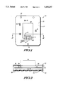
- FIG. 1 is a top down view of a circuitized substrate suitable for use in accordance with the present invention.
- FIG. 2 is a cross-sectional illustration of the substrate of FIG. 1, taken along the line 2--2.
- FIG. 3 is a top down view of the substrate of FIG. 1 after a semiconductor die and first and second dams have been formed on the substrate in accordance with the present invention.
- FIG. 4 is a cross-sectional illustration of the substrate, die, and dams of FIG. 3 taken along the line 4--4, after first and second liquid encapsulants have been dispensed in accordance with an embodiment of the present invention.
- the present invention establishes an EMI shielded device without use of a separate metal cover or cap, thereby reducing the device profile and mass as compared to prior art shielded devices.
- a semiconductor die is mounted to a circuitized substrate, such as a printed circuit board.
- the die is electrically connected to the circuitized substrate in any conventional manner.
- the die is then covered by dispensing a first liquid encapsulant material over the die.
- the first liquid encapsulant covering the die is constrained by a first dam formed on the substrate which surrounds the die.
- This first encapsulant is an electrically insulative encapsulating material, such as an epoxy-based or silicon-based resin used in conventional "glob top" applications.
- a second liquid encapsulant is dispensed over the first encapsulant.
- the second encapsulant is an electrically conductive encapsulant, such as an epoxy-based or silicon-based resin having conductive (e.g. metal) filler particles.
- the second encapsulant covers the first encapsulant and is electrically connected to a conductive member on the circuitized substrate which is electrically connected to a voltage reference plane, such as an internal ground plane of the substrate. Together the voltage reference plane and the conductive second encapsulant effectively sandwich the semiconductor die between grounded elements, thereby effectively shielding the die from EMI both internal and external to the system.
- FIG. 1 is a top down view of a circuitized substrate 12 suitable for use in accordance with practicing the present invention.
- FIG. 2 is a cross-sectional illustration of substrate 12 taken along the line 2--2 of FIG. 1.
- substrate 12 is an epoxy-glass based printed circuit board, made from, for instance, FR4 or bismaleimide-triazine resin.
- Substrate 12 has a top surface 13 and a bottom surface 14. Formed on each surface are various conductive patterns.
- top surface 13 includes a plurality of conductive traces 15 and a plurality of bonding posts 16.
- top surface 13 Also included on top surface 13 is one or more conductive reference pads 18.
- the conductive traces 15 and reference pads 18 are routed to either an internal conductive plane or to bottom surface 14 by a plurality of conductive vias 20. More specifically, reference pads 18 are routed to an internal reference plane 22 within substrate 12, while conductive traces 15 are routed to a plurality of conductive pads 24 formed on bottom surface 14.
- internal reference plane 22 In order to route individual signals or traces from the top surface 13 to the bottom surface 14, it may be necessary to somehow pass through internal reference plane 22. This may be accomplished by forming perforations in reference plane 22, and extending a conductive via through the perforation while maintaining electrical isolation.
- Those connections to the die which will be tied to the reference plane can be tied directly to the reference plane by a conductive via without the use of perforations. Routing of the various conductive elements vertically through substrate 12 is achieved through the use of conductive vias 20, while routing of conductive members horizontally over surfaces of substrate 12 is accomplished by conductive traces. For example, on the bottom surface 14 of the substrate, a particular conductive via may be routed to a specific conductive pad 24 by a conductive trace (not shown), similar to conductive traces 15 illustrated on top surface 13. Substrate 12 may also include features to aid in manufacturing, such as strip alignment holes 25.
- Substrate 12 is manufactured in accordance with conventional processes.
- each of the planar conductive elements such as traces 15, bonding posts 16, reference pads 18, reference plane 22, and conductive pads 24, may be formed by laminating or depositing a metal material (e.g. copper) onto a base insulating substrate material. Subsequent lithographic and etching techniques are then used to define the actual conductive patterns.
- a multi-layer substrate such as that illustrated in FIGS. 1 and 2 which includes at least one internal conductive plane, two or more insulating layers must be laminated together to form the completed substrate. Such techniques are well known in the art.
- conductive vias may be formed by drilling holes through the insulating material, and subsequently depositing or plating metal into the holes, either along the sidewalls of the holes or throughout the holes such that the holes become filled.
- formation of conductive vias in multi-layer epoxy-glass substrate materials is well understood within the art.
- substrate 12 also includes a layer of solder resist 26.
- Solder resist is a layer which is laminated or screen printed onto substrate 12, and serves to mask or shield conductive members on top and bottom surfaces 13 and 14, respectively, from subsequent soldering and/or plating operations. Solder resists materials are commercially available for this purpose.
- solder resist 26 masks all portions of the surface except portions of conductive pads 24 to which conductive terminals, such as solder balls, are subsequently attached. Thus, any conductive traces which may have been on bottom surface 14 are masked by solder resist 26.
- solder resist 26 covers all portions of the surface except a die receiving area 28 and conductive reference pads 18. Any conductive elements within die receiving area 28 thus remain exposed, as do portions of reference pads 18, after application of solder resist 26 to the top surface 13.
- FIG. 3 is a top down illustration demonstrating how substrate 12 may be used in accordance with the present invention to form a semiconductor device.
- FIG. 4 is a cross-sectional illustration of a finished ball grid array semiconductor device 30 as it would appear taken along the line 4--4 through substrate 12 illustrated in FIG. 3.
- a semiconductor die 32 is mounted to top surface 13 of substrate 12 within die receiving area 28.
- Semiconductor die 32 may be any type of integrated circuit including, but not limited to, a memory device, a microprocessor, a microcontroller, an analog device, a digital signal processor, or the like. Die 32 is attached to substrate 12 by conventional means, such as by an epoxy die attach material 34.
- device 30 is a ball grid array device, wherein the external terminals are in the form of a plurality of conductive solder balls 38. It should be noted that as illustrated in FIG.
- FIG. 4 does not illustrate how wire bonds 36 are directly electrically coupled to any conductive pads 24 and solder balls 38; however, such connections are well within the knowledge of one of ordinary skill in the art.
- semiconductor die 32 is encapsulated by a first liquid encapsulant 38.
- encapsulant 38 is an epoxy-based or silicon-based resin which is dispensed in a liquid form, such as those resins used in "glob top" encapsulation of semiconductor devices.
- a dam structure 40 is first formed on substrate 12 around die receiving area 28. Dam structure 40 is used to constrain the flow of liquid encapsulant 38 during dispense. In accordance with the present invention, dam structure 40 is formed around the die receiving area 28, and without encompassing reference pads 18, thus preventing liquid encapsulant 38 from encapsulating the reference pads.
- the dam structure may either be formed on the solder resist or within the opening in solder resist, both alternatives being illustrated in FIGS. 3 and 4.
- Dam structure 40 is preferably formed by dispensing a material similar to that of liquid encapsulant 38 using a syringe to define the dam shape.
- the difference between the materials used to form dam structure 40 and in liquid encapsulant 38 is viscosity of the materials.
- Encapsulant 38 provides environmental protection for semiconductor die 32. This protection includes protection against moisture or contaminant ingress as well as against mechanical damage. So that device 30 may function electrically, encapsulant 38 is an electrically insulating material to prevent electrical short circuiting of the individual wire bond and conductive traces. As with conventional liquid resin encapsulants, encapsulant 38 may also include filler particles, such as silica, silicon dioxide, silicon nitride, or the like, which serve to control flow characteristics and thermal expansion properties of the material.
- encapsulant 42 is an epoxy-based or silicon-based resin having conductive filler particles dispersed throughout.
- the purpose of having conductive filler particles is to establish electrical conductivity of encapsulant 42, thereby enabling encapsulant 42 to be electrically tied to internal reference plane 22 by reference pads 18 and conductive vias 20.
- the precursor material used for encapsulant 42 is the same or very similar to the material used for encapsulant 38 because it is desirable to have the physical properties of the two materials as similar as possible to avoid interface discontinuities.
- the same resin precursor may be used in both first encapsulant 38 and second encapsulant 42; the only difference being the type and amount of filler particles used in the two encapsulants. Thus, upon curing the resins of the two encapsulants merge so that a distinct interface does not exist.
- Suitable filler particles in encapsulant 42 to establish electrical conductivity include metal particles or conductively coated polymer particles of sufficient concentration to establish electrical conductivity throughout the encapsulant. Fillers made from silver, copper, palladium, and gold are all suitable for practicing the invention.
- dam structure 44 is preferably an epoxy-based or silicon-based resin of sufficient viscosity to maintain the dam structure and constrain the flow of encapsulant 42.
- the dam structure Upon curing, the dam structure preferably becomes as similar to encapsulant 42 as possible; however, dam structure 44 need not be (but may be) electrically conductive.
- Curing encapsulant 42 may be performed after first encapsulant 38 has been cured, but preferably to avoid unnecessary process steps all encapsulant materials are cured at the same time.
- Device 30 has many advantages over prior art shielded devices. As is evident from the illustration of FIG. 4, semiconductor die 32 is effectively shielded from both the top and bottom by the combination of electrically conductive encapsulant 42 and internal reference plane 22. In device operation, internal reference plane 22 will be tied to a constant voltage potential, such as ground potential, thereby establishing a shield surrounding semiconductor die 32 which protects against either external or internal EMI. Moreover, device 30 does not have many of the disadvantages associated with using a separate metal cap to provide the EMI shielding. Specifically, device 30 does not require handling or use of a separate piece part which reduces device, handling, and general manufacturing costs. Instead, a liquid encapsulant is used to provide the shielding.
- Dam structures 40 and 44 and encapsulant 38 and encapsulant 42 may be formed on substrate 12 within the same processing step (encapsulation), although formed in a sequential fashion. There is no need to have intermediate curing cycles between the dispense of encapsulant 38 and the dispense of encapsulant 42, provided the set time of encapsulant 38 is sufficiently short so that encapsulant 42 may be dispensed on encapsulant 38, prior to cure, without excessive mixing of the materials.
- Another advantage of the present invention over the use of metal caps for shielding is the elimination of any air gaps between the encapsulation of the semiconductor die and the shield.
- a metal cap In using a metal cap, there is inherently an air gap in-between the encapsulation material and the metal shield. This air gap hinders thermal dissipation from the device, as well as hinders any forced air cooling which may be present within the system.
- a device in accordance with the present invention has no such air gap. Rather encapsulant 42 is an intimate contact with encapsulant 38, and upon curing the two materials may merge to the extent that there is not an abrupt interface which may impede thermal dissipation.
- An additional thermal advantage of a device formed in accordance with the present invention is that there is an inherent thermal path away from semiconductor die 32.
- encapsulant 42 may also serve as an alpha particle protection layer for memory devices as well as an EMI shield.
- the thickness, density, and types of filler particles used in encapsulant 42 may be chosen to protect against a particular range of impinging alpha particle energies.
- the fillers chosen for alpha particle protection may be conductive, thereby also allowing encapsulant 42 to serve as an EMI shield.
- electrically insulative filler particles for alpha particle protection may be combined with conductive fillers in the outermost encapsulant.
- Another advantageous aspect of the present invention is that the use of an additional encapsulant 42 may be used to compensate for stresses between substrate 12 and first encapsulant 38. In prior art device thermal expansion coefficient mismatch between encapsulating materials and substrate materials can lead to warpage of the substrate.
- the second encapsulate can be formulated to compensate or offset these differentials. For example, if first encapsulant 38 is a tensile encapsulate, the second encapsulant 42 may be made to be compressive, or vice versa.
- Such compensation is preferably accomplished through choice of filler materials and amount of filler used in each encapsulant, rather than by modifications to the precursor resin components of the encapsulants.
- the base resins preferably remain similar so that a distinct interface between the two encapsulants is substantially avoided upon curing.
- solder resist be absent from the die receiving area of the substrate.
- the presence of solder resist within the die receiving area is possible provided that appropriate electrical connections can be made to the conductive elements of the substrate.
- fillers used in the outer most encapsulant may be chosen to protect against impinging alpha particles, whether conductive or not.
- carbon black powder can be added to encapsulant to enhance thermal conductivity and to modify the color and contrast of the encapsulant for marking and cosmetic purposes. Therefore, it is intended that this invention encompass all such variations and modifications as fall within the scope of the appended claims.
Landscapes
- Structures Or Materials For Encapsulating Or Coating Semiconductor Devices Or Solid State Devices (AREA)
Abstract
Description
Claims (12)
Priority Applications (1)
| Application Number | Priority Date | Filing Date | Title |
|---|---|---|---|
| US08/270,602 US5436203A (en) | 1994-07-05 | 1994-07-05 | Shielded liquid encapsulated semiconductor device and method for making the same |
Applications Claiming Priority (1)
| Application Number | Priority Date | Filing Date | Title |
|---|---|---|---|
| US08/270,602 US5436203A (en) | 1994-07-05 | 1994-07-05 | Shielded liquid encapsulated semiconductor device and method for making the same |
Publications (1)
| Publication Number | Publication Date |
|---|---|
| US5436203A true US5436203A (en) | 1995-07-25 |
Family
ID=23031997
Family Applications (1)
| Application Number | Title | Priority Date | Filing Date |
|---|---|---|---|
| US08/270,602 Expired - Lifetime US5436203A (en) | 1994-07-05 | 1994-07-05 | Shielded liquid encapsulated semiconductor device and method for making the same |
Country Status (1)
| Country | Link |
|---|---|
| US (1) | US5436203A (en) |
Cited By (155)
| Publication number | Priority date | Publication date | Assignee | Title |
|---|---|---|---|---|
| US5654243A (en) * | 1993-11-18 | 1997-08-05 | Fujitsu Limited | Process for fabricating a semiconductor device in a resin package housed in a frame having high conductivity |
| WO1997039482A1 (en) * | 1996-04-18 | 1997-10-23 | Tessera, Inc. | Methods for manufacturing a semiconductor package |
| US5696031A (en) * | 1996-11-20 | 1997-12-09 | Micron Technology, Inc. | Device and method for stacking wire-bonded integrated circuit dice on flip-chip bonded integrated circuit dice |
| US5756380A (en) * | 1995-11-02 | 1998-05-26 | Motorola, Inc. | Method for making a moisture resistant semiconductor device having an organic substrate |
| US5784260A (en) * | 1996-05-29 | 1998-07-21 | International Business Machines Corporation | Structure for constraining the flow of encapsulant applied to an I/C chip on a substrate |
| US5796586A (en) * | 1996-08-26 | 1998-08-18 | National Semiconductor, Inc. | Substrate board having an anti-adhesive solder mask |
| US5866953A (en) * | 1996-05-24 | 1999-02-02 | Micron Technology, Inc. | Packaged die on PCB with heat sink encapsulant |
| WO1998050949A3 (en) * | 1997-05-07 | 1999-02-04 | Lsi Logic Corp | Pbga stiffener package and method of manufacturing |
| US5888850A (en) * | 1997-09-29 | 1999-03-30 | International Business Machines Corporation | Method for providing a protective coating and electronic package utilizing same |
| US5892660A (en) * | 1996-08-29 | 1999-04-06 | Micron Technology, Inc. | Single in line memory module adapter |
| US5894167A (en) * | 1996-05-08 | 1999-04-13 | Micron Technology, Inc. | Encapsulant dam standoff for shell-enclosed die assemblies |
| US5950074A (en) * | 1997-04-18 | 1999-09-07 | Amkor Technology, Inc. | Method of making an integrated circuit package |
| US5962810A (en) * | 1997-09-09 | 1999-10-05 | Amkor Technology, Inc. | Integrated circuit package employing a transparent encapsulant |
| US5981314A (en) * | 1996-10-31 | 1999-11-09 | Amkor Technology, Inc. | Near chip size integrated circuit package |
| US5989942A (en) * | 1994-11-24 | 1999-11-23 | Dow Corning Toray Silicone Co., Ltd. | Method for fabricating semiconductor device |
| WO1999062119A1 (en) * | 1998-05-22 | 1999-12-02 | Amkor Technology, Inc. | Rf shielded electronic device |
| US5998867A (en) * | 1996-02-23 | 1999-12-07 | Honeywell Inc. | Radiation enhanced chip encapsulant |
| WO1999063632A1 (en) * | 1998-06-03 | 1999-12-09 | Federal-Mogul Corporation | Backplate assembly with seal |
| WO2000013233A1 (en) * | 1998-08-28 | 2000-03-09 | Amkor Technology, Inc. | Electromagnetic interference shield device and method |
| US6052045A (en) * | 1999-03-12 | 2000-04-18 | Kearney-National, Inc. | Electromechanical switching device package with controlled impedance environment |
| US6067709A (en) * | 1996-02-23 | 2000-05-30 | Mpm Corporation | Applying encapsulating material to substrates |
| US6071139A (en) * | 1998-03-31 | 2000-06-06 | Micron Technology, Inc. | Locking assembly for securing semiconductor device to carrier substrate |
| US6117797A (en) * | 1998-09-03 | 2000-09-12 | Micron Technology, Inc. | Attachment method for heat sinks and devices involving removal of misplaced encapsulant |
| US6117705A (en) * | 1997-04-18 | 2000-09-12 | Amkor Technology, Inc. | Method of making integrated circuit package having adhesive bead supporting planar lid above planar substrate |
| US6132543A (en) * | 1997-03-14 | 2000-10-17 | Matsushita Electric Industrial Co., Ltd. | Method of manufacturing a packaging substrate |
| US6150726A (en) * | 1996-09-06 | 2000-11-21 | International Business Machines Corp. | Component carrier with raised bonding sites |
| US6163956A (en) * | 1998-02-23 | 2000-12-26 | Micron Technology, Inc. | Method of making chip scale package with heat spreade |
| US6229209B1 (en) | 1995-02-23 | 2001-05-08 | Matsushita Electric Industrial Co., Ltd. | Chip carrier |
| EP0917189A4 (en) * | 1996-07-23 | 2001-07-04 | Seiko Epson Corp | METHOD FOR MOUNTING AN ENCAPSULATED BODY ON AN OPTICAL BOARD AND CONVERTER |
| US6274927B1 (en) | 1999-06-03 | 2001-08-14 | Amkor Technology, Inc. | Plastic package for an optical integrated circuit device and method of making |
| US6297548B1 (en) | 1998-06-30 | 2001-10-02 | Micron Technology, Inc. | Stackable ceramic FBGA for high thermal applications |
| US6297960B1 (en) | 1998-06-30 | 2001-10-02 | Micron Technology, Inc. | Heat sink with alignment and retaining features |
| US6299463B1 (en) | 1997-06-06 | 2001-10-09 | Micron Technology, Inc. | Device and method for electrically or thermally coupling to the backsides of integrated circuit dice in chip-on-board applications |
| US6326687B1 (en) | 1998-09-01 | 2001-12-04 | Micron Technology, Inc. | IC package with dual heat spreaders |
| WO2002017394A1 (en) * | 2000-08-22 | 2002-02-28 | Conexant Systems, Inc. | Molded shield structures and method for their fabrication |
| US20020045290A1 (en) * | 1996-02-20 | 2002-04-18 | Michael B. Ball | Flip chip and conventional stack |
| US20020053452A1 (en) * | 1996-09-04 | 2002-05-09 | Quan Son Ky | Semiconductor package and method therefor |
| US6398573B1 (en) | 1998-03-31 | 2002-06-04 | Micron Technology, Inc. | Locking assembly for securing semiconductor device to carrier substrate |
| US6444499B1 (en) * | 2000-03-30 | 2002-09-03 | Amkor Technology, Inc. | Method for fabricating a snapable multi-package array substrate, snapable multi-package array and snapable packaged electronic components |
| US6444501B1 (en) * | 2001-06-12 | 2002-09-03 | Micron Technology, Inc. | Two stage transfer molding method to encapsulate MMC module |
| US6448635B1 (en) | 1999-08-30 | 2002-09-10 | Amkor Technology, Inc. | Surface acoustical wave flip chip |
| US6452278B1 (en) | 2000-06-30 | 2002-09-17 | Amkor Technology, Inc. | Low profile package for plural semiconductor dies |
| US6459144B1 (en) * | 2001-03-02 | 2002-10-01 | Siliconware Precision Industries Co., Ltd. | Flip chip semiconductor package |
| US6459145B1 (en) * | 1995-10-24 | 2002-10-01 | Oki Electric Industry Co., Ltd. | Semiconductor device having an improved structure for preventing cracks, and improved small-sized semiconductor |
| EP1251566A1 (en) * | 2001-04-19 | 2002-10-23 | United Test Center Inc. | Low profile optically-sensitive semiconductor package |
| US6479901B1 (en) * | 1998-12-21 | 2002-11-12 | Oki Electric Industry Co., Ltd. | Semiconductor device having interconnected external electrode pads and wire bonding pads |
| US20020168798A1 (en) * | 1996-10-31 | 2002-11-14 | Glenn Thomas P. | Method of making near chip size integrated circuit package |
| US20020185712A1 (en) * | 2001-06-08 | 2002-12-12 | Brian Stark | Circuit encapsulation technique utilizing electroplating |
| US6512680B2 (en) * | 1997-09-19 | 2003-01-28 | Canon Kabushiki Kaisha | Semiconductor package |
| US20030038376A1 (en) * | 2001-08-21 | 2003-02-27 | Bolken Todd O. | Semiconductor die packages with standard ball grid array footprint and method for assembling the same |
| US20030080402A1 (en) * | 1998-02-23 | 2003-05-01 | Corisis David J. | Chip scale package with heat spreader and method of manufacture |
| WO2003012867A3 (en) * | 2001-08-01 | 2003-05-22 | Ibm | Emi shielding for electronic packages |
| US6583444B2 (en) | 1997-02-18 | 2003-06-24 | Tessera, Inc. | Semiconductor packages having light-sensitive chips |
| US6608390B2 (en) | 2001-11-13 | 2003-08-19 | Kulicke & Soffa Investments, Inc. | Wirebonded semiconductor package structure and method of manufacture |
| US6614102B1 (en) | 2001-05-04 | 2003-09-02 | Amkor Technology, Inc. | Shielded semiconductor leadframe package |
| US20030169138A1 (en) * | 2002-03-08 | 2003-09-11 | Motta James J. | Surface mount molded relay package and method of manufacturing same |
| US20030192716A1 (en) * | 2002-04-10 | 2003-10-16 | Atsushi Yamaguchi | Printed circuit board having through-hole protected by barrier and method of manufacturing the same |
| US6657294B2 (en) * | 2000-05-23 | 2003-12-02 | Koninklijke Philips Electronics N.V. | Data carrier having an IC module with a protection mechanism for protecting the parts of the IC module from mechanical stress |
| US6664613B2 (en) * | 2000-08-31 | 2003-12-16 | Micron Technology, Inc. | Magnetic shielding for integrated circuits |
| USRE38381E1 (en) | 2000-07-21 | 2004-01-13 | Kearney-National Inc. | Inverted board mounted electromechanical device |
| US20040007771A1 (en) * | 1999-08-24 | 2004-01-15 | Amkor Technology, Inc. | Semiconductor package and method for fabricating the smae |
| US20040056277A1 (en) * | 2002-09-17 | 2004-03-25 | Chippac, Inc. | Semiconductor multi-package module including stacked-die package and having wire bond interconnect between stacked packages |
| US20040061213A1 (en) * | 2002-09-17 | 2004-04-01 | Chippac, Inc. | Semiconductor multi-package module having package stacked over die-up flip chip ball grid array package and having wire bond interconnect between stacked packages |
| US20040063246A1 (en) * | 2002-09-17 | 2004-04-01 | Chippac, Inc. | Semiconductor multi-package module having package stacked over die-down flip chip ball grid array package and having wire bond interconnect between stacked packages |
| US20040063242A1 (en) * | 2002-09-17 | 2004-04-01 | Chippac, Inc. | Semiconductor multi-package module having package stacked over ball grid array package and having wire bond interconnect between stacked packages |
| US20040061212A1 (en) * | 2002-09-17 | 2004-04-01 | Chippac, Inc. | Semiconductor multi-package module having wire bond interconnect between stacked packages |
| US20040065963A1 (en) * | 2002-09-17 | 2004-04-08 | Chippac, Inc. | Semiconductor multi-package module having wire bond interconnect between stacked packages and having electrical shield |
| US20040087057A1 (en) * | 2002-10-30 | 2004-05-06 | Advanpack Solutions Pte. Ltd. | Method for fabricating a flip chip package with pillar bump and no flow underfill |
| US20040089922A1 (en) * | 2002-11-08 | 2004-05-13 | Gerber Mark A. | Semiconductor device and method therefor |
| US6750533B2 (en) * | 2002-04-10 | 2004-06-15 | Siliconware Precision Industries Co., Ltd. | Substrate with dam bar structure for smooth flow of encapsulating resin |
| US6759307B1 (en) * | 2000-09-21 | 2004-07-06 | Micron Technology, Inc. | Method to prevent die attach adhesive contamination in stacked chips |
| US20040150085A1 (en) * | 1996-12-03 | 2004-08-05 | Oki Electric Industry Co., Ltd. | Semiconductor device having a chip-size package |
| US6784534B1 (en) | 2002-02-06 | 2004-08-31 | Amkor Technology, Inc. | Thin integrated circuit package having an optically transparent window |
| US20040178483A1 (en) * | 2003-03-12 | 2004-09-16 | Cheng-Ho Hsu | Method of packaging a quad flat no-lead semiconductor and a quad flat no-lead semiconductor |
| US20040211591A1 (en) * | 1998-01-27 | 2004-10-28 | Hitachi Cable Ltd. | Wiring board, semiconductor device, electronic device, and circuit board for electronic parts |
| US6821821B2 (en) | 1996-04-18 | 2004-11-23 | Tessera, Inc. | Methods for manufacturing resistors using a sacrificial layer |
| US20040266068A1 (en) * | 2003-06-30 | 2004-12-30 | Matayabas J. Christopher | Wire-bonded package with electrically insulating wire encapsulant and thermally conductive overmold |
| US6861720B1 (en) | 2001-08-29 | 2005-03-01 | Amkor Technology, Inc. | Placement template and method for placing optical dies |
| US20050074923A1 (en) * | 2003-10-03 | 2005-04-07 | Vahid Goudarzi | Metallic dam and method of forming therefor |
| US20050082088A1 (en) * | 2002-12-23 | 2005-04-21 | Weston Roth | Apparatus and method for improving coupling across plane discontinuities on circuit boards |
| US20050133916A1 (en) * | 2003-12-17 | 2005-06-23 | Stats Chippac, Inc | Multiple chip package module having inverted package stacked over die |
| US20050140005A1 (en) * | 2003-12-31 | 2005-06-30 | Advanced Semiconductor Engineering Inc. | Chip package structure |
| US20050148160A1 (en) * | 2002-03-06 | 2005-07-07 | Farnworth Warren M. | Encapsulated semiconductor components and methods of fabrication |
| US20050269676A1 (en) * | 2004-05-24 | 2005-12-08 | Chippac, Inc | Adhesive/spacer island structure for stacking over wire bonded die |
| US20050275081A1 (en) * | 2004-06-12 | 2005-12-15 | Roger Chang | Embedded chip semiconductor having dual electronic connection faces |
| US20050287714A1 (en) * | 2004-06-29 | 2005-12-29 | Michael Walk | Enhancing epoxy strength using kaolin filler |
| US20060001158A1 (en) * | 2004-06-30 | 2006-01-05 | Matayabas James C Jr | Package stress management |
| US20060012018A1 (en) * | 2004-07-13 | 2006-01-19 | Chippac, Inc. | Semiconductor multipackage module including die and inverted land grid array package stacked over ball grid array package |
| US20060018098A1 (en) * | 2004-07-22 | 2006-01-26 | Adrian Hill | PCB board incorporating thermo-encapsulant for providing controlled heat dissipation and electromagnetic functions and associated method of manufacturing a PCB board |
| US20060097404A1 (en) * | 2004-11-11 | 2006-05-11 | Byeong-Yeon Cho | Semiconductor package with conductive molding compound and manufacturing method thereof |
| US20060220210A1 (en) * | 2005-03-31 | 2006-10-05 | Stats Chippac Ltd. | Semiconductor assembly including chip scale package and second substrate and having exposed substrate surfaces on upper and lower sides |
| US20060220209A1 (en) * | 2005-03-31 | 2006-10-05 | Stats Chippac Ltd. | Semiconductor stacked package assembly having exposed substrate surfaces on upper and lower sides |
| US20060244117A1 (en) * | 2005-04-29 | 2006-11-02 | Stats Chippac, Ltd. | Semiconductor package including second substrate and having exposed substrate surfaces on upper and lower sides |
| US20060249851A1 (en) * | 2005-05-05 | 2006-11-09 | Stats Chippac Ltd. | Multiple Chip Package Module Including Die Stacked Over Encapsulated Package |
| US7148529B2 (en) * | 2001-03-30 | 2006-12-12 | Kabushiki Kaisha Toshiba | Semiconductor package |
| US20060284299A1 (en) * | 2005-06-20 | 2006-12-21 | Stats Chippac Ltd. | Module Having Stacked Chip Scale Semiconductor Packages |
| US20070015314A1 (en) * | 2004-05-24 | 2007-01-18 | Chippac, Inc | Adhesive/Spacer Island Structure for Multiple Die Package |
| US20070018296A1 (en) * | 2004-05-24 | 2007-01-25 | Chippac, Inc | Stacked Semiconductor Package having Adhesive/Spacer Structure and Insulation |
| US20070111388A1 (en) * | 2002-10-08 | 2007-05-17 | Chippac, Inc. | Semiconductor Multi-Package Module Having Inverted Second Package Stacked Over Die-Up Flip-Chip Ball Grid Array (BGA) Package |
| US20070158833A1 (en) * | 2006-01-04 | 2007-07-12 | Soo-San Park | Integrated circuit package system including stacked die |
| US20070158809A1 (en) * | 2006-01-04 | 2007-07-12 | Chow Seng G | Multi-chip package system |
| US20070182018A1 (en) * | 2006-02-09 | 2007-08-09 | Stats Chippac Ltd. | Integrated circuit package system including zero fillet resin |
| US20070185973A1 (en) * | 2006-02-07 | 2007-08-09 | Dot Hill Systems, Corp. | Pull data replication model |
| US20070190690A1 (en) * | 2006-02-14 | 2007-08-16 | Stats Chippac Ltd. | Integrated circuit package system with exposed interconnects |
| US20070187136A1 (en) * | 2004-09-29 | 2007-08-16 | Masahiro Higashiguchi | Printed circuit board, method of producing the same, and electronic unit |
| US20080227302A1 (en) * | 2007-03-12 | 2008-09-18 | Honeywell International Inc. | Fibrous laminate interface for security coatings |
| US20080224322A1 (en) * | 2007-03-15 | 2008-09-18 | Sanyo Electric Co., Ltd. | Semiconductor device and manufacturing method thereof |
| US20080237892A1 (en) * | 2007-03-30 | 2008-10-02 | Oki Electric Industry Co., Ltd. | Semiconductor device |
| US20080277151A1 (en) * | 2007-05-08 | 2008-11-13 | Occam Portfolio Llc | Electronic Assemblies without Solder and Methods for their Manufacture |
| US20080289867A1 (en) * | 1994-12-05 | 2008-11-27 | Freescale Semiconductor, Inc. | Multi-strand substrate for ball-grid array assemblies and method |
| US20080303136A1 (en) * | 2007-06-08 | 2008-12-11 | Nec Corporation | Semiconductor device and method for manufacturing same |
| US20090000114A1 (en) * | 2007-06-27 | 2009-01-01 | Rf Micro Devices, Inc. | Heat sink formed with conformal shield |
| US20090001606A1 (en) * | 2007-06-27 | 2009-01-01 | Shinko Electric Industries Co., Ltd. | Semiconductor package and semiconductor device using the same |
| US20090027863A1 (en) * | 2003-04-04 | 2009-01-29 | Marcos Karnezos | Method for making a semiconductor multipackage module including a processor and memory package assemblies |
| US20090267171A1 (en) * | 2008-04-24 | 2009-10-29 | Micron Technology, Inc. | Pre-encapsulated cavity interposer |
| US20100001388A1 (en) * | 2007-03-23 | 2010-01-07 | Fujitsu Limited | Electronic device, electronic apparatus mounted with electronic device, article equipped with electronic device and method of producing electronic device |
| US7687315B2 (en) | 2005-04-29 | 2010-03-30 | Stats Chippac Ltd. | Stacked integrated circuit package system and method of manufacture therefor |
| US20100118482A1 (en) * | 2008-11-13 | 2010-05-13 | Mosaid Technologies Incorporated | System including a plurality of encapsulated semiconductor chips |
| US20100187557A1 (en) * | 2009-01-28 | 2010-07-29 | Samoilov Arkadii V | Light Sensor Using Wafer-Level Packaging |
| US7855100B2 (en) | 2005-03-31 | 2010-12-21 | Stats Chippac Ltd. | Integrated circuit package system with an encapsulant cavity and method of fabrication thereof |
| US20110074037A1 (en) * | 2009-09-29 | 2011-03-31 | Elpida Memory, Inc. | Semiconductor device |
| US20110210436A1 (en) * | 2010-02-26 | 2011-09-01 | Seng Guan Chow | Integrated circuit packaging system with encapsulation and method of manufacture thereof |
| US20120018858A1 (en) * | 2010-07-21 | 2012-01-26 | Freescale Semiconductor, Inc. | Method of assembling integrated circuit device |
| US20120187583A1 (en) * | 2009-12-23 | 2012-07-26 | Intel Corporation | Methods and apparatuses to stiffen integrated circuit package |
| US20120326339A1 (en) * | 2011-06-24 | 2012-12-27 | Kabushiki Kaisha Toshiba | Semiconductor device, and method and apparatus for manufacturing the same |
| US8349659B1 (en) | 2007-06-25 | 2013-01-08 | Rf Micro Devices, Inc. | Integrated shield for a no-lead semiconductor device package |
| US20130059402A1 (en) * | 2010-02-22 | 2013-03-07 | Andreas Jakob | Method and A System for Producing a Semi-Conductor Module |
| US20130148401A1 (en) * | 2011-12-07 | 2013-06-13 | Apple Inc. | Systems and methods for stacked semiconductor memory devices |
| FR2986902A1 (en) * | 2012-02-09 | 2013-08-16 | Pixinbio | Assembling module of analysis device of biological sample, comprises applying external formwork to upper face, and coating conductor by encapsulation material to deposit material in cavity delimited by internal wall of external formwork |
| US8835226B2 (en) | 2011-02-25 | 2014-09-16 | Rf Micro Devices, Inc. | Connection using conductive vias |
| TWI469301B (en) * | 2002-09-17 | 2015-01-11 | 恰巴克有限公司 | Semiconductor multi-package module with wire contact interconnection in stacked package |
| US8959762B2 (en) | 2005-08-08 | 2015-02-24 | Rf Micro Devices, Inc. | Method of manufacturing an electronic module |
| US9137934B2 (en) | 2010-08-18 | 2015-09-15 | Rf Micro Devices, Inc. | Compartmentalized shielding of selected components |
| US20160262292A1 (en) * | 2015-03-06 | 2016-09-08 | Samsung Electronics Co., Ltd. | Circuit element package, manufacturing method thereof, and manufacturing apparatus thereof |
| US9627230B2 (en) | 2011-02-28 | 2017-04-18 | Qorvo Us, Inc. | Methods of forming a microshield on standard QFN package |
| US9807890B2 (en) | 2013-05-31 | 2017-10-31 | Qorvo Us, Inc. | Electronic modules having grounded electromagnetic shields |
| US20170325365A1 (en) | 2016-05-04 | 2017-11-09 | Samsung Electronics Co., Ltd. | Hollow shielding structure for different types of circuit elements and manufacturing method thereof |
| US20180040568A1 (en) * | 2016-08-05 | 2018-02-08 | Siliconware Precision Industries Co., Ltd. | Electronic package and method for fabricating the same |
| US10201072B2 (en) * | 2016-12-12 | 2019-02-05 | Samsung Electronics Co., Ltd. | EMI shielding structure and manufacturing method thereof |
| US20190164807A1 (en) * | 2017-11-27 | 2019-05-30 | Texas Instruments Incorporated | Electronic package for integrated circuits and related methods |
| US10477687B2 (en) | 2016-08-04 | 2019-11-12 | Samsung Electronics Co., Ltd. | Manufacturing method for EMI shielding structure |
| US10531599B2 (en) | 2017-09-08 | 2020-01-07 | Samsung Electronics Co., Ltd. | Electromagnetic interference shielding structure |
| US10594020B2 (en) | 2017-07-19 | 2020-03-17 | Samsung Electronics Co., Ltd. | Electronic device having antenna element and method for manufacturing the same |
| CN111384033A (en) * | 2018-12-27 | 2020-07-07 | 南亚科技股份有限公司 | Semiconductor structure and method of making the same |
| US20210066228A1 (en) * | 2019-08-30 | 2021-03-04 | Advanced Semiconductor Engineering, Inc. | Package structure and method for manufacturing the same |
| US11058038B2 (en) | 2018-06-28 | 2021-07-06 | Qorvo Us, Inc. | Electromagnetic shields for sub-modules |
| US11114363B2 (en) | 2018-12-20 | 2021-09-07 | Qorvo Us, Inc. | Electronic package arrangements and related methods |
| US11127689B2 (en) | 2018-06-01 | 2021-09-21 | Qorvo Us, Inc. | Segmented shielding using wirebonds |
| US11264334B2 (en) | 2018-12-27 | 2022-03-01 | Nanya Technology Corporation | Package device and method of manufacturing the same |
| US11498831B2 (en) | 2016-01-13 | 2022-11-15 | Texas Instruments Incorporated | Structures for packaging stress-sensitive micro-electro-mechanical system stacked onto electronic circuit chip |
| US11515282B2 (en) | 2019-05-21 | 2022-11-29 | Qorvo Us, Inc. | Electromagnetic shields with bonding wires for sub-modules |
| US11538767B2 (en) | 2017-12-29 | 2022-12-27 | Texas Instruments Incorporated | Integrated circuit package with partitioning based on environmental sensitivity |
| WO2023007987A1 (en) * | 2021-07-29 | 2023-02-02 | 富士フイルム株式会社 | Electronic device and method for manufacturing same |
| US11817418B2 (en) * | 2019-11-25 | 2023-11-14 | Infineon Technologies Ag | Semiconductor device comprising a can housing a semiconductor die which is embedded by an encapsulant |
| US12417983B2 (en) * | 2022-09-08 | 2025-09-16 | Siliconware Precision Industries Co., Ltd. | Semiconductor package |
Citations (20)
| Publication number | Priority date | Publication date | Assignee | Title |
|---|---|---|---|---|
| US4218701A (en) * | 1978-07-24 | 1980-08-19 | Citizen Watch Co., Ltd. | Package for an integrated circuit having a container with support bars |
| US4264917A (en) * | 1978-10-19 | 1981-04-28 | Compagnie Internationale Pour L'informatique Cii-Honeywell Bull | Flat package for integrated circuit devices |
| US4477828A (en) * | 1982-10-12 | 1984-10-16 | Scherer Jeremy D | Microcircuit package and sealing method |
| US4707725A (en) * | 1985-09-30 | 1987-11-17 | Mitsubishi Denki Kabushiki Kaisha | Fluorescent coating for uv sensitive semiconductor device |
| US4758875A (en) * | 1981-04-30 | 1988-07-19 | Hitachi, Ltd. | Resin encapsulated semiconductor device |
| US4766095A (en) * | 1985-01-04 | 1988-08-23 | Oki Electric Industry Co., Ltd. | Method of manufacturing eprom device |
| US4768081A (en) * | 1984-11-17 | 1988-08-30 | Messerschmitt-Boelkow-Blohm Gmbh | Process for encapsulating microelectronic circuits with organic components |
| US4788583A (en) * | 1986-07-25 | 1988-11-29 | Fujitsu Limited | Semiconductor device and method of producing semiconductor device |
| US4843036A (en) * | 1987-06-29 | 1989-06-27 | Eastman Kodak Company | Method for encapsulating electronic devices |
| US4916522A (en) * | 1988-04-21 | 1990-04-10 | American Telephone And Telegraph Company , At & T Bell Laboratories | Integrated circuit package using plastic encapsulant |
| US4962415A (en) * | 1986-12-15 | 1990-10-09 | Hitachi Maxell, Ltd. | IC card |
| US5041395A (en) * | 1989-04-07 | 1991-08-20 | Sgs-Thomson Microelectronics S.A. | Method of encapsulating an integrated circuit using a punched metal grid attached to a perforated dielectric strip |
| US5087961A (en) * | 1987-01-28 | 1992-02-11 | Lsi Logic Corporation | Semiconductor device package |
| US5097317A (en) * | 1989-09-08 | 1992-03-17 | Mitsubishi Denki Kabushiki Kaisha | Resin-sealed semiconductor device |
| US5153379A (en) * | 1990-10-09 | 1992-10-06 | Motorola, Inc. | Shielded low-profile electronic component assembly |
| US5166772A (en) * | 1991-02-22 | 1992-11-24 | Motorola, Inc. | Transfer molded semiconductor device package with integral shield |
| US5206794A (en) * | 1991-12-20 | 1993-04-27 | Vlsi Technology, Inc. | Integrated circuit package with device and wire coat assembly |
| US5218234A (en) * | 1991-12-23 | 1993-06-08 | Motorola, Inc. | Semiconductor device with controlled spread polymeric underfill |
| US5258650A (en) * | 1991-08-26 | 1993-11-02 | Motorola, Inc. | Semiconductor device having encapsulation comprising of a thixotropic fluorosiloxane material |
| US5311060A (en) * | 1989-12-19 | 1994-05-10 | Lsi Logic Corporation | Heat sink for semiconductor device assembly |
-
1994
- 1994-07-05 US US08/270,602 patent/US5436203A/en not_active Expired - Lifetime
Patent Citations (20)
| Publication number | Priority date | Publication date | Assignee | Title |
|---|---|---|---|---|
| US4218701A (en) * | 1978-07-24 | 1980-08-19 | Citizen Watch Co., Ltd. | Package for an integrated circuit having a container with support bars |
| US4264917A (en) * | 1978-10-19 | 1981-04-28 | Compagnie Internationale Pour L'informatique Cii-Honeywell Bull | Flat package for integrated circuit devices |
| US4758875A (en) * | 1981-04-30 | 1988-07-19 | Hitachi, Ltd. | Resin encapsulated semiconductor device |
| US4477828A (en) * | 1982-10-12 | 1984-10-16 | Scherer Jeremy D | Microcircuit package and sealing method |
| US4768081A (en) * | 1984-11-17 | 1988-08-30 | Messerschmitt-Boelkow-Blohm Gmbh | Process for encapsulating microelectronic circuits with organic components |
| US4766095A (en) * | 1985-01-04 | 1988-08-23 | Oki Electric Industry Co., Ltd. | Method of manufacturing eprom device |
| US4707725A (en) * | 1985-09-30 | 1987-11-17 | Mitsubishi Denki Kabushiki Kaisha | Fluorescent coating for uv sensitive semiconductor device |
| US4788583A (en) * | 1986-07-25 | 1988-11-29 | Fujitsu Limited | Semiconductor device and method of producing semiconductor device |
| US4962415A (en) * | 1986-12-15 | 1990-10-09 | Hitachi Maxell, Ltd. | IC card |
| US5087961A (en) * | 1987-01-28 | 1992-02-11 | Lsi Logic Corporation | Semiconductor device package |
| US4843036A (en) * | 1987-06-29 | 1989-06-27 | Eastman Kodak Company | Method for encapsulating electronic devices |
| US4916522A (en) * | 1988-04-21 | 1990-04-10 | American Telephone And Telegraph Company , At & T Bell Laboratories | Integrated circuit package using plastic encapsulant |
| US5041395A (en) * | 1989-04-07 | 1991-08-20 | Sgs-Thomson Microelectronics S.A. | Method of encapsulating an integrated circuit using a punched metal grid attached to a perforated dielectric strip |
| US5097317A (en) * | 1989-09-08 | 1992-03-17 | Mitsubishi Denki Kabushiki Kaisha | Resin-sealed semiconductor device |
| US5311060A (en) * | 1989-12-19 | 1994-05-10 | Lsi Logic Corporation | Heat sink for semiconductor device assembly |
| US5153379A (en) * | 1990-10-09 | 1992-10-06 | Motorola, Inc. | Shielded low-profile electronic component assembly |
| US5166772A (en) * | 1991-02-22 | 1992-11-24 | Motorola, Inc. | Transfer molded semiconductor device package with integral shield |
| US5258650A (en) * | 1991-08-26 | 1993-11-02 | Motorola, Inc. | Semiconductor device having encapsulation comprising of a thixotropic fluorosiloxane material |
| US5206794A (en) * | 1991-12-20 | 1993-04-27 | Vlsi Technology, Inc. | Integrated circuit package with device and wire coat assembly |
| US5218234A (en) * | 1991-12-23 | 1993-06-08 | Motorola, Inc. | Semiconductor device with controlled spread polymeric underfill |
Non-Patent Citations (2)
| Title |
|---|
| Classen, et al; "Integrated Circuit Packages;" United States Statutory Invention Registration, No. H73, Filed Aug. 25, 1993, Appl. No. 526,413 and Published Jun. 3, 1986. |
| Classen, et al; Integrated Circuit Packages; United States Statutory Invention Registration, No. H73, Filed Aug. 25, 1993, Appl. No. 526,413 and Published Jun. 3, 1986. * |
Cited By (406)
| Publication number | Priority date | Publication date | Assignee | Title |
|---|---|---|---|---|
| US5654243A (en) * | 1993-11-18 | 1997-08-05 | Fujitsu Limited | Process for fabricating a semiconductor device in a resin package housed in a frame having high conductivity |
| US5989942A (en) * | 1994-11-24 | 1999-11-23 | Dow Corning Toray Silicone Co., Ltd. | Method for fabricating semiconductor device |
| US20080289867A1 (en) * | 1994-12-05 | 2008-11-27 | Freescale Semiconductor, Inc. | Multi-strand substrate for ball-grid array assemblies and method |
| US6229209B1 (en) | 1995-02-23 | 2001-05-08 | Matsushita Electric Industrial Co., Ltd. | Chip carrier |
| US6365499B1 (en) | 1995-02-23 | 2002-04-02 | Matsushita Electric Industrial Co., Ltd. | Chip carrier and method of manufacturing and mounting the same |
| US6372547B2 (en) * | 1995-02-23 | 2002-04-16 | Matsushita Electric Industrial Co., Ltd. | Method for manufacturing electronic device with resin layer between chip carrier and circuit wiring board |
| US6459145B1 (en) * | 1995-10-24 | 2002-10-01 | Oki Electric Industry Co., Ltd. | Semiconductor device having an improved structure for preventing cracks, and improved small-sized semiconductor |
| US5756380A (en) * | 1995-11-02 | 1998-05-26 | Motorola, Inc. | Method for making a moisture resistant semiconductor device having an organic substrate |
| US6140149A (en) * | 1996-02-20 | 2000-10-31 | Micron Technology, Inc. | Device and method for stacking wire-bonded integrated circuit dice on flip-chip bonded integrated circuit dice |
| US7166495B2 (en) | 1996-02-20 | 2007-01-23 | Micron Technology, Inc. | Method of fabricating a multi-die semiconductor package assembly |
| US20070117266A1 (en) * | 1996-02-20 | 2007-05-24 | Ball Michael B | Method of fabricating a multi-die semiconductor package assembly |
| US20020045290A1 (en) * | 1996-02-20 | 2002-04-18 | Michael B. Ball | Flip chip and conventional stack |
| US6067709A (en) * | 1996-02-23 | 2000-05-30 | Mpm Corporation | Applying encapsulating material to substrates |
| US5998867A (en) * | 1996-02-23 | 1999-12-07 | Honeywell Inc. | Radiation enhanced chip encapsulant |
| US6856235B2 (en) | 1996-04-18 | 2005-02-15 | Tessera, Inc. | Methods for manufacturing resistors using a sacrificial layer |
| US7091820B2 (en) | 1996-04-18 | 2006-08-15 | Tessera, Inc. | Methods for manufacturing resistors using a sacrificial layer |
| US7165316B2 (en) | 1996-04-18 | 2007-01-23 | Tessera, Inc. | Methods for manufacturing resistors using a sacrificial layer |
| US6294830B1 (en) | 1996-04-18 | 2001-09-25 | Tessera, Inc. | Microelectronic assembly with conductive terminals having an exposed surface through a dielectric layer |
| US6093584A (en) * | 1996-04-18 | 2000-07-25 | Tessera, Inc. | Method for encapsulating a semiconductor package having apertures through a sacrificial layer and contact pads |
| WO1997039482A1 (en) * | 1996-04-18 | 1997-10-23 | Tessera, Inc. | Methods for manufacturing a semiconductor package |
| US6821821B2 (en) | 1996-04-18 | 2004-11-23 | Tessera, Inc. | Methods for manufacturing resistors using a sacrificial layer |
| US6001671A (en) * | 1996-04-18 | 1999-12-14 | Tessera, Inc. | Methods for manufacturing a semiconductor package having a sacrificial layer |
| US20040233035A1 (en) * | 1996-04-18 | 2004-11-25 | Tessera, Inc. | Methods for manufacturing resistors using a sacrificial layer |
| US5895222A (en) * | 1996-05-08 | 1999-04-20 | Micron Technology, Inc. | Encapsulant dam standoff for shell-enclosed die assemblies |
| US5894167A (en) * | 1996-05-08 | 1999-04-13 | Micron Technology, Inc. | Encapsulant dam standoff for shell-enclosed die assemblies |
| US6617684B2 (en) | 1996-05-24 | 2003-09-09 | Micron Technology, Inc. | Packaged die on PCB with heat sink encapsulant |
| US5866953A (en) * | 1996-05-24 | 1999-02-02 | Micron Technology, Inc. | Packaged die on PCB with heat sink encapsulant |
| US6252308B1 (en) | 1996-05-24 | 2001-06-26 | Micron Technology, Inc. | Packaged die PCB with heat sink encapsulant |
| US20040036160A1 (en) * | 1996-05-24 | 2004-02-26 | Salman Akram | Packaged die on PCB with heat sink encapsulant and methods |
| US6853069B2 (en) | 1996-05-24 | 2005-02-08 | Micron Technology, Inc. | Packaged die on PCB with heat sink encapsulant and methods |
| US20070069372A1 (en) * | 1996-05-24 | 2007-03-29 | Salman Akram | Packaged die on PCB with heat sink encapsulant and methods |
| US20050189646A1 (en) * | 1996-05-24 | 2005-09-01 | Salman Akram | Packaged die on PCB with heat sink encapsulant and methods |
| US6534858B2 (en) | 1996-05-24 | 2003-03-18 | Micron Technology, Inc. | Assembly and methods for packaged die on pcb with heat sink encapsulant |
| US5784260A (en) * | 1996-05-29 | 1998-07-21 | International Business Machines Corporation | Structure for constraining the flow of encapsulant applied to an I/C chip on a substrate |
| EP0917189A4 (en) * | 1996-07-23 | 2001-07-04 | Seiko Epson Corp | METHOD FOR MOUNTING AN ENCAPSULATED BODY ON AN OPTICAL BOARD AND CONVERTER |
| US5796586A (en) * | 1996-08-26 | 1998-08-18 | National Semiconductor, Inc. | Substrate board having an anti-adhesive solder mask |
| DE19736139B4 (en) * | 1996-08-26 | 2004-07-15 | National Semiconductor Corp.(N.D.Ges.D.Staates Delaware), Santa Clara | circuit board |
| US6781848B2 (en) | 1996-08-29 | 2004-08-24 | Micron Technology, Inc. | Single-piece molded module housing |
| US5892660A (en) * | 1996-08-29 | 1999-04-06 | Micron Technology, Inc. | Single in line memory module adapter |
| US6233154B1 (en) | 1996-08-29 | 2001-05-15 | Micron Technology, Inc. | Single-piece molded module housing |
| US6570771B2 (en) | 1996-08-29 | 2003-05-27 | Micron Technology, Inc. | Single-piece molded module housing |
| US20030193788A1 (en) * | 1996-08-29 | 2003-10-16 | Farnworth Warren M. | Single-piece molded module housing |
| US20020053452A1 (en) * | 1996-09-04 | 2002-05-09 | Quan Son Ky | Semiconductor package and method therefor |
| US7927927B2 (en) | 1996-09-04 | 2011-04-19 | Freescale Semiconductor, Inc. | Semiconductor package and method therefor |
| US6150726A (en) * | 1996-09-06 | 2000-11-21 | International Business Machines Corp. | Component carrier with raised bonding sites |
| US6228676B1 (en) | 1996-10-31 | 2001-05-08 | Amkor Technology, Inc. | Near chip size integrated circuit package |
| US20020168798A1 (en) * | 1996-10-31 | 2002-11-14 | Glenn Thomas P. | Method of making near chip size integrated circuit package |
| US5981314A (en) * | 1996-10-31 | 1999-11-09 | Amkor Technology, Inc. | Near chip size integrated circuit package |
| US6150193A (en) * | 1996-10-31 | 2000-11-21 | Amkor Technology, Inc. | RF shielded device |
| US6962829B2 (en) | 1996-10-31 | 2005-11-08 | Amkor Technology, Inc. | Method of making near chip size integrated circuit package |
| US6071754A (en) * | 1996-11-20 | 2000-06-06 | Micron Technology, Inc. | Device and method for stacking wire-bonded integrated circuit dice on flip-chip bonded integrated circuit dice |
| US7423339B2 (en) | 1996-11-20 | 2008-09-09 | Mircon Technology, Inc. | Methods for stacking wire-bonded integrated circuit dice on flip-chip bonded integrated circuit dice |
| US20060033194A1 (en) * | 1996-11-20 | 2006-02-16 | Wark James M | Methods for stacking wire-bonded integrated circuit dice on flip-chip bonded integrated circuit dice |
| US7109059B2 (en) | 1996-11-20 | 2006-09-19 | Micron Technology, Inc. | Methods for stacking wire-bonded integrated circuit dice on flip-chip bonded integrated circuit dice |
| US20070063229A1 (en) * | 1996-11-20 | 2007-03-22 | Wark James M | Methods for stacking wire-bonded integrated circuit dice on flip-chip bonded integrated circuit dice |
| US20050161796A1 (en) * | 1996-11-20 | 2005-07-28 | Wark James M. | Methods for stacking wire-bonded integrated circuit dice on flip-chip bonded integrated circuit dice |
| US6869826B2 (en) | 1996-11-20 | 2005-03-22 | Micron Technology, Inc. | Methods for stacking wire-bonded integrated circuit dice on flip-chip bonded integrated circuit dice |
| US7282792B2 (en) | 1996-11-20 | 2007-10-16 | Micron Technology, Inc. | Methods for stacking wire-bonded integrated circuit dice on flip-chip bonded integrated circuit dice |
| US5696031A (en) * | 1996-11-20 | 1997-12-09 | Micron Technology, Inc. | Device and method for stacking wire-bonded integrated circuit dice on flip-chip bonded integrated circuit dice |
| US7402902B2 (en) | 1996-11-20 | 2008-07-22 | Micron Technology, Inc. | Methods for stacking wire-bonded integrated circuit dice on flip-chip bonded integrated circuit dice |
| US20070063328A1 (en) * | 1996-11-20 | 2007-03-22 | Wark James M | Methods for stacking wire-bonded integrated circuit dice on flip-chip bonded integrated circuit dice |
| US7411286B2 (en) | 1996-11-20 | 2008-08-12 | Micron Technology, Inc. | Methods for stacking wire-bonded integrated circuit dice on flip-chip bonded integrated circuit dice |
| US6399416B1 (en) | 1996-11-20 | 2002-06-04 | Micron Technology, Inc. | Device and method for stacking wire-bonded integrated circuit dice on flip-chip bonded integrated circuit dice |
| US20070063327A1 (en) * | 1996-11-20 | 2007-03-22 | Wark James M | Methods for stacking wire-bonded integrated circuit dice on flip-chip bonded integrated circuit dice |
| US7423338B2 (en) | 1996-11-20 | 2008-09-09 | Micron Technology, Inc. | Methods for stacking wire-bonded integrated circuit dice on flip-chip bonded integrated circuit dice |
| US20080311702A1 (en) * | 1996-11-20 | 2008-12-18 | Micron Technology, Inc. | Methods for stacking wire-bonded integrated circuit dice on flip-chip bonded integrated circuit dice |
| US20080315435A1 (en) * | 1996-11-20 | 2008-12-25 | Micron Technology, Inc. | Methods for stacking wire-bonded integrated circuit dice on flip-chip bonded integrated circuit dice |
| US6605489B2 (en) | 1996-11-20 | 2003-08-12 | Micron Technology, Inc. | Methods for stacking wire-bonded integrated circuit dice on flip-chip bonded integrated circuit dice |
| US20070063326A1 (en) * | 1996-11-20 | 2007-03-22 | Wark James M | Methods for stacking wire-bonded integrated circuit dice on flip-chip bonded integrated circuit dice |
| US7812436B2 (en) | 1996-11-20 | 2010-10-12 | Micron Technology, Inc. | Methods for stacking wire-bonded integrated circuit dice on flip-chip bonded integrated circuit dice |
| US20040029315A1 (en) * | 1996-11-20 | 2004-02-12 | Wark James M. | Methods for stacking wire-bonded integrated circuit dice on flip-chip bonded integrated circuit dice |
| US5973403A (en) * | 1996-11-20 | 1999-10-26 | Micron Technology, Inc. | Device and method for stacking wire-bonded integrated circuit dice on flip-chip bonded integrated circuit dice |
| US7776652B2 (en) | 1996-11-20 | 2010-08-17 | Micron Technology, Inc. | Methods for stacking wire-bonded integrated circuit dice on flip-chip bonded integrated circuit dice |
| US20090146287A1 (en) * | 1996-12-03 | 2009-06-11 | Oki Electric Industry Co., Ltd. | Semiconductor device having a chip-size package |
| US20040150085A1 (en) * | 1996-12-03 | 2004-08-05 | Oki Electric Industry Co., Ltd. | Semiconductor device having a chip-size package |
| US8154124B2 (en) | 1996-12-03 | 2012-04-10 | Oki Electric Industry Co., Ltd. | Semiconductor device having a chip-size package |
| US7335970B2 (en) * | 1996-12-03 | 2008-02-26 | Oki Electric Industry Co., Ltd. | Semiconductor device having a chip-size package |
| US7095054B2 (en) | 1997-02-18 | 2006-08-22 | Tessera, Inc. | Semiconductor package having light sensitive chips |
| US20030136968A1 (en) * | 1997-02-18 | 2003-07-24 | Tessera, Inc. | Semiconductor package having light sensitive chips |
| US6583444B2 (en) | 1997-02-18 | 2003-06-24 | Tessera, Inc. | Semiconductor packages having light-sensitive chips |
| US6888168B2 (en) | 1997-02-18 | 2005-05-03 | Tessera, Inc. | Semiconductor package having light sensitive chips |
| US20050035357A1 (en) * | 1997-02-18 | 2005-02-17 | Tessera, Inc. | Semiconductor package having light sensitive chips |
| US6132543A (en) * | 1997-03-14 | 2000-10-17 | Matsushita Electric Industrial Co., Ltd. | Method of manufacturing a packaging substrate |
| US7358445B1 (en) | 1997-03-14 | 2008-04-15 | Matsushita Electric Industrial Co., Ltd. | Circuit substrate and apparatus including the circuit substrate |
| US6034429A (en) * | 1997-04-18 | 2000-03-07 | Amkor Technology, Inc. | Integrated circuit package |
| US6268654B1 (en) | 1997-04-18 | 2001-07-31 | Ankor Technology, Inc. | Integrated circuit package having adhesive bead supporting planar lid above planar substrate |
| US5950074A (en) * | 1997-04-18 | 1999-09-07 | Amkor Technology, Inc. | Method of making an integrated circuit package |
| US6117705A (en) * | 1997-04-18 | 2000-09-12 | Amkor Technology, Inc. | Method of making integrated circuit package having adhesive bead supporting planar lid above planar substrate |
| US5972738A (en) * | 1997-05-07 | 1999-10-26 | Lsi Logic Corporation | PBGA stiffener package |
| WO1998050949A3 (en) * | 1997-05-07 | 1999-02-04 | Lsi Logic Corp | Pbga stiffener package and method of manufacturing |
| US6339256B2 (en) * | 1997-06-06 | 2002-01-15 | Micron Technology, Inc. | Device and method for electrically or thermally coupling to the backsides of integrated circuit dice in chip-on-board applications |
| US6299463B1 (en) | 1997-06-06 | 2001-10-09 | Micron Technology, Inc. | Device and method for electrically or thermally coupling to the backsides of integrated circuit dice in chip-on-board applications |
| US6143588A (en) * | 1997-09-09 | 2000-11-07 | Amkor Technology, Inc. | Method of making an integrated circuit package employing a transparent encapsulant |
| US5962810A (en) * | 1997-09-09 | 1999-10-05 | Amkor Technology, Inc. | Integrated circuit package employing a transparent encapsulant |
| US6512680B2 (en) * | 1997-09-19 | 2003-01-28 | Canon Kabushiki Kaisha | Semiconductor package |
| US6351030B2 (en) | 1997-09-29 | 2002-02-26 | International Business Machines Corporation | Electronic package utilizing protective coating |
| US5888850A (en) * | 1997-09-29 | 1999-03-30 | International Business Machines Corporation | Method for providing a protective coating and electronic package utilizing same |
| US20040211591A1 (en) * | 1998-01-27 | 2004-10-28 | Hitachi Cable Ltd. | Wiring board, semiconductor device, electronic device, and circuit board for electronic parts |
| US6855893B2 (en) * | 1998-01-27 | 2005-02-15 | Hitachi Cable Ltd. | Wiring board, semiconductor device, electronic device, and circuit board for electronic parts |
| US20030080402A1 (en) * | 1998-02-23 | 2003-05-01 | Corisis David J. | Chip scale package with heat spreader and method of manufacture |
| US6735859B2 (en) | 1998-02-23 | 2004-05-18 | Micron Technology, Inc. | Method of manufacturing chip scale package |
| US6505400B1 (en) | 1998-02-23 | 2003-01-14 | Micron Technology, Inc. | Method of making chip scale package with heat spreader |
| US20060186533A1 (en) * | 1998-02-23 | 2006-08-24 | Corisis David J | Chip scale package with heat spreader |
| US6314639B1 (en) | 1998-02-23 | 2001-11-13 | Micron Technology, Inc. | Chip scale package with heat spreader and method of manufacture |
| US7312516B2 (en) | 1998-02-23 | 2007-12-25 | Micron Technology, Inc. | Chip scale package with heat spreader |
| US7233056B1 (en) | 1998-02-23 | 2007-06-19 | Micron Technology, Inc. | Chip scale package with heat spreader |
| US20050248038A1 (en) * | 1998-02-23 | 2005-11-10 | Corisis David J | Chip scale package with heat spreader |
| US6163956A (en) * | 1998-02-23 | 2000-12-26 | Micron Technology, Inc. | Method of making chip scale package with heat spreade |
| US6238228B1 (en) | 1998-03-31 | 2001-05-29 | Micron Technology, Inc. | Locking assembly for securing semiconductor device to carrier substrate |
| US6071139A (en) * | 1998-03-31 | 2000-06-06 | Micron Technology, Inc. | Locking assembly for securing semiconductor device to carrier substrate |
| US6565374B2 (en) | 1998-03-31 | 2003-05-20 | Micron Technology, Inc. | Locking assembly for securing semiconductor device to carrier substrate |
| US6457985B1 (en) | 1998-03-31 | 2002-10-01 | Micron Technology, Inc. | Locking assembly for securing semiconductor device to carrier substrate |
| US6648663B2 (en) | 1998-03-31 | 2003-11-18 | Micron Technology, Inc. | Locking assembly for securing semiconductor device to carrier substrate |
| US6368136B2 (en) | 1998-03-31 | 2002-04-09 | Micron Technology, Inc. | Locking assembly for securing semiconductor device to carrier substrate |
| US6398573B1 (en) | 1998-03-31 | 2002-06-04 | Micron Technology, Inc. | Locking assembly for securing semiconductor device to carrier substrate |
| US6837731B2 (en) | 1998-03-31 | 2005-01-04 | Micron Technology, Inc. | Locking assembly for securing a semiconductor device to a carrier substrate |
| US6302719B1 (en) | 1998-03-31 | 2001-10-16 | Micron Technology, Inc. | Locking assembly for securing semiconductor device to carrier substrate |
| WO1999062119A1 (en) * | 1998-05-22 | 1999-12-02 | Amkor Technology, Inc. | Rf shielded electronic device |
| WO1999063632A1 (en) * | 1998-06-03 | 1999-12-09 | Federal-Mogul Corporation | Backplate assembly with seal |
| US6297960B1 (en) | 1998-06-30 | 2001-10-02 | Micron Technology, Inc. | Heat sink with alignment and retaining features |
| US6297548B1 (en) | 1998-06-30 | 2001-10-02 | Micron Technology, Inc. | Stackable ceramic FBGA for high thermal applications |
| US20080042252A1 (en) * | 1998-06-30 | 2008-02-21 | Micron Technology, Inc. | Stackable ceramic fbga for high thermal applications |
| US6525943B2 (en) | 1998-06-30 | 2003-02-25 | Micron Technology, Inc. | Heat sink with alignment and retaining features |
| US7285442B2 (en) | 1998-06-30 | 2007-10-23 | Micron Technology, Inc. | Stackable ceramic FBGA for high thermal applications |
| US6650007B2 (en) | 1998-06-30 | 2003-11-18 | Micron Technology, Inc. | Stackable ceramic fbga for high thermal applications |
| US6858926B2 (en) | 1998-06-30 | 2005-02-22 | Micron Technology, Inc. | Stackable ceramic FBGA for high thermal applications |
| US20040104408A1 (en) * | 1998-06-30 | 2004-06-03 | Moden Walter L. | Stackable ceramic FBGA for high thermal applications |
| US7829991B2 (en) | 1998-06-30 | 2010-11-09 | Micron Technology, Inc. | Stackable ceramic FBGA for high thermal applications |
| US20050146010A1 (en) * | 1998-06-30 | 2005-07-07 | Moden Walter L. | Stackable ceramic FBGA for high thermal applications |
| US6760224B2 (en) | 1998-06-30 | 2004-07-06 | Micron Technology, Inc. | Heat sink with alignment and retaining features |
| US6472598B1 (en) * | 1998-08-28 | 2002-10-29 | Amkor Technology, Inc. | Electromagnetic interference shield device with conductive encapsulant and dam |
| US6092281A (en) * | 1998-08-28 | 2000-07-25 | Amkor Technology, Inc. | Electromagnetic interference shield driver and method |
| WO2000013233A1 (en) * | 1998-08-28 | 2000-03-09 | Amkor Technology, Inc. | Electromagnetic interference shield device and method |
| US6601293B1 (en) | 1998-08-28 | 2003-08-05 | Amkor Technology, Inc. | Method of making an electromagnetic interference shield device |
| US6920688B2 (en) | 1998-09-01 | 2005-07-26 | Micron Technology, Inc. | Method for a semiconductor assembly having a semiconductor die with dual heat spreaders |
| US6518098B2 (en) | 1998-09-01 | 2003-02-11 | Micron Technology, Inc. | IC package with dual heat spreaders |
| US6765291B2 (en) | 1998-09-01 | 2004-07-20 | Micron Technology, Inc. | IC package with dual heat spreaders |
| US20020185727A1 (en) * | 1998-09-01 | 2002-12-12 | Corisis David J. | IC package with dual heat spreaders |
| US6326687B1 (en) | 1998-09-01 | 2001-12-04 | Micron Technology, Inc. | IC package with dual heat spreaders |
| US6451709B1 (en) | 1998-09-03 | 2002-09-17 | Micron Technology, Inc. | Methodology of removing misplaced encapsulant for attachment of heat sinks in a chip on board package |
| US6117797A (en) * | 1998-09-03 | 2000-09-12 | Micron Technology, Inc. | Attachment method for heat sinks and devices involving removal of misplaced encapsulant |
| US20040126931A1 (en) * | 1998-09-03 | 2004-07-01 | Hembree David R. | Chip on board and heat sink attachment methods |
| US6806567B2 (en) | 1998-09-03 | 2004-10-19 | Micron Technology, Inc. | Chip on board with heat sink attachment and assembly |
| US7244637B2 (en) | 1998-09-03 | 2007-07-17 | Micron Technology, Inc. | Chip on board and heat sink attachment methods |
| US6596565B1 (en) | 1998-09-03 | 2003-07-22 | Micron Technology, Inc. | Chip on board and heat sink attachment methods |
| US6784113B2 (en) | 1998-09-03 | 2004-08-31 | Micron Technology, Inc. | Chip on board and heat sink attachment methods |
| US6432840B1 (en) | 1998-09-03 | 2002-08-13 | Micron Technology, Inc. | Methodology of removing misplaced encapsulant for attachment of heat sinks in a chip on board package |
| US6229204B1 (en) | 1998-09-03 | 2001-05-08 | Micron Technology, Inc. | Chip on board with heat sink attachment |
| US6630371B2 (en) | 1998-09-03 | 2003-10-07 | Micron Technology, Inc. | Chip on board and heat sink attachment methods |
| US6479901B1 (en) * | 1998-12-21 | 2002-11-12 | Oki Electric Industry Co., Ltd. | Semiconductor device having interconnected external electrode pads and wire bonding pads |
| US6052045A (en) * | 1999-03-12 | 2000-04-18 | Kearney-National, Inc. | Electromechanical switching device package with controlled impedance environment |
| US6274927B1 (en) | 1999-06-03 | 2001-08-14 | Amkor Technology, Inc. | Plastic package for an optical integrated circuit device and method of making |
| US6420204B2 (en) | 1999-06-03 | 2002-07-16 | Amkor Technology, Inc. | Method of making a plastic package for an optical integrated circuit device |
| US20040007771A1 (en) * | 1999-08-24 | 2004-01-15 | Amkor Technology, Inc. | Semiconductor package and method for fabricating the smae |
| US6798049B1 (en) | 1999-08-24 | 2004-09-28 | Amkor Technology Inc. | Semiconductor package and method for fabricating the same |
| US20050205979A1 (en) * | 1999-08-24 | 2005-09-22 | Shin Won S | Semiconductor package and method for fabricating the same |
| US6982488B2 (en) | 1999-08-24 | 2006-01-03 | Amkor Technology, Inc. | Semiconductor package and method for fabricating the same |
| US7211900B2 (en) | 1999-08-24 | 2007-05-01 | Amkor Technology, Inc. | Thin semiconductor package including stacked dies |
| US6448635B1 (en) | 1999-08-30 | 2002-09-10 | Amkor Technology, Inc. | Surface acoustical wave flip chip |
| US6444499B1 (en) * | 2000-03-30 | 2002-09-03 | Amkor Technology, Inc. | Method for fabricating a snapable multi-package array substrate, snapable multi-package array and snapable packaged electronic components |
| US6657294B2 (en) * | 2000-05-23 | 2003-12-02 | Koninklijke Philips Electronics N.V. | Data carrier having an IC module with a protection mechanism for protecting the parts of the IC module from mechanical stress |
| US6452278B1 (en) | 2000-06-30 | 2002-09-17 | Amkor Technology, Inc. | Low profile package for plural semiconductor dies |
| USRE38381E1 (en) | 2000-07-21 | 2004-01-13 | Kearney-National Inc. | Inverted board mounted electromechanical device |
| WO2002017394A1 (en) * | 2000-08-22 | 2002-02-28 | Conexant Systems, Inc. | Molded shield structures and method for their fabrication |
| US6757181B1 (en) * | 2000-08-22 | 2004-06-29 | Skyworks Solutions, Inc. | Molded shield structures and method for their fabrication |
| US6664613B2 (en) * | 2000-08-31 | 2003-12-16 | Micron Technology, Inc. | Magnetic shielding for integrated circuits |
| US6924168B2 (en) * | 2000-08-31 | 2005-08-02 | Micron Technology, Inc. | Method of forming a structure for supporting an integrated circuit chip |
| US6759307B1 (en) * | 2000-09-21 | 2004-07-06 | Micron Technology, Inc. | Method to prevent die attach adhesive contamination in stacked chips |
| US7078264B2 (en) | 2000-09-21 | 2006-07-18 | Micron Technology, Inc. | Stacked semiconductor die |
| US7224070B2 (en) * | 2000-09-21 | 2007-05-29 | Micron Technology, Inc. | Plurality of semiconductor die in an assembly |
| US20040212083A1 (en) * | 2000-09-21 | 2004-10-28 | Jicheng Yang | Method to prevent die attach adhesive contamination in stacked chips |
| US20040212082A1 (en) * | 2000-09-21 | 2004-10-28 | Jicheng Yang | Method to prevent die attach adhesive contamination in stacked chips |
| US6459144B1 (en) * | 2001-03-02 | 2002-10-01 | Siliconware Precision Industries Co., Ltd. | Flip chip semiconductor package |
| US7148529B2 (en) * | 2001-03-30 | 2006-12-12 | Kabushiki Kaisha Toshiba | Semiconductor package |
| EP1251566A1 (en) * | 2001-04-19 | 2002-10-23 | United Test Center Inc. | Low profile optically-sensitive semiconductor package |
| US6614102B1 (en) | 2001-05-04 | 2003-09-02 | Amkor Technology, Inc. | Shielded semiconductor leadframe package |
| US20020185712A1 (en) * | 2001-06-08 | 2002-12-12 | Brian Stark | Circuit encapsulation technique utilizing electroplating |
| US20020190429A1 (en) * | 2001-06-12 | 2002-12-19 | Bolken Todd O. | Two-stage transfer molding method to encapsulate MMC module |
| US7279781B2 (en) | 2001-06-12 | 2007-10-09 | Micron Technology, Inc. | Two-stage transfer molding device to encapsulate MMC module |
| US20030137060A1 (en) * | 2001-06-12 | 2003-07-24 | Bolken Todd O. | Two-stage transfer molding method to encapsulate MMC module |
| US7288441B2 (en) | 2001-06-12 | 2007-10-30 | Micron Technology, Inc. | Method for two-stage transfer molding device to encapsulate MMC module |
| US6730995B2 (en) | 2001-06-12 | 2004-05-04 | Micron Technology, Inc. | Two-stage transfer molding device to encapsulate MMC module |
| US6764882B2 (en) | 2001-06-12 | 2004-07-20 | Micron Technology, Inc. | Two-stage transfer molding method to encapsulate MMC module |
| US6444501B1 (en) * | 2001-06-12 | 2002-09-03 | Micron Technology, Inc. | Two stage transfer molding method to encapsulate MMC module |
| US6538311B2 (en) | 2001-06-12 | 2003-03-25 | Micron Technology, Inc. | Two-stage transfer molding method to encapsulate MMC module |
| US20060110850A1 (en) * | 2001-06-12 | 2006-05-25 | Bolken Todd O | Method for two-stage transfer molding device to encapsulate MMC module |
| US20040169265A1 (en) * | 2001-06-12 | 2004-09-02 | Bolken Todd O. | Two-stage transfer molding device to encapsulate MMC module |
| US6740959B2 (en) | 2001-08-01 | 2004-05-25 | International Business Machines Corporation | EMI shielding for semiconductor chip carriers |
| WO2003012867A3 (en) * | 2001-08-01 | 2003-05-22 | Ibm | Emi shielding for electronic packages |
| US7791205B2 (en) * | 2001-08-21 | 2010-09-07 | Micron Technology, Inc. | Interposers for semiconductor die packages with standard ball grill array footprint |
| US7279366B2 (en) | 2001-08-21 | 2007-10-09 | Micron Technology, Inc. | Method for assembling semiconductor die packages with standard ball grid array footprint |
| US20030038376A1 (en) * | 2001-08-21 | 2003-02-27 | Bolken Todd O. | Semiconductor die packages with standard ball grid array footprint and method for assembling the same |
| US20030183950A1 (en) * | 2001-08-21 | 2003-10-02 | Bolken Todd O. | Semiconductor die packages with standard ball grid array footprint and method for assembling the same |
| US6939746B2 (en) * | 2001-08-21 | 2005-09-06 | Micron Technology, Inc. | Method for assembling semiconductor die packages with standard ball grid array footprint |
| US20050255637A1 (en) * | 2001-08-21 | 2005-11-17 | Bolken Todd O | Method for assembling semiconductor die packages with standard ball grid array footprint |
| US6861720B1 (en) | 2001-08-29 | 2005-03-01 | Amkor Technology, Inc. | Placement template and method for placing optical dies |
| US6608390B2 (en) | 2001-11-13 | 2003-08-19 | Kulicke & Soffa Investments, Inc. | Wirebonded semiconductor package structure and method of manufacture |
| US6784534B1 (en) | 2002-02-06 | 2004-08-31 | Amkor Technology, Inc. | Thin integrated circuit package having an optically transparent window |
| US20050148160A1 (en) * | 2002-03-06 | 2005-07-07 | Farnworth Warren M. | Encapsulated semiconductor components and methods of fabrication |
| US7221059B2 (en) * | 2002-03-06 | 2007-05-22 | Micron Technology, Inc. | Wafer level semiconductor component having thinned, encapsulated dice and polymer dam |
| US20060183349A1 (en) * | 2002-03-06 | 2006-08-17 | Farnworth Warren M | Semiconductor component having thinned die with polymer layers |
| US7417325B2 (en) | 2002-03-06 | 2008-08-26 | Micron Technology, Inc. | Semiconductor component having thinned die with conductive vias configured as conductive pin terminal contacts |
| US7382060B2 (en) | 2002-03-06 | 2008-06-03 | Micron Technology, Inc. | Semiconductor component having thinned die, polymer layers, contacts on opposing sides, and conductive vias connecting the contacts |
| US7776647B2 (en) | 2002-03-06 | 2010-08-17 | Micron Technology, Inc. | Semiconductor components and methods of fabrication with circuit side contacts, conductive vias and backside conductors |
| US7482702B2 (en) | 2002-03-06 | 2009-01-27 | Micron Technology, Inc. | Semiconductor component sealed on five sides by polymer sealing layer |
| US20050181540A1 (en) * | 2002-03-06 | 2005-08-18 | Farnworth Warren M. | Semiconductor component and system having thinned, encapsulated dice |
| US20050269700A1 (en) * | 2002-03-06 | 2005-12-08 | Farnworth Warren M | Semiconductor component and system having thinned, encapsulated dice |
| US20060118953A1 (en) * | 2002-03-06 | 2006-06-08 | Farnworth Warren M | Semiconductor component having thinned die with conductive vias |
| US7432604B2 (en) * | 2002-03-06 | 2008-10-07 | Micron Technology, Inc. | Semiconductor component and system having thinned, encapsulated dice |
| US20050200028A1 (en) * | 2002-03-06 | 2005-09-15 | Farnworth Warren M. | Encapsulated semiconductor component having thinned die with conductive vias |
| US20050227415A1 (en) * | 2002-03-06 | 2005-10-13 | Farnworth Warren M | Method for fabricating encapsulated semiconductor components |
| US7157353B2 (en) | 2002-03-06 | 2007-01-02 | Micron Technology, Inc. | Method for fabricating encapsulated semiconductor components |
| US20030169138A1 (en) * | 2002-03-08 | 2003-09-11 | Motta James J. | Surface mount molded relay package and method of manufacturing same |
| US6927347B2 (en) * | 2002-04-10 | 2005-08-09 | Denso Corporation | Printed circuit board having through-hole protected by barrier and method of manufacturing the same |
| US20030192716A1 (en) * | 2002-04-10 | 2003-10-16 | Atsushi Yamaguchi | Printed circuit board having through-hole protected by barrier and method of manufacturing the same |
| US6750533B2 (en) * | 2002-04-10 | 2004-06-15 | Siliconware Precision Industries Co., Ltd. | Substrate with dam bar structure for smooth flow of encapsulating resin |
| US7205647B2 (en) | 2002-09-17 | 2007-04-17 | Chippac, Inc. | Semiconductor multi-package module having package stacked over ball grid array package and having wire bond interconnect between stacked packages |
| US20100200966A1 (en) * | 2002-09-17 | 2010-08-12 | Marcos Karnezos | Semiconductor multi-package module having package stacked over die-up flip chip ball grid array package and having wire bond interconnect between stacked packages |
| US7935572B2 (en) | 2002-09-17 | 2011-05-03 | Chippac, Inc. | Semiconductor multi-package module having package stacked over die-up flip chip ball grid array package and having wire bond interconnect between stacked packages |
| US7064426B2 (en) | 2002-09-17 | 2006-06-20 | Chippac, Inc. | Semiconductor multi-package module having wire bond interconnect between stacked packages |
| US20040056277A1 (en) * | 2002-09-17 | 2004-03-25 | Chippac, Inc. | Semiconductor multi-package module including stacked-die package and having wire bond interconnect between stacked packages |
| US20040061213A1 (en) * | 2002-09-17 | 2004-04-01 | Chippac, Inc. | Semiconductor multi-package module having package stacked over die-up flip chip ball grid array package and having wire bond interconnect between stacked packages |
| US20060172463A1 (en) * | 2002-09-17 | 2006-08-03 | Chippac, Inc. | Semiconductor multi-package module having wire bond interconnect between stacked packages |
| US20060170091A1 (en) * | 2002-09-17 | 2006-08-03 | Chippac, Inc. | Semiconductor multi-package module having package stacked over die-down flip chip ball grid array package and having wire bond interconnect between stacked packages |
| US20040065963A1 (en) * | 2002-09-17 | 2004-04-08 | Chippac, Inc. | Semiconductor multi-package module having wire bond interconnect between stacked packages and having electrical shield |
| US20040061212A1 (en) * | 2002-09-17 | 2004-04-01 | Chippac, Inc. | Semiconductor multi-package module having wire bond interconnect between stacked packages |
| US6972481B2 (en) | 2002-09-17 | 2005-12-06 | Chippac, Inc. | Semiconductor multi-package module including stacked-die package and having wire bond interconnect between stacked packages |
| US7682873B2 (en) | 2002-09-17 | 2010-03-23 | Chippac, Inc. | Semiconductor multi-package module having package stacked over die-down flip chip ball grid array package and having wire bond interconnect between stacked packages |
| US7279361B2 (en) | 2002-09-17 | 2007-10-09 | Chippac, Inc. | Method for making a semiconductor multi-package module having wire bond interconnect between stacked packages |
| US20040063246A1 (en) * | 2002-09-17 | 2004-04-01 | Chippac, Inc. | Semiconductor multi-package module having package stacked over die-down flip chip ball grid array package and having wire bond interconnect between stacked packages |
| US8143100B2 (en) | 2002-09-17 | 2012-03-27 | Chippac, Inc. | Method of fabricating a semiconductor multi-package module having wire bond interconnect between stacked packages |
| US20040063242A1 (en) * | 2002-09-17 | 2004-04-01 | Chippac, Inc. | Semiconductor multi-package module having package stacked over ball grid array package and having wire bond interconnect between stacked packages |
| US7053476B2 (en) | 2002-09-17 | 2006-05-30 | Chippac, Inc. | Semiconductor multi-package module having package stacked over die-down flip chip ball grid array package and having wire bond interconnect between stacked packages |
| TWI469301B (en) * | 2002-09-17 | 2015-01-11 | 恰巴克有限公司 | Semiconductor multi-package module with wire contact interconnection in stacked package |
| US7351610B2 (en) | 2002-10-08 | 2008-04-01 | Chippac, Inc. | Method of fabricating a semiconductor multi-package module having a second package substrate with an exposed metal layer wire bonded to a first package substrate |
| US7364946B2 (en) | 2002-10-08 | 2008-04-29 | Chippac, Inc. | Method of fabricating a semiconductor multi-package module having inverted land grid array (LGA) package stacked over ball grid array (BGA) package |
| US7358115B2 (en) | 2002-10-08 | 2008-04-15 | Chippac, Inc. | Method of fabricating a semiconductor assembly including chip scale package and second substrate with exposed substrate surfaces on upper and lower sides |
| US7687313B2 (en) | 2002-10-08 | 2010-03-30 | Stats Chippac Ltd. | Method of fabricating a semiconductor multi package module having an inverted package stacked over ball grid array (BGA) package |
| US20080171402A1 (en) * | 2002-10-08 | 2008-07-17 | Marcos Karnezos | Method of fabricating a semiconductor multi-package module having inverted land grid array (lga) package stacked over ball grid array (bga) package |
| US20070117267A1 (en) * | 2002-10-08 | 2007-05-24 | Chippac, Inc. | Semiconductor Multi-Package Module Having Inverted Land Grid Array (LGA) Package Stacked Over Ball Grid Array (BGA) Package |
| US20070114648A1 (en) * | 2002-10-08 | 2007-05-24 | Chippac, Inc. | Semiconductor Stacked Multi-Package Module Having Inverted Second Package |
| US20070111388A1 (en) * | 2002-10-08 | 2007-05-17 | Chippac, Inc. | Semiconductor Multi-Package Module Having Inverted Second Package Stacked Over Die-Up Flip-Chip Ball Grid Array (BGA) Package |
| US7087458B2 (en) * | 2002-10-30 | 2006-08-08 | Advanpack Solutions Pte. Ltd. | Method for fabricating a flip chip package with pillar bump and no flow underfill |
| US20040087057A1 (en) * | 2002-10-30 | 2004-05-06 | Advanpack Solutions Pte. Ltd. | Method for fabricating a flip chip package with pillar bump and no flow underfill |
| WO2004044983A1 (en) * | 2002-11-08 | 2004-05-27 | Freescale Semiconductor, Inc. | Semiconductor device and method therefor |
| US6847102B2 (en) | 2002-11-08 | 2005-01-25 | Freescale Semiconductor, Inc. | Low profile semiconductor device having improved heat dissipation |
| US20040089922A1 (en) * | 2002-11-08 | 2004-05-13 | Gerber Mark A. | Semiconductor device and method therefor |
| US20050082088A1 (en) * | 2002-12-23 | 2005-04-21 | Weston Roth | Apparatus and method for improving coupling across plane discontinuities on circuit boards |
| US7334325B2 (en) * | 2002-12-23 | 2008-02-26 | Intel Corporation | Apparatus and method for improving coupling across plane discontinuities on circuit boards |
| US20040178483A1 (en) * | 2003-03-12 | 2004-09-16 | Cheng-Ho Hsu | Method of packaging a quad flat no-lead semiconductor and a quad flat no-lead semiconductor |
| US20090027863A1 (en) * | 2003-04-04 | 2009-01-29 | Marcos Karnezos | Method for making a semiconductor multipackage module including a processor and memory package assemblies |
| US7749807B2 (en) | 2003-04-04 | 2010-07-06 | Chippac, Inc. | Method of fabricating a semiconductor multipackage module including a processor and memory package assemblies |
| US7141454B2 (en) * | 2003-06-30 | 2006-11-28 | Intel Corporation | Wire-bonded package with electrically insulating wire encapsulant and thermally conductive overmold |
| US20040266068A1 (en) * | 2003-06-30 | 2004-12-30 | Matayabas J. Christopher | Wire-bonded package with electrically insulating wire encapsulant and thermally conductive overmold |
| US20040262749A1 (en) * | 2003-06-30 | 2004-12-30 | Matayabas J. Christopher | Wire-bonded package with electrically insulating wire encapsulant and thermally conductive overmold |
| US7332797B2 (en) | 2003-06-30 | 2008-02-19 | Intel Corporation | Wire-bonded package with electrically insulating wire encapsulant and thermally conductive overmold |
| US20050074923A1 (en) * | 2003-10-03 | 2005-04-07 | Vahid Goudarzi | Metallic dam and method of forming therefor |
| US20050133916A1 (en) * | 2003-12-17 | 2005-06-23 | Stats Chippac, Inc | Multiple chip package module having inverted package stacked over die |
| US8970049B2 (en) | 2003-12-17 | 2015-03-03 | Chippac, Inc. | Multiple chip package module having inverted package stacked over die |
| US20050140005A1 (en) * | 2003-12-31 | 2005-06-30 | Advanced Semiconductor Engineering Inc. | Chip package structure |
| US8623704B2 (en) | 2004-05-24 | 2014-01-07 | Chippac, Inc. | Adhesive/spacer island structure for multiple die package |
| US8030134B2 (en) | 2004-05-24 | 2011-10-04 | Chippac, Inc. | Stacked semiconductor package having adhesive/spacer structure and insulation |
| US20070018296A1 (en) * | 2004-05-24 | 2007-01-25 | Chippac, Inc | Stacked Semiconductor Package having Adhesive/Spacer Structure and Insulation |
| US20070015314A1 (en) * | 2004-05-24 | 2007-01-18 | Chippac, Inc | Adhesive/Spacer Island Structure for Multiple Die Package |
| US20050269676A1 (en) * | 2004-05-24 | 2005-12-08 | Chippac, Inc | Adhesive/spacer island structure for stacking over wire bonded die |
| US8552551B2 (en) | 2004-05-24 | 2013-10-08 | Chippac, Inc. | Adhesive/spacer island structure for stacking over wire bonded die |
| US20050275081A1 (en) * | 2004-06-12 | 2005-12-15 | Roger Chang | Embedded chip semiconductor having dual electronic connection faces |
| US20050287714A1 (en) * | 2004-06-29 | 2005-12-29 | Michael Walk | Enhancing epoxy strength using kaolin filler |
| US20060001158A1 (en) * | 2004-06-30 | 2006-01-05 | Matayabas James C Jr | Package stress management |
| US7170188B2 (en) * | 2004-06-30 | 2007-01-30 | Intel Corporation | Package stress management |
| US20060065984A1 (en) * | 2004-06-30 | 2006-03-30 | Matayabas James C Jr | Package stress management |
| US7179689B2 (en) | 2004-06-30 | 2007-02-20 | Intel Corporation | Package stress management |
| US7253511B2 (en) | 2004-07-13 | 2007-08-07 | Chippac, Inc. | Semiconductor multipackage module including die and inverted land grid array package stacked over ball grid array package |
| US20060012018A1 (en) * | 2004-07-13 | 2006-01-19 | Chippac, Inc. | Semiconductor multipackage module including die and inverted land grid array package stacked over ball grid array package |
| US20070278658A1 (en) * | 2004-07-13 | 2007-12-06 | Stats Chippac Ltd. | Semiconductor multipackage module including die and inverted land grid array package stacked over ball grid array package |
| US7692279B2 (en) | 2004-07-13 | 2010-04-06 | Chippac, Inc. | Semiconductor multipackage module including die and inverted land grid array package stacked over ball grid array package |
| US20100136744A1 (en) * | 2004-07-13 | 2010-06-03 | Marcos Karnezos | Method for making semiconductor multipackage module including die and inverted land grid array package stacked over ball grid array package |
| US7829382B2 (en) | 2004-07-13 | 2010-11-09 | Chippac, Inc. | Method for making semiconductor multipackage module including die and inverted land grid array package stacked over ball grid array package |
| US20060018098A1 (en) * | 2004-07-22 | 2006-01-26 | Adrian Hill | PCB board incorporating thermo-encapsulant for providing controlled heat dissipation and electromagnetic functions and associated method of manufacturing a PCB board |
| US20070187136A1 (en) * | 2004-09-29 | 2007-08-16 | Masahiro Higashiguchi | Printed circuit board, method of producing the same, and electronic unit |
| US7374969B2 (en) * | 2004-11-11 | 2008-05-20 | Samsung Electronics Co., Ltd. | Semiconductor package with conductive molding compound and manufacturing method thereof |
| US20060097404A1 (en) * | 2004-11-11 | 2006-05-11 | Byeong-Yeon Cho | Semiconductor package with conductive molding compound and manufacturing method thereof |
| US7372141B2 (en) | 2005-03-31 | 2008-05-13 | Stats Chippac Ltd. | Semiconductor stacked package assembly having exposed substrate surfaces on upper and lower sides |
| US20060220210A1 (en) * | 2005-03-31 | 2006-10-05 | Stats Chippac Ltd. | Semiconductor assembly including chip scale package and second substrate and having exposed substrate surfaces on upper and lower sides |
| US20060220209A1 (en) * | 2005-03-31 | 2006-10-05 | Stats Chippac Ltd. | Semiconductor stacked package assembly having exposed substrate surfaces on upper and lower sides |
| US7429787B2 (en) | 2005-03-31 | 2008-09-30 | Stats Chippac Ltd. | Semiconductor assembly including chip scale package and second substrate with exposed surfaces on upper and lower sides |
| US7855100B2 (en) | 2005-03-31 | 2010-12-21 | Stats Chippac Ltd. | Integrated circuit package system with an encapsulant cavity and method of fabrication thereof |
| US20110018084A1 (en) * | 2005-03-31 | 2011-01-27 | Il Kwon Shim | Encapsulant cavity integrated circuit package system and method of fabrication thereof |
| US8309397B2 (en) | 2005-03-31 | 2012-11-13 | Stats Chippac Ltd. | Integrated circuit packaging system with a component in an encapsulant cavity and method of fabrication thereof |
| US8021924B2 (en) | 2005-03-31 | 2011-09-20 | Stats Chippac Ltd. | Encapsulant cavity integrated circuit package system and method of fabrication thereof |
| US20060244117A1 (en) * | 2005-04-29 | 2006-11-02 | Stats Chippac, Ltd. | Semiconductor package including second substrate and having exposed substrate surfaces on upper and lower sides |
| US7429786B2 (en) | 2005-04-29 | 2008-09-30 | Stats Chippac Ltd. | Semiconductor package including second substrate and having exposed substrate surfaces on upper and lower sides |
| US7687315B2 (en) | 2005-04-29 | 2010-03-30 | Stats Chippac Ltd. | Stacked integrated circuit package system and method of manufacture therefor |
| US7582960B2 (en) | 2005-05-05 | 2009-09-01 | Stats Chippac Ltd. | Multiple chip package module including die stacked over encapsulated package |
| US20060249851A1 (en) * | 2005-05-05 | 2006-11-09 | Stats Chippac Ltd. | Multiple Chip Package Module Including Die Stacked Over Encapsulated Package |
| US20060284299A1 (en) * | 2005-06-20 | 2006-12-21 | Stats Chippac Ltd. | Module Having Stacked Chip Scale Semiconductor Packages |
| US20080220563A1 (en) * | 2005-06-20 | 2008-09-11 | Marcos Karnezos | Module having stacked chip scale semiconductor packages |
| US7394148B2 (en) | 2005-06-20 | 2008-07-01 | Stats Chippac Ltd. | Module having stacked chip scale semiconductor packages |
| US7645634B2 (en) | 2005-06-20 | 2010-01-12 | Stats Chippac Ltd. | Method of fabricating module having stacked chip scale semiconductor packages |
| US8959762B2 (en) | 2005-08-08 | 2015-02-24 | Rf Micro Devices, Inc. | Method of manufacturing an electronic module |
| US9661739B2 (en) | 2005-08-08 | 2017-05-23 | Qorvo Us, Inc. | Electronic modules having grounded electromagnetic shields |
| US7768125B2 (en) | 2006-01-04 | 2010-08-03 | Stats Chippac Ltd. | Multi-chip package system |
| US20070158809A1 (en) * | 2006-01-04 | 2007-07-12 | Chow Seng G | Multi-chip package system |
| US20070158833A1 (en) * | 2006-01-04 | 2007-07-12 | Soo-San Park | Integrated circuit package system including stacked die |
| US7652376B2 (en) | 2006-01-04 | 2010-01-26 | Stats Chippac Ltd. | Integrated circuit package system including stacked die |
| US20110072104A2 (en) * | 2006-02-07 | 2011-03-24 | Dot Hill Systems Corporation | Pull data replication model |
| US20070185973A1 (en) * | 2006-02-07 | 2007-08-09 | Dot Hill Systems, Corp. | Pull data replication model |
| US20070182018A1 (en) * | 2006-02-09 | 2007-08-09 | Stats Chippac Ltd. | Integrated circuit package system including zero fillet resin |
| US7750482B2 (en) | 2006-02-09 | 2010-07-06 | Stats Chippac Ltd. | Integrated circuit package system including zero fillet resin |
| US8704349B2 (en) | 2006-02-14 | 2014-04-22 | Stats Chippac Ltd. | Integrated circuit package system with exposed interconnects |
| US20070190690A1 (en) * | 2006-02-14 | 2007-08-16 | Stats Chippac Ltd. | Integrated circuit package system with exposed interconnects |
| US20080227302A1 (en) * | 2007-03-12 | 2008-09-18 | Honeywell International Inc. | Fibrous laminate interface for security coatings |
| US8921971B2 (en) | 2007-03-12 | 2014-12-30 | Honeywell International Inc. | Fibrous laminate interface for security coatings |
| US8710618B2 (en) * | 2007-03-12 | 2014-04-29 | Honeywell International Inc. | Fibrous laminate interface for security coatings |
| US20080224322A1 (en) * | 2007-03-15 | 2008-09-18 | Sanyo Electric Co., Ltd. | Semiconductor device and manufacturing method thereof |
| US8373278B2 (en) * | 2007-03-15 | 2013-02-12 | Sanyo Semiconductor Co., Ltd. | Semiconductor device having stacked dice disposed on base substrate |
| US20100001388A1 (en) * | 2007-03-23 | 2010-01-07 | Fujitsu Limited | Electronic device, electronic apparatus mounted with electronic device, article equipped with electronic device and method of producing electronic device |
| US7982295B2 (en) * | 2007-03-23 | 2011-07-19 | Fujitsu Limited | Electronic device, electronic apparatus mounted with electronic device, article equipped with electronic device and method of producing electronic device |
| US20080237892A1 (en) * | 2007-03-30 | 2008-10-02 | Oki Electric Industry Co., Ltd. | Semiconductor device |
| US8541891B2 (en) * | 2007-03-30 | 2013-09-24 | Lapis Semiconductor Co., Ltd. | Semiconductor device |
| US20080277151A1 (en) * | 2007-05-08 | 2008-11-13 | Occam Portfolio Llc | Electronic Assemblies without Solder and Methods for their Manufacture |
| US8975150B2 (en) | 2007-06-08 | 2015-03-10 | Renesas Electronics Corporation | Semiconductor device manufacturing method |
| US8035217B2 (en) * | 2007-06-08 | 2011-10-11 | Nec Corporation | Semiconductor device and method for manufacturing same |
| US20080303136A1 (en) * | 2007-06-08 | 2008-12-11 | Nec Corporation | Semiconductor device and method for manufacturing same |
| US8349659B1 (en) | 2007-06-25 | 2013-01-08 | Rf Micro Devices, Inc. | Integrated shield for a no-lead semiconductor device package |
| US8434220B2 (en) * | 2007-06-27 | 2013-05-07 | Rf Micro Devices, Inc. | Heat sink formed with conformal shield |
| US20090002971A1 (en) * | 2007-06-27 | 2009-01-01 | Rf Micro Devices, Inc. | Bottom side support structure for conformal shielding process |
| US20090001606A1 (en) * | 2007-06-27 | 2009-01-01 | Shinko Electric Industries Co., Ltd. | Semiconductor package and semiconductor device using the same |
| US8296941B2 (en) * | 2007-06-27 | 2012-10-30 | Rf Micro Devices, Inc. | Conformal shielding employing segment buildup |
| US8296938B2 (en) | 2007-06-27 | 2012-10-30 | Rf Micro Devices, Inc. | Method for forming an electronic module having backside seal |
| US7825499B2 (en) * | 2007-06-27 | 2010-11-02 | Shinko Electric Industries Co., Ltd. | Semiconductor package and trenched semiconductor power device using the same |
| US20110225803A1 (en) * | 2007-06-27 | 2011-09-22 | Rf Micro Devices, Inc. | Conformal shielding employing segment buildup |
| US8720051B2 (en) | 2007-06-27 | 2014-05-13 | Rf Micro Devices, Inc. | Conformal shielding process using process gases |
| US8359739B2 (en) | 2007-06-27 | 2013-01-29 | Rf Micro Devices, Inc. | Process for manufacturing a module |
| US8614899B2 (en) | 2007-06-27 | 2013-12-24 | Rf Micro Devices, Inc. | Field barrier structures within a conformal shield |
| US20110038136A1 (en) * | 2007-06-27 | 2011-02-17 | Rf Micro Devices, Inc. | Backside seal for conformal shielding process |
| US20090000816A1 (en) * | 2007-06-27 | 2009-01-01 | Rf Micro Devices, Inc. | Conformal shielding process using flush structures |
| US20090000114A1 (en) * | 2007-06-27 | 2009-01-01 | Rf Micro Devices, Inc. | Heat sink formed with conformal shield |
| US8409658B2 (en) | 2007-06-27 | 2013-04-02 | Rf Micro Devices, Inc. | Conformal shielding process using flush structures |
| US20110235282A1 (en) * | 2007-06-27 | 2011-09-29 | Rf Micro Devices, Inc. | Conformal shielding process using process gases |
| US8072082B2 (en) | 2008-04-24 | 2011-12-06 | Micron Technology, Inc. | Pre-encapsulated cavity interposer |
| US8399297B2 (en) | 2008-04-24 | 2013-03-19 | Micron Technology, Inc. | Methods of forming and assembling pre-encapsulated assemblies and of forming associated semiconductor device packages |
| US20090267171A1 (en) * | 2008-04-24 | 2009-10-29 | Micron Technology, Inc. | Pre-encapsulated cavity interposer |
| US8472199B2 (en) * | 2008-11-13 | 2013-06-25 | Mosaid Technologies Incorporated | System including a plurality of encapsulated semiconductor chips |
| US8908378B2 (en) | 2008-11-13 | 2014-12-09 | Conversant Intellectual Property Management Inc. | System including a plurality of encapsulated semiconductor chips |
| US20100118482A1 (en) * | 2008-11-13 | 2010-05-13 | Mosaid Technologies Incorporated | System including a plurality of encapsulated semiconductor chips |
| US8405115B2 (en) * | 2009-01-28 | 2013-03-26 | Maxim Integrated Products, Inc. | Light sensor using wafer-level packaging |
| US20100187557A1 (en) * | 2009-01-28 | 2010-07-29 | Samoilov Arkadii V | Light Sensor Using Wafer-Level Packaging |
| US20110074037A1 (en) * | 2009-09-29 | 2011-03-31 | Elpida Memory, Inc. | Semiconductor device |
| US8502400B2 (en) * | 2009-12-23 | 2013-08-06 | Intel Corporation | Methods and apparatuses to stiffen integrated circuit package |
| US20120187583A1 (en) * | 2009-12-23 | 2012-07-26 | Intel Corporation | Methods and apparatuses to stiffen integrated circuit package |
| US20160086904A1 (en) * | 2010-02-22 | 2016-03-24 | Interposers Gmbh | Method and a System for Producing a Semi-Conductor Module |
| US9978703B2 (en) * | 2010-02-22 | 2018-05-22 | Regibus Max Microelectronics Llc | Method and a system for producing a semi-conductor module |
| US20130059402A1 (en) * | 2010-02-22 | 2013-03-07 | Andreas Jakob | Method and A System for Producing a Semi-Conductor Module |
| US9165907B2 (en) * | 2010-02-22 | 2015-10-20 | Interposers Gmbh | Method and a system for producing a semi-conductor module |
| US20110210436A1 (en) * | 2010-02-26 | 2011-09-01 | Seng Guan Chow | Integrated circuit packaging system with encapsulation and method of manufacture thereof |
| US8624364B2 (en) * | 2010-02-26 | 2014-01-07 | Stats Chippac Ltd. | Integrated circuit packaging system with encapsulation connector and method of manufacture thereof |
| US20120018858A1 (en) * | 2010-07-21 | 2012-01-26 | Freescale Semiconductor, Inc. | Method of assembling integrated circuit device |
| CN102339763A (en) * | 2010-07-21 | 2012-02-01 | 飞思卡尔半导体公司 | Method for assembling integrated circuit device |
| US8536684B2 (en) * | 2010-07-21 | 2013-09-17 | Freescale Semiconductor. Inc | Method of assembling shielded integrated circuit device |
| CN102339763B (en) * | 2010-07-21 | 2016-01-27 | 飞思卡尔半导体公司 | The method of assembling integrated circuit (IC)-components |
| US9137934B2 (en) | 2010-08-18 | 2015-09-15 | Rf Micro Devices, Inc. | Compartmentalized shielding of selected components |
| US9942994B2 (en) | 2011-02-25 | 2018-04-10 | Qorvo Us, Inc. | Connection using conductive vias |
| US8835226B2 (en) | 2011-02-25 | 2014-09-16 | Rf Micro Devices, Inc. | Connection using conductive vias |
| US9420704B2 (en) | 2011-02-25 | 2016-08-16 | Qorvo Us, Inc. | Connection using conductive vias |
| US9627230B2 (en) | 2011-02-28 | 2017-04-18 | Qorvo Us, Inc. | Methods of forming a microshield on standard QFN package |
| US8633602B2 (en) * | 2011-06-24 | 2014-01-21 | Kabushiki Kaisha Toshiba | Semiconductor device, and method and apparatus for manufacturing the same |
| US20120326339A1 (en) * | 2011-06-24 | 2012-12-27 | Kabushiki Kaisha Toshiba | Semiconductor device, and method and apparatus for manufacturing the same |
| US20140321189A1 (en) * | 2011-12-07 | 2014-10-30 | Apple Inc. | Systems and Methods for Stacked Semiconductor Memory Devices |
| US8780600B2 (en) * | 2011-12-07 | 2014-07-15 | Apple Inc. | Systems and methods for stacked semiconductor memory devices |
| US20130148401A1 (en) * | 2011-12-07 | 2013-06-13 | Apple Inc. | Systems and methods for stacked semiconductor memory devices |
| US9472243B2 (en) * | 2011-12-07 | 2016-10-18 | Apple Inc. | Systems and methods for stacked semiconductor memory devices |
| FR2986902A1 (en) * | 2012-02-09 | 2013-08-16 | Pixinbio | Assembling module of analysis device of biological sample, comprises applying external formwork to upper face, and coating conductor by encapsulation material to deposit material in cavity delimited by internal wall of external formwork |
| US9807890B2 (en) | 2013-05-31 | 2017-10-31 | Qorvo Us, Inc. | Electronic modules having grounded electromagnetic shields |
| US10566293B2 (en) * | 2015-03-06 | 2020-02-18 | Samsung Electronics Co., Ltd. | Circuit element package, manufacturing method thereof, and manufacturing apparatus thereof |
| US20160262292A1 (en) * | 2015-03-06 | 2016-09-08 | Samsung Electronics Co., Ltd. | Circuit element package, manufacturing method thereof, and manufacturing apparatus thereof |
| US11498831B2 (en) | 2016-01-13 | 2022-11-15 | Texas Instruments Incorporated | Structures for packaging stress-sensitive micro-electro-mechanical system stacked onto electronic circuit chip |
| US20170325365A1 (en) | 2016-05-04 | 2017-11-09 | Samsung Electronics Co., Ltd. | Hollow shielding structure for different types of circuit elements and manufacturing method thereof |
| US10477737B2 (en) | 2016-05-04 | 2019-11-12 | Samsung Electronics Co., Ltd. | Manufacturing method of a hollow shielding structure for circuit elements |
| US11445645B2 (en) | 2016-05-04 | 2022-09-13 | Samsung Electronics Co., Ltd. | Hollow shielding structure for different types of circuit elements and manufacturing method thereof |
| US10477687B2 (en) | 2016-08-04 | 2019-11-12 | Samsung Electronics Co., Ltd. | Manufacturing method for EMI shielding structure |
| US20180040568A1 (en) * | 2016-08-05 | 2018-02-08 | Siliconware Precision Industries Co., Ltd. | Electronic package and method for fabricating the same |
| US9997469B2 (en) * | 2016-08-05 | 2018-06-12 | Siliconware Precision Industries Co., Ltd. | Electronic package having a protruding barrier frame |
| US10396040B2 (en) | 2016-08-05 | 2019-08-27 | Siliconware Precision Industries Co., Ltd. | Method for fabricating electronic package having a protruding barrier frame |
| US10201072B2 (en) * | 2016-12-12 | 2019-02-05 | Samsung Electronics Co., Ltd. | EMI shielding structure and manufacturing method thereof |
| US10594020B2 (en) | 2017-07-19 | 2020-03-17 | Samsung Electronics Co., Ltd. | Electronic device having antenna element and method for manufacturing the same |
| US10531599B2 (en) | 2017-09-08 | 2020-01-07 | Samsung Electronics Co., Ltd. | Electromagnetic interference shielding structure |
| US10861741B2 (en) * | 2017-11-27 | 2020-12-08 | Texas Instruments Incorporated | Electronic package for integrated circuits and related methods |
| US11538717B2 (en) | 2017-11-27 | 2022-12-27 | Texas Instruments Incorporated | Electronic package for integrated circuits and related methods |
| US20190164807A1 (en) * | 2017-11-27 | 2019-05-30 | Texas Instruments Incorporated | Electronic package for integrated circuits and related methods |
| US11538767B2 (en) | 2017-12-29 | 2022-12-27 | Texas Instruments Incorporated | Integrated circuit package with partitioning based on environmental sensitivity |
| US11127689B2 (en) | 2018-06-01 | 2021-09-21 | Qorvo Us, Inc. | Segmented shielding using wirebonds |
| US11058038B2 (en) | 2018-06-28 | 2021-07-06 | Qorvo Us, Inc. | Electromagnetic shields for sub-modules |
| US11219144B2 (en) | 2018-06-28 | 2022-01-04 | Qorvo Us, Inc. | Electromagnetic shields for sub-modules |
| US11114363B2 (en) | 2018-12-20 | 2021-09-07 | Qorvo Us, Inc. | Electronic package arrangements and related methods |
| US11264334B2 (en) | 2018-12-27 | 2022-03-01 | Nanya Technology Corporation | Package device and method of manufacturing the same |
| US11158586B2 (en) | 2018-12-27 | 2021-10-26 | Nanya Technology Corporation | Semiconductor structure and manufacturing method thereof |
| CN111384033A (en) * | 2018-12-27 | 2020-07-07 | 南亚科技股份有限公司 | Semiconductor structure and method of making the same |
| US11515282B2 (en) | 2019-05-21 | 2022-11-29 | Qorvo Us, Inc. | Electromagnetic shields with bonding wires for sub-modules |
| US12431457B2 (en) | 2019-05-21 | 2025-09-30 | Qorvo Us, Inc. | Electromagnetic shields with bonding wires for sub-modules |
| US20210066228A1 (en) * | 2019-08-30 | 2021-03-04 | Advanced Semiconductor Engineering, Inc. | Package structure and method for manufacturing the same |
| US11694984B2 (en) * | 2019-08-30 | 2023-07-04 | Advanced Semiconductor Engineering, Inc. | Package structure including pillars and method for manufacturing the same |
| US11817418B2 (en) * | 2019-11-25 | 2023-11-14 | Infineon Technologies Ag | Semiconductor device comprising a can housing a semiconductor die which is embedded by an encapsulant |
| WO2023007987A1 (en) * | 2021-07-29 | 2023-02-02 | 富士フイルム株式会社 | Electronic device and method for manufacturing same |
| US12451440B2 (en) * | 2021-07-29 | 2025-10-21 | Fujifilm Corporation | Electronic device and manufacturing method thereof |
| US12417983B2 (en) * | 2022-09-08 | 2025-09-16 | Siliconware Precision Industries Co., Ltd. | Semiconductor package |
Similar Documents
| Publication | Publication Date | Title |
|---|---|---|
| US5436203A (en) | Shielded liquid encapsulated semiconductor device and method for making the same | |
| US5640047A (en) | Ball grid assembly type semiconductor device having a heat diffusion function and an electric and magnetic shielding function | |
| US6667546B2 (en) | Ball grid array semiconductor package and substrate without power ring or ground ring | |
| EP1256980B1 (en) | Ball grid array package with a heat spreader and method for making the same | |
| US6818978B1 (en) | Ball grid array package with shielding | |
| US7161239B2 (en) | Ball grid array package enhanced with a thermal and electrical connector | |
| US7190071B2 (en) | Semiconductor package and method for fabricating the same | |
| US5166772A (en) | Transfer molded semiconductor device package with integral shield | |
| US5847458A (en) | Semiconductor package and device having heads coupled with insulating material | |
| US5557142A (en) | Shielded semiconductor device package | |
| US6861750B2 (en) | Ball grid array package with multiple interposers | |
| US7132744B2 (en) | Enhanced die-up ball grid array packages and method for making the same | |
| US7261596B2 (en) | Shielded semiconductor device | |
| US6507120B2 (en) | Flip chip type quad flat non-leaded package | |
| US6218731B1 (en) | Tiny ball grid array package | |
| US7851894B1 (en) | System and method for shielding of package on package (PoP) assemblies | |
| US6252298B1 (en) | Semiconductor chip package using flexible circuit board with central opening | |
| TWI440101B (en) | Integrated circuit package system for shielding electromagnetic interference | |
| US6150193A (en) | RF shielded device | |
| US8946886B1 (en) | Shielded electronic component package and method | |
| US6389689B2 (en) | Method of fabricating semiconductor package | |
| US6130477A (en) | Thin enhanced TAB BGA package having improved heat dissipation | |
| US20020089832A1 (en) | Semiconductor package with flash-proof device | |
| KR20060129519A (en) | Overmolded semiconductor package with an integrated emi and rfi shield | |
| US20200168557A1 (en) | Semiconductor package and fabrication method thereof |
Legal Events
| Date | Code | Title | Description |
|---|---|---|---|
| AS | Assignment |
Owner name: MOTOROLA, INC., ILLINOIS Free format text: ASSIGNMENT OF ASSIGNORS INTEREST;ASSIGNOR:LIN, PAUL T.;REEL/FRAME:007073/0648 Effective date: 19940630 |
|
| STCF | Information on status: patent grant |
Free format text: PATENTED CASE |
|
| FPAY | Fee payment |
Year of fee payment: 4 |
|
| FPAY | Fee payment |
Year of fee payment: 8 |
|
| AS | Assignment |
Owner name: FREESCALE SEMICONDUCTOR, INC., TEXAS Free format text: ASSIGNMENT OF ASSIGNORS INTEREST;ASSIGNOR:MOTOROLA, INC.;REEL/FRAME:015698/0657 Effective date: 20040404 Owner name: FREESCALE SEMICONDUCTOR, INC.,TEXAS Free format text: ASSIGNMENT OF ASSIGNORS INTEREST;ASSIGNOR:MOTOROLA, INC.;REEL/FRAME:015698/0657 Effective date: 20040404 |
|
| FPAY | Fee payment |
Year of fee payment: 12 |
|
| AS | Assignment |
Owner name: CITIBANK, N.A. AS COLLATERAL AGENT, NEW YORK Free format text: SECURITY AGREEMENT;ASSIGNORS:FREESCALE SEMICONDUCTOR, INC.;FREESCALE ACQUISITION CORPORATION;FREESCALE ACQUISITION HOLDINGS CORP.;AND OTHERS;REEL/FRAME:018855/0129 Effective date: 20061201 Owner name: CITIBANK, N.A. AS COLLATERAL AGENT,NEW YORK Free format text: SECURITY AGREEMENT;ASSIGNORS:FREESCALE SEMICONDUCTOR, INC.;FREESCALE ACQUISITION CORPORATION;FREESCALE ACQUISITION HOLDINGS CORP.;AND OTHERS;REEL/FRAME:018855/0129 Effective date: 20061201 |
|
| AS | Assignment |
Owner name: CITIBANK, N.A., AS COLLATERAL AGENT,NEW YORK Free format text: SECURITY AGREEMENT;ASSIGNOR:FREESCALE SEMICONDUCTOR, INC.;REEL/FRAME:024397/0001 Effective date: 20100413 Owner name: CITIBANK, N.A., AS COLLATERAL AGENT, NEW YORK Free format text: SECURITY AGREEMENT;ASSIGNOR:FREESCALE SEMICONDUCTOR, INC.;REEL/FRAME:024397/0001 Effective date: 20100413 |
|
| AS | Assignment |
Owner name: CITIBANK, N.A., AS NOTES COLLATERAL AGENT, NEW YORK Free format text: SECURITY AGREEMENT;ASSIGNOR:FREESCALE SEMICONDUCTOR, INC.;REEL/FRAME:030633/0424 Effective date: 20130521 Owner name: CITIBANK, N.A., AS NOTES COLLATERAL AGENT, NEW YOR Free format text: SECURITY AGREEMENT;ASSIGNOR:FREESCALE SEMICONDUCTOR, INC.;REEL/FRAME:030633/0424 Effective date: 20130521 |
|
| AS | Assignment |
Owner name: CITIBANK, N.A., AS NOTES COLLATERAL AGENT, NEW YORK Free format text: SECURITY AGREEMENT;ASSIGNOR:FREESCALE SEMICONDUCTOR, INC.;REEL/FRAME:031591/0266 Effective date: 20131101 Owner name: CITIBANK, N.A., AS NOTES COLLATERAL AGENT, NEW YOR Free format text: SECURITY AGREEMENT;ASSIGNOR:FREESCALE SEMICONDUCTOR, INC.;REEL/FRAME:031591/0266 Effective date: 20131101 |
|
| AS | Assignment |
Owner name: FREESCALE SEMICONDUCTOR, INC., TEXAS Free format text: PATENT RELEASE;ASSIGNOR:CITIBANK, N.A., AS COLLATERAL AGENT;REEL/FRAME:037356/0553 Effective date: 20151207 Owner name: FREESCALE SEMICONDUCTOR, INC., TEXAS Free format text: PATENT RELEASE;ASSIGNOR:CITIBANK, N.A., AS COLLATERAL AGENT;REEL/FRAME:037354/0225 Effective date: 20151207 Owner name: FREESCALE SEMICONDUCTOR, INC., TEXAS Free format text: PATENT RELEASE;ASSIGNOR:CITIBANK, N.A., AS COLLATERAL AGENT;REEL/FRAME:037356/0143 Effective date: 20151207 |
|
| AS | Assignment |
Owner name: MORGAN STANLEY SENIOR FUNDING, INC., MARYLAND Free format text: ASSIGNMENT AND ASSUMPTION OF SECURITY INTEREST IN PATENTS;ASSIGNOR:CITIBANK, N.A.;REEL/FRAME:037486/0517 Effective date: 20151207 |
|
| AS | Assignment |
Owner name: MORGAN STANLEY SENIOR FUNDING, INC., MARYLAND Free format text: ASSIGNMENT AND ASSUMPTION OF SECURITY INTEREST IN PATENTS;ASSIGNOR:CITIBANK, N.A.;REEL/FRAME:037518/0292 Effective date: 20151207 |
|
| AS | Assignment |
Owner name: NXP, B.V., F/K/A FREESCALE SEMICONDUCTOR, INC., NETHERLANDS Free format text: RELEASE BY SECURED PARTY;ASSIGNOR:MORGAN STANLEY SENIOR FUNDING, INC.;REEL/FRAME:040925/0001 Effective date: 20160912 Owner name: NXP, B.V., F/K/A FREESCALE SEMICONDUCTOR, INC., NE Free format text: RELEASE BY SECURED PARTY;ASSIGNOR:MORGAN STANLEY SENIOR FUNDING, INC.;REEL/FRAME:040925/0001 Effective date: 20160912 |
|
| AS | Assignment |
Owner name: NXP B.V., NETHERLANDS Free format text: RELEASE BY SECURED PARTY;ASSIGNOR:MORGAN STANLEY SENIOR FUNDING, INC.;REEL/FRAME:040928/0001 Effective date: 20160622 |
|
| AS | Assignment |
Owner name: MORGAN STANLEY SENIOR FUNDING, INC., MARYLAND Free format text: CORRECTIVE ASSIGNMENT TO CORRECT THE REMOVE PATENTS 8108266 AND 8062324 AND REPLACE THEM WITH 6108266 AND 8060324 PREVIOUSLY RECORDED ON REEL 037518 FRAME 0292. ASSIGNOR(S) HEREBY CONFIRMS THE ASSIGNMENT AND ASSUMPTION OF SECURITY INTEREST IN PATENTS;ASSIGNOR:CITIBANK, N.A.;REEL/FRAME:041703/0536 Effective date: 20151207 |
|
| AS | Assignment |
Owner name: SHENZHEN XINGUODU TECHNOLOGY CO., LTD., CHINA Free format text: CORRECTIVE ASSIGNMENT TO CORRECT THE TO CORRECT THE APPLICATION NO. FROM 13,883,290 TO 13,833,290 PREVIOUSLY RECORDED ON REEL 041703 FRAME 0536. ASSIGNOR(S) HEREBY CONFIRMS THE THE ASSIGNMENT AND ASSUMPTION OF SECURITYINTEREST IN PATENTS.;ASSIGNOR:MORGAN STANLEY SENIOR FUNDING, INC.;REEL/FRAME:048734/0001 Effective date: 20190217 Owner name: SHENZHEN XINGUODU TECHNOLOGY CO., LTD., CHINA Free format text: CORRECTIVE ASSIGNMENT TO CORRECT THE TO CORRECT THE APPLICATION NO. FROM 13,883,290 TO 13,833,290 PREVIOUSLY RECORDED ON REEL 041703 FRAME 0536. ASSIGNOR(S) HEREBY CONFIRMS THE THE ASSIGNMENT AND ASSUMPTION OF SECURITY INTEREST IN PATENTS.;ASSIGNOR:MORGAN STANLEY SENIOR FUNDING, INC.;REEL/FRAME:048734/0001 Effective date: 20190217 |
|
| AS | Assignment |
Owner name: MORGAN STANLEY SENIOR FUNDING, INC., MARYLAND Free format text: CORRECTIVE ASSIGNMENT TO CORRECT THE REMOVE APPLICATION11759915 AND REPLACE IT WITH APPLICATION 11759935 PREVIOUSLY RECORDED ON REEL 037486 FRAME 0517. ASSIGNOR(S) HEREBY CONFIRMS THE ASSIGNMENT AND ASSUMPTION OF SECURITYINTEREST IN PATENTS;ASSIGNOR:CITIBANK, N.A.;REEL/FRAME:053547/0421 Effective date: 20151207 Owner name: MORGAN STANLEY SENIOR FUNDING, INC., MARYLAND Free format text: CORRECTIVE ASSIGNMENT TO CORRECT THE REMOVE APPLICATION 11759915 AND REPLACE IT WITH APPLICATION 11759935 PREVIOUSLY RECORDED ON REEL 037486 FRAME 0517. ASSIGNOR(S) HEREBY CONFIRMS THE ASSIGNMENT AND ASSUMPTION OF SECURITY INTEREST IN PATENTS;ASSIGNOR:CITIBANK, N.A.;REEL/FRAME:053547/0421 Effective date: 20151207 |
|
| AS | Assignment |
Owner name: NXP B.V., NETHERLANDS Free format text: CORRECTIVE ASSIGNMENT TO CORRECT THE REMOVEAPPLICATION 11759915 AND REPLACE IT WITH APPLICATION11759935 PREVIOUSLY RECORDED ON REEL 040928 FRAME 0001. ASSIGNOR(S) HEREBY CONFIRMS THE RELEASE OF SECURITYINTEREST;ASSIGNOR:MORGAN STANLEY SENIOR FUNDING, INC.;REEL/FRAME:052915/0001 Effective date: 20160622 Owner name: NXP B.V., NETHERLANDS Free format text: CORRECTIVE ASSIGNMENT TO CORRECT THE REMOVE APPLICATION 11759915 AND REPLACE IT WITH APPLICATION 11759935 PREVIOUSLY RECORDED ON REEL 040928 FRAME 0001. ASSIGNOR(S) HEREBY CONFIRMS THE RELEASE OF SECURITY INTEREST;ASSIGNOR:MORGAN STANLEY SENIOR FUNDING, INC.;REEL/FRAME:052915/0001 Effective date: 20160622 |
|
| AS | Assignment |
Owner name: NXP, B.V. F/K/A FREESCALE SEMICONDUCTOR, INC., NETHERLANDS Free format text: CORRECTIVE ASSIGNMENT TO CORRECT THE REMOVEAPPLICATION 11759915 AND REPLACE IT WITH APPLICATION11759935 PREVIOUSLY RECORDED ON REEL 040925 FRAME 0001. ASSIGNOR(S) HEREBY CONFIRMS THE RELEASE OF SECURITYINTEREST;ASSIGNOR:MORGAN STANLEY SENIOR FUNDING, INC.;REEL/FRAME:052917/0001 Effective date: 20160912 Owner name: NXP, B.V. F/K/A FREESCALE SEMICONDUCTOR, INC., NETHERLANDS Free format text: CORRECTIVE ASSIGNMENT TO CORRECT THE REMOVE APPLICATION 11759915 AND REPLACE IT WITH APPLICATION 11759935 PREVIOUSLY RECORDED ON REEL 040925 FRAME 0001. ASSIGNOR(S) HEREBY CONFIRMS THE RELEASE OF SECURITY INTEREST;ASSIGNOR:MORGAN STANLEY SENIOR FUNDING, INC.;REEL/FRAME:052917/0001 Effective date: 20160912 |