US5258333A - Composite dielectric for a semiconductor device and method of fabrication - Google Patents
Composite dielectric for a semiconductor device and method of fabrication Download PDFInfo
- Publication number
- US5258333A US5258333A US07/931,596 US93159692A US5258333A US 5258333 A US5258333 A US 5258333A US 93159692 A US93159692 A US 93159692A US 5258333 A US5258333 A US 5258333A
- Authority
- US
- United States
- Prior art keywords
- layer
- silicon
- forming
- composite dielectric
- dielectric layer
- Prior art date
- Legal status (The legal status is an assumption and is not a legal conclusion. Google has not performed a legal analysis and makes no representation as to the accuracy of the status listed.)
- Expired - Lifetime
Links
- 239000002131 composite material Substances 0.000 title claims abstract description 48
- 238000004519 manufacturing process Methods 0.000 title description 9
- 238000005389 semiconductor device fabrication Methods 0.000 title 1
- 229910052710 silicon Inorganic materials 0.000 claims abstract description 52
- 239000010703 silicon Substances 0.000 claims abstract description 52
- XUIMIQQOPSSXEZ-UHFFFAOYSA-N Silicon Chemical compound [Si] XUIMIQQOPSSXEZ-UHFFFAOYSA-N 0.000 claims abstract description 51
- 239000004065 semiconductor Substances 0.000 claims abstract description 22
- 238000000137 annealing Methods 0.000 claims abstract description 4
- 238000005121 nitriding Methods 0.000 claims abstract 2
- 238000000034 method Methods 0.000 claims description 47
- 239000000758 substrate Substances 0.000 claims description 31
- 229910052581 Si3N4 Inorganic materials 0.000 claims description 30
- HQVNEWCFYHHQES-UHFFFAOYSA-N silicon nitride Chemical compound N12[Si]34N5[Si]62N3[Si]51N64 HQVNEWCFYHHQES-UHFFFAOYSA-N 0.000 claims description 30
- VYPSYNLAJGMNEJ-UHFFFAOYSA-N Silicium dioxide Chemical group O=[Si]=O VYPSYNLAJGMNEJ-UHFFFAOYSA-N 0.000 claims description 28
- QGZKDVFQNNGYKY-UHFFFAOYSA-N Ammonia Chemical compound N QGZKDVFQNNGYKY-UHFFFAOYSA-N 0.000 claims description 23
- 229910052681 coesite Inorganic materials 0.000 claims description 14
- 229910052906 cristobalite Inorganic materials 0.000 claims description 14
- 239000000377 silicon dioxide Substances 0.000 claims description 14
- 229910052682 stishovite Inorganic materials 0.000 claims description 14
- 229910052905 tridymite Inorganic materials 0.000 claims description 14
- 230000015572 biosynthetic process Effects 0.000 claims description 13
- GQPLMRYTRLFLPF-UHFFFAOYSA-N Nitrous Oxide Chemical compound [O-][N+]#N GQPLMRYTRLFLPF-UHFFFAOYSA-N 0.000 claims description 10
- 238000000151 deposition Methods 0.000 claims description 9
- 230000003647 oxidation Effects 0.000 claims description 9
- 238000007254 oxidation reaction Methods 0.000 claims description 9
- 229910021529 ammonia Inorganic materials 0.000 claims description 8
- 230000008021 deposition Effects 0.000 claims description 7
- 238000004518 low pressure chemical vapour deposition Methods 0.000 claims description 7
- 239000001272 nitrous oxide Substances 0.000 claims description 5
- MROCJMGDEKINLD-UHFFFAOYSA-N dichlorosilane Chemical compound Cl[SiH2]Cl MROCJMGDEKINLD-UHFFFAOYSA-N 0.000 claims description 2
- 230000001590 oxidative effect Effects 0.000 claims 4
- 229910052760 oxygen Inorganic materials 0.000 abstract description 8
- QVGXLLKOCUKJST-UHFFFAOYSA-N atomic oxygen Chemical compound [O] QVGXLLKOCUKJST-UHFFFAOYSA-N 0.000 abstract description 7
- 239000001301 oxygen Substances 0.000 abstract description 7
- IJGRMHOSHXDMSA-UHFFFAOYSA-N Atomic nitrogen Chemical compound N#N IJGRMHOSHXDMSA-UHFFFAOYSA-N 0.000 description 82
- 229910052757 nitrogen Inorganic materials 0.000 description 41
- 239000012212 insulator Substances 0.000 description 35
- 239000010408 film Substances 0.000 description 15
- 238000010405 reoxidation reaction Methods 0.000 description 14
- 230000000694 effects Effects 0.000 description 9
- 230000015556 catabolic process Effects 0.000 description 8
- 230000007547 defect Effects 0.000 description 7
- 150000004767 nitrides Chemical class 0.000 description 7
- 238000005516 engineering process Methods 0.000 description 5
- 238000002955 isolation Methods 0.000 description 5
- 239000003989 dielectric material Substances 0.000 description 4
- UOCLXMDMGBRAIB-UHFFFAOYSA-N 1,1,1-trichloroethane Chemical compound CC(Cl)(Cl)Cl UOCLXMDMGBRAIB-UHFFFAOYSA-N 0.000 description 3
- UFHFLCQGNIYNRP-UHFFFAOYSA-N Hydrogen Chemical compound [H][H] UFHFLCQGNIYNRP-UHFFFAOYSA-N 0.000 description 3
- 238000010893 electron trap Methods 0.000 description 3
- 239000001257 hydrogen Substances 0.000 description 3
- 229910052739 hydrogen Inorganic materials 0.000 description 3
- 239000007943 implant Substances 0.000 description 3
- 238000002347 injection Methods 0.000 description 3
- 239000007924 injection Substances 0.000 description 3
- 230000010354 integration Effects 0.000 description 3
- 230000015654 memory Effects 0.000 description 3
- 229910007277 Si3 N4 Inorganic materials 0.000 description 2
- 125000004429 atom Chemical group 0.000 description 2
- 239000000356 contaminant Substances 0.000 description 2
- 230000007423 decrease Effects 0.000 description 2
- 238000006731 degradation reaction Methods 0.000 description 2
- 238000009792 diffusion process Methods 0.000 description 2
- 239000002019 doping agent Substances 0.000 description 2
- 239000012535 impurity Substances 0.000 description 2
- 229910021420 polycrystalline silicon Inorganic materials 0.000 description 2
- 229920005591 polysilicon Polymers 0.000 description 2
- 125000006850 spacer group Chemical group 0.000 description 2
- 230000005641 tunneling Effects 0.000 description 2
- ZOXJGFHDIHLPTG-UHFFFAOYSA-N Boron Chemical compound [B] ZOXJGFHDIHLPTG-UHFFFAOYSA-N 0.000 description 1
- 238000010420 art technique Methods 0.000 description 1
- 230000004888 barrier function Effects 0.000 description 1
- 229910052796 boron Inorganic materials 0.000 description 1
- 238000006243 chemical reaction Methods 0.000 description 1
- 238000004140 cleaning Methods 0.000 description 1
- 239000013078 crystal Substances 0.000 description 1
- 238000005137 deposition process Methods 0.000 description 1
- BUMGIEFFCMBQDG-UHFFFAOYSA-N dichlorosilicon Chemical compound Cl[Si]Cl BUMGIEFFCMBQDG-UHFFFAOYSA-N 0.000 description 1
- 230000005669 field effect Effects 0.000 description 1
- 230000036039 immunity Effects 0.000 description 1
- 238000010348 incorporation Methods 0.000 description 1
- 230000014759 maintenance of location Effects 0.000 description 1
- 230000000873 masking effect Effects 0.000 description 1
- 125000004433 nitrogen atom Chemical group N* 0.000 description 1
- 125000004430 oxygen atom Chemical group O* 0.000 description 1
- 230000005855 radiation Effects 0.000 description 1
- 239000007858 starting material Substances 0.000 description 1
- 239000010409 thin film Substances 0.000 description 1
Images


Classifications
-
- H—ELECTRICITY
- H01—ELECTRIC ELEMENTS
- H01L—SEMICONDUCTOR DEVICES NOT COVERED BY CLASS H10
- H01L21/00—Processes or apparatus adapted for the manufacture or treatment of semiconductor or solid state devices or of parts thereof
- H01L21/02—Manufacture or treatment of semiconductor devices or of parts thereof
- H01L21/02104—Forming layers
- H01L21/02107—Forming insulating materials on a substrate
- H01L21/02296—Forming insulating materials on a substrate characterised by the treatment performed before or after the formation of the layer
- H01L21/02318—Forming insulating materials on a substrate characterised by the treatment performed before or after the formation of the layer post-treatment
- H01L21/02321—Forming insulating materials on a substrate characterised by the treatment performed before or after the formation of the layer post-treatment introduction of substances into an already existing insulating layer
- H01L21/02323—Forming insulating materials on a substrate characterised by the treatment performed before or after the formation of the layer post-treatment introduction of substances into an already existing insulating layer introduction of oxygen
- H01L21/02326—Forming insulating materials on a substrate characterised by the treatment performed before or after the formation of the layer post-treatment introduction of substances into an already existing insulating layer introduction of oxygen into a nitride layer, e.g. changing SiN to SiON
-
- H—ELECTRICITY
- H01—ELECTRIC ELEMENTS
- H01L—SEMICONDUCTOR DEVICES NOT COVERED BY CLASS H10
- H01L21/00—Processes or apparatus adapted for the manufacture or treatment of semiconductor or solid state devices or of parts thereof
- H01L21/02—Manufacture or treatment of semiconductor devices or of parts thereof
- H01L21/02104—Forming layers
- H01L21/02107—Forming insulating materials on a substrate
- H01L21/02109—Forming insulating materials on a substrate characterised by the type of layer, e.g. type of material, porous/non-porous, pre-cursors, mixtures or laminates
- H01L21/02112—Forming insulating materials on a substrate characterised by the type of layer, e.g. type of material, porous/non-porous, pre-cursors, mixtures or laminates characterised by the material of the layer
- H01L21/02123—Forming insulating materials on a substrate characterised by the type of layer, e.g. type of material, porous/non-porous, pre-cursors, mixtures or laminates characterised by the material of the layer the material containing silicon
- H01L21/02164—Forming insulating materials on a substrate characterised by the type of layer, e.g. type of material, porous/non-porous, pre-cursors, mixtures or laminates characterised by the material of the layer the material containing silicon the material being a silicon oxide, e.g. SiO2
-
- H—ELECTRICITY
- H01—ELECTRIC ELEMENTS
- H01L—SEMICONDUCTOR DEVICES NOT COVERED BY CLASS H10
- H01L21/00—Processes or apparatus adapted for the manufacture or treatment of semiconductor or solid state devices or of parts thereof
- H01L21/02—Manufacture or treatment of semiconductor devices or of parts thereof
- H01L21/02104—Forming layers
- H01L21/02107—Forming insulating materials on a substrate
- H01L21/02109—Forming insulating materials on a substrate characterised by the type of layer, e.g. type of material, porous/non-porous, pre-cursors, mixtures or laminates
- H01L21/022—Forming insulating materials on a substrate characterised by the type of layer, e.g. type of material, porous/non-porous, pre-cursors, mixtures or laminates the layer being a laminate, i.e. composed of sublayers, e.g. stacks of alternating high-k metal oxides
-
- H—ELECTRICITY
- H01—ELECTRIC ELEMENTS
- H01L—SEMICONDUCTOR DEVICES NOT COVERED BY CLASS H10
- H01L21/00—Processes or apparatus adapted for the manufacture or treatment of semiconductor or solid state devices or of parts thereof
- H01L21/02—Manufacture or treatment of semiconductor devices or of parts thereof
- H01L21/02104—Forming layers
- H01L21/02107—Forming insulating materials on a substrate
- H01L21/02109—Forming insulating materials on a substrate characterised by the type of layer, e.g. type of material, porous/non-porous, pre-cursors, mixtures or laminates
- H01L21/02205—Forming insulating materials on a substrate characterised by the type of layer, e.g. type of material, porous/non-porous, pre-cursors, mixtures or laminates the layer being characterised by the precursor material for deposition
- H01L21/02208—Forming insulating materials on a substrate characterised by the type of layer, e.g. type of material, porous/non-porous, pre-cursors, mixtures or laminates the layer being characterised by the precursor material for deposition the precursor containing a compound comprising Si
- H01L21/02211—Forming insulating materials on a substrate characterised by the type of layer, e.g. type of material, porous/non-porous, pre-cursors, mixtures or laminates the layer being characterised by the precursor material for deposition the precursor containing a compound comprising Si the compound being a silane, e.g. disilane, methylsilane or chlorosilane
-
- H—ELECTRICITY
- H01—ELECTRIC ELEMENTS
- H01L—SEMICONDUCTOR DEVICES NOT COVERED BY CLASS H10
- H01L21/00—Processes or apparatus adapted for the manufacture or treatment of semiconductor or solid state devices or of parts thereof
- H01L21/02—Manufacture or treatment of semiconductor devices or of parts thereof
- H01L21/02104—Forming layers
- H01L21/02107—Forming insulating materials on a substrate
- H01L21/02225—Forming insulating materials on a substrate characterised by the process for the formation of the insulating layer
- H01L21/02227—Forming insulating materials on a substrate characterised by the process for the formation of the insulating layer formation by a process other than a deposition process
- H01L21/02247—Forming insulating materials on a substrate characterised by the process for the formation of the insulating layer formation by a process other than a deposition process formation by nitridation, e.g. nitridation of the substrate
-
- H—ELECTRICITY
- H01—ELECTRIC ELEMENTS
- H01L—SEMICONDUCTOR DEVICES NOT COVERED BY CLASS H10
- H01L21/00—Processes or apparatus adapted for the manufacture or treatment of semiconductor or solid state devices or of parts thereof
- H01L21/02—Manufacture or treatment of semiconductor devices or of parts thereof
- H01L21/02104—Forming layers
- H01L21/02107—Forming insulating materials on a substrate
- H01L21/02225—Forming insulating materials on a substrate characterised by the process for the formation of the insulating layer
- H01L21/02227—Forming insulating materials on a substrate characterised by the process for the formation of the insulating layer formation by a process other than a deposition process
- H01L21/02255—Forming insulating materials on a substrate characterised by the process for the formation of the insulating layer formation by a process other than a deposition process formation by thermal treatment
-
- H—ELECTRICITY
- H01—ELECTRIC ELEMENTS
- H01L—SEMICONDUCTOR DEVICES NOT COVERED BY CLASS H10
- H01L21/00—Processes or apparatus adapted for the manufacture or treatment of semiconductor or solid state devices or of parts thereof
- H01L21/02—Manufacture or treatment of semiconductor devices or of parts thereof
- H01L21/02104—Forming layers
- H01L21/02107—Forming insulating materials on a substrate
- H01L21/02225—Forming insulating materials on a substrate characterised by the process for the formation of the insulating layer
- H01L21/0226—Forming insulating materials on a substrate characterised by the process for the formation of the insulating layer formation by a deposition process
- H01L21/02263—Forming insulating materials on a substrate characterised by the process for the formation of the insulating layer formation by a deposition process deposition from the gas or vapour phase
- H01L21/02271—Forming insulating materials on a substrate characterised by the process for the formation of the insulating layer formation by a deposition process deposition from the gas or vapour phase deposition by decomposition or reaction of gaseous or vapour phase compounds, i.e. chemical vapour deposition
-
- H—ELECTRICITY
- H01—ELECTRIC ELEMENTS
- H01L—SEMICONDUCTOR DEVICES NOT COVERED BY CLASS H10
- H01L21/00—Processes or apparatus adapted for the manufacture or treatment of semiconductor or solid state devices or of parts thereof
- H01L21/02—Manufacture or treatment of semiconductor devices or of parts thereof
- H01L21/04—Manufacture or treatment of semiconductor devices or of parts thereof the devices having potential barriers, e.g. a PN junction, depletion layer or carrier concentration layer
- H01L21/18—Manufacture or treatment of semiconductor devices or of parts thereof the devices having potential barriers, e.g. a PN junction, depletion layer or carrier concentration layer the devices having semiconductor bodies comprising elements of Group IV of the Periodic Table or AIIIBV compounds with or without impurities, e.g. doping materials
- H01L21/30—Treatment of semiconductor bodies using processes or apparatus not provided for in groups H01L21/20 - H01L21/26
- H01L21/31—Treatment of semiconductor bodies using processes or apparatus not provided for in groups H01L21/20 - H01L21/26 to form insulating layers thereon, e.g. for masking or by using photolithographic techniques; After treatment of these layers; Selection of materials for these layers
- H01L21/314—Inorganic layers
- H01L21/3143—Inorganic layers composed of alternated layers or of mixtures of nitrides and oxides or of oxinitrides, e.g. formation of oxinitride by oxidation of nitride layers
- H01L21/3144—Inorganic layers composed of alternated layers or of mixtures of nitrides and oxides or of oxinitrides, e.g. formation of oxinitride by oxidation of nitride layers on silicon
-
- H—ELECTRICITY
- H01—ELECTRIC ELEMENTS
- H01L—SEMICONDUCTOR DEVICES NOT COVERED BY CLASS H10
- H01L21/00—Processes or apparatus adapted for the manufacture or treatment of semiconductor or solid state devices or of parts thereof
- H01L21/02—Manufacture or treatment of semiconductor devices or of parts thereof
- H01L21/02104—Forming layers
- H01L21/02107—Forming insulating materials on a substrate
- H01L21/02109—Forming insulating materials on a substrate characterised by the type of layer, e.g. type of material, porous/non-porous, pre-cursors, mixtures or laminates
- H01L21/02112—Forming insulating materials on a substrate characterised by the type of layer, e.g. type of material, porous/non-porous, pre-cursors, mixtures or laminates characterised by the material of the layer
- H01L21/02123—Forming insulating materials on a substrate characterised by the type of layer, e.g. type of material, porous/non-porous, pre-cursors, mixtures or laminates characterised by the material of the layer the material containing silicon
- H01L21/0217—Forming insulating materials on a substrate characterised by the type of layer, e.g. type of material, porous/non-porous, pre-cursors, mixtures or laminates characterised by the material of the layer the material containing silicon the material being a silicon nitride not containing oxygen, e.g. SixNy or SixByNz
-
- Y—GENERAL TAGGING OF NEW TECHNOLOGICAL DEVELOPMENTS; GENERAL TAGGING OF CROSS-SECTIONAL TECHNOLOGIES SPANNING OVER SEVERAL SECTIONS OF THE IPC; TECHNICAL SUBJECTS COVERED BY FORMER USPC CROSS-REFERENCE ART COLLECTIONS [XRACs] AND DIGESTS
- Y10—TECHNICAL SUBJECTS COVERED BY FORMER USPC
- Y10S—TECHNICAL SUBJECTS COVERED BY FORMER USPC CROSS-REFERENCE ART COLLECTIONS [XRACs] AND DIGESTS
- Y10S148/00—Metal treatment
- Y10S148/112—Nitridation, direct, of silicon
Definitions
- the present invention relates to the field of semiconductor devices, and more specifically to a gate dielectric layer for semiconductor device and a method of making the same.
- Scaled semiconductor devices will require thin dielectric layers which exhibit excellent electrical and reliability characteristics.
- future technologies will require gate dielectric layers with reduced interface state generation and bulk trapping, and improved endurance to charge injection and high breakdown fields.
- Floating gate memories in particular will require dielectric layers which exhibit reduced trapping and increased "charge to breakdown" in tunneling stress.
- future technologies will require a dielectric layer with an extremely uniform and manufacturable process.
- Nitrided oxides have recently been proposed as a substitute to pure SiO 2 layers in future semiconductor devices. Nitrided oxides exhibit a number of characteristics such as: improved electrical characteristics under stress, insensitivity to radiation, and a barrier to various dopants, which make them attractive as gate dielectrics for a number of applications. Nitrided oxides are generally formed by first thermally growing an SiO 2 layer and then later exposing the oxide layer to a pure ammonia (NH 3 ) high temperature anneal in order to nitride the oxide.
- NH 3 pure ammonia
- nitrided oxides (NO) formed by annealing in pure ammonia (NH 3 ) suffer from increased electron trapping due to the large amount of ammonia, and hence hydrogen causing traps which are introduced into the dielectric during nitridation.
- RNO nitrided oxides
- RNO reoxidized nitrided oxides
- the present invention is a novel composite dielectric layer for a semiconductor device.
- the composite dielectric layer is formed by first growing a sacrificial oxide layer on a semiconductor substrate, and then stripping the oxide layer with HF, followed by a standard rinse and dry.
- the sacrificial oxide layer helps to eliminate contaminants found on the surface of the silicon substrate.
- a silicon nitride film is grown.
- the silicon nitride film is grown by thermal nitridation of the silicon substrate in pure ammonia (NH 3 ).
- a high temperature oxide (HTO) is deposited on the silicon nitride layer by a LPCVD process from nitrous oxide and dichlorosilane sources.
- Another goal of the present invention is to provide a composite gate dielectric which exhibits outstanding electrical and reliability characteristics when formed to thicknesses in the range of 50-200 ⁇ .
- Still another goal of the present invention is to form such a dielectric layer with a process which affords precise thickness control and uniformity across a wafer so that it is ULSI manufacturable.
- Still yet another goal of the present invention is to provide an improved nitride-oxide film which is formed with a process which generates a uniform nitrogen concentration at the silicon/insulator interface and which provides freedom to independently optimize the nitrogen concentration in the bulk of the insulator and the nitrogen concentration at the silicon/insulator interface.
- Still yet another goal of the present invention is to form a dielectric layer with processing temperatures below 950° C. without the need to use RTP.
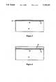
- FIG. 1 is a cross-sectional illustration of a semiconductor substrate showing the formation of field oxide layers using a silicon nitride mask.
- FIG. 2 is a cross-sectional illustration of a sacrificial oxide layer formed on a semiconductor substrate which has silicon-nitride spots due to the "Kooi effect”.
- FIG. 3 is a cross-sectional illustration of thermally grown silicon nitride layer formed on a semiconductor substrate.
- FIG. 4 is a cross-sectional illustration of an oxide layer deposited on top of the silicon nitride layer.
- FIG. 5 is a cross-sectional illustration of the composite dielectric layer of the present invention formed on a silicon substrate.
- FIG. 6 is a cross-sectional illustration of a lightly doped drain (LDD) MOS transistor using the composite dielectric layer of the present invention.
- LDD lightly doped drain
- the present invention discloses a novel composite dielectric layer for semiconductor devices.
- numerous specific details are set forth in order to provide a thorough understanding of the present invention.
- the present invention may be practiced without these specific details.
- well-known semiconductor concepts and fabrication techniques have not been set forth in detail in order to not unnecessarily obscure the present invention.
- the present invention is a novel composite dielectric layer for a semiconductor device.
- the composite dielectric is a high quality, highly reliable, ULSI manufacturable, dielectric layer.
- the composite dielectric layer is an oxynitride film formed by an Oxidation of Deposited Oxide on a Nitrided silicon surface (ODON).
- the composite film is formed by a thermal nitridation of a silicon wafer in pure ammonia (NH 3 ) or nitrous oxide (N 2 O), followed by a high temperature oxide (HTO) deposition, and a final anneal in oxygen ambient (reoxidation).
- the novel composite dielectric layer of the present invention exhibits excellent electrical characteristics such as very large charge-to-breakdown, considerable reduction in charge trapping, reduction of interface state generation and immunity to transconductance degradation.
- the composite dielectric layer of the present invention exhibits superior electrical and reliability characteristics at thicknesses below 200 ⁇ .
- the composite dielectric therefore, is ideal for future scaled semiconductor devices such as transistors and EEPROMS, which require thin, high quality dielectrics.
- the composite dielectric layer of the present invention is formed by a process which forms uniform and precise thickness layers. The process is therefore well suited to an ultra large scale integration (ULSI) manufacturing environment. Additionally, the novel process can be easily implemented into standard CMOS technology without altering other process sequences.
- ULSI ultra large scale integration
- novel composite dielectric layer of the present invention is described in reference to the formation of a thin gate insulating layer for a transistor, it is to be appreciated that the method of the present invention can be used to form a dielectric layer in any application where a thin, high quality dielectric is required, such as in a tunnel oxide for an EEPROM device.
- the fabrication of a NMOS field effect transistor begins with a starting material of a lightly doped (5 ⁇ 10 14 atoms/cm 2 ) p-type ⁇ 100> silicon wafer 10.
- the silicon wafer 10 is then defined with well-known isolation techniques into active regions 12 and field regions 13.
- isolation is accomplished by first growing a thin (200-600 ⁇ ) pad oxide layer 18 on the silicon wafer 10 for stress relief.
- a 1000-2000 ⁇ silicon-nitride layer 16 is deposited by CVD on the pad oxide 18 layer.
- a mask is then used to expose a resist film that was spun on after the nitride deposition. After exposure and development, the resist layer remains behind only over the regions 12 that will be the active device regions.
- the nitride 16 and pad oxide 18 are anisotropically etched away in the regions 17 not covered by resist.
- the active areas 12 are covered with a nitride/pad oxide layer 16/18 which acts as an isolation mask.
- Boron can be implanted next to form channel stops in the field regions 13.
- thermal oxidation occurs.
- the thermal oxidation step grows an approximately 4000-10,000 ⁇ thick field oxide layer 14 over field regions 13.
- the field oxide 14 grows only at those locations 17 where the pad oxide/nitride layer has been etched away.
- the remaining portions of nitride/pad oxide layer 16/18 are removed, leaving the active area 12 with exposed silicon.
- silicon-nitride spots or ribbons 21 are formed at the silicon/pad oxide interface. These spots 21 are caused by the well known and documented "Kooi effect".
- the "Kooi effect” refers to the fact that a thin layer of silicon nitride can form on the silicon surface from reaction of H 2 O and the masking nitride 16 during the field oxidation step to form NH 3 .
- the NH 3 then diffuses through the pad oxide 18 and reacts with the silicon substrate 10 to form silicon-nitride spots or ribbons 21 (these regions are sometimes called white ribbons).
- Silicon nitride impedes the growth rate of thermal oxides at locations 21 where it has formed.
- gate insulators which use a thermally grown oxide layer unlike the present invention, can have thin areas at these locations, resulting in a gate insulating layer which is nonuniform and exhibits poor reliability and performance characteristics.
- an approximately 350 ⁇ sacrificial oxide layer 22 is grown over the exposed active region 12 of substrate 10.
- the sacrificial oxide step prepares the silicon substrate for the formation of the gate dielectric.
- the sacrificial oxide layer 22 removes contaminants such as dry-etch induced damage and silicon-nitride spots or ribbons 21 formed by the "Kooi effect". Even the use of a sacrificial oxide layer, as in the present invention, does not remove all of the silicon nitride spots so that if a gate insulator with a thermally grown oxide layer is formed, it would still suffer to some degree from "white ribbon effects".
- the sacrificial oxide layer 22 is removed with a wet etchant, such as HF.
- a wet etchant such as HF.
- the substrate 10 is then rinsed and dried so that a high quality gate insulating layer can be formed over the active region 12 of substrate 10.
- the first layer of the composite dielectric layer is formed over the active region 12 of substrate 10.
- the first layer is a very thin silicon nitride (Si 3 N 4 ) film 23 grown to a thickness of less than 30 ⁇ .
- the silicon nitride layer is formed by direct thermal nitridation of the Si substrate 10 with an ambient of pure ammonia (NH 3 ) at a temperature in the range of 840°-855° C. and at a pressure of between 600-700 mTORR for a time between 1-3 hours. The process is carried out in a TMX-10K diffusion furnace or equivalent means.
- the thermal nitridation of silicon in the present invention forms a uniform concentration of nitrogen at the silicon interface. It is to be noted that because there is a small amount of native oxide present on the substrate 10 during nitridation, the thermal nitridation process forms an oxynitride layer at the silicon/silicon-nitride interface 20 with a slightly more than 1:1 concentration of nitrogen to oxygen.
- the composite dielectric of the present invention does not suffer from "white ribbon "effects" as do gate dielectrics comprising thermally grown oxides.
- thermal nitridation of silicon has self limiting growth kinetics, its thickness and resultant nitrogen concentration can be easily controlled by well known process parameters.
- the ability to form uniform and precise thickness layers is essential in the formation of thin gate dielectric layers for ULSI circuits. It is to be appreciated that a gate insulator is an active component of a transistor and its resulting thickness directly effects device performance and reliability.
- a high temperature oxide (HTO) film 24 with a thickness range of 65-165 ⁇ is deposited on top of the silicon nitride film 23.
- the high temperature SiO 2 film is formed by low pressure chemical vapor deposition (LPCVD) at a temperature in the range of 800°-850° C. and at a pressure between 300-350 mTORR for about 30 minutes.
- the high temperature LPCVD film is deposited from nitrous oxide (N 2 O) and dichlorosilane (SiH 2 CL 2 ) sources.
- a TMX-10K furnace can be used for the deposition.
- the high temperature LPCVD process produces a high quality SiO 2 layer which has a controllable thickness and excellent uniformity across a wafer. As mentioned before the ability to form uniform, precise thickness layers is essential when forming such thin gate dielectric layers.
- the HTO deposition process can be completed with an optional anneal at 920° C. in an N 2 ambient for 15-40 minutes. The optional anneal compacts or densifies the HTO layer and improves its dielectric properties.
- the formation of the novel composite dielectric layer is completed with an oxygen anneal or reoxidation step.
- the oxygen anneal step is a dry oxidation with trichloroethane (TCA).
- TCA trichloroethane
- the substrate 10 is placed in a TMX-10K furnace at a temperature of about 800°-920° C. for 20-90 minutes in the presence of approximately 9% TCA and O 2 at atmospheric pressure.
- the oxygen anneal or reoxidation process reduces and optimizes the residual concentration of nitrogen and hydrogen in the insulator bulk and at the silicon/insulator interface.
- the dry oxidation step decreases electron trapping and interface state generation in the dielectric layer.
- the formation of the composite dielectric layer of the present invention is now complete.
- the individual atoms of the dielectric film diffuse into a structure which is responsible for its superior electrical characteristics.
- the structure of the resulting dielectric layer has a low, uniform (about 1%) nitrogen concentration at the silicon/insulator interface optimized to prevent interface state generation.
- the Si--N bonds at the interface replace trained Si--O and Si--H bonds which cause interface state generation which leads to performance degradation and eventually to breakdown.
- the resulting structure of the composite dielectric exhibits a nitrogen concentration in the bulk of the insulator which has been optimized to prevent bulk trapping.
- the final structure of the composite dielectric layer 25 is responsible for its excellent electrical characteristics at thicknesses less than a 200 ⁇ .
- an important aspect of the present invention is the ability to independently control the nitrogen concentration at the silicon/insulator interface 26 and the nitrogen concentration in the bulk of the insulator. This is due to the fact that the nitrogen concentration at the silicon/insulator interface 26 is determined by the amount of nitrogen generated during the thermal nitridation of the silicon substrate, minus the amount of nitrogen driven out by the subsequent reoxidation process; and due to the fact that the nitrogen concentration in the bulk of the insulator is determined by the amount of nitrogen driven out of the silicon/insulator interface and into the bulk of the insulator by the reoxidation process. Thus, one is able to provide the desired amount of nitrogen required for both the silicon/insulator interface and the bulk with the thermal nitridation step.
- the nitrogen concentration at the interface is set by first growing an uniform silicon nitride layer at the silicon interface and then diffusing excess amounts of nitrogen out of the interface and into the insulator bulk and ambient, the uniformity of the nitrogen concentration at the interface is excellent in the present invention.
- the "double diffusion" process of first diffusing nitrogen in through the oxide layer (nitridation) and then diffusing out excess nitrogen (reoxitation) may cause a nonuniform nitrogen concentration to form at the silicon interface.
- the structure of composite dielectric layer exhibits a lower defect density than do prior art NO or RNO layers.
- the low defect density is due to the composite nature of the insulator of the present invention. Local defects can arise in the formation of the silicon nitride layer and defects can also arise in the formation of the HTO layer. However, it is highly unlikely that the defects from the two independently formed layers will line up and create a defect which extends from the surface of the insulator to the silicon interface. Thus, a low defect density is expected and experienced in the composite dielectric layer of the present invention.
- the method of fabrication of the present invention provides a highly uniform, precise thickness dielectric layer. This is because the thermal nitridation process forms a silicon nitride layer which has fixed growth kinetics and which does not suffer the "Kooi" effect, and because the HTO process yields an oxide layer which is extremely uniform and whose thickness can be easily controlled. Thus, a composite dielectric layer with an excellent uniformity and a precisely controlled thickness can be formed across an entire wafer surface. It is important to recall that gate insulators are active components of semiconductor transistors whose thicknesses greatly affect device performance. Thus a manufacturable gate insulator process is extremely important for future high-density ICs where literally tens of millions of gate insulators will be formed.
- the remaining features of the NMOS transistor are fabricated in accordance with well known techniques. Namely, first, if desired, a threshold voltage implant is made. Next, a polysilicon layer is formed over the composite gate dielectric layer, and then doped and patterned into a gate electrode 27. A low conductivity source/drain implant is then made of n type impurities into the silicon substrate 10 in alignment with the outside edges of the polysilicon gate 26 to form a lightly doped drain 28. Next oxide spacers 29 are formed and a second higher conductivity source/drain implant of n type impurities is made into the silicon substrate 10 in alignment with the oxide spacers to form source/drain regions 30 of the device. In this way a short channeled transistor 31 has been fabricated. The transistor features a less than 100 ⁇ thick high quality, highly reliable, composite gate dielectric 32.
- the composite gate insulator 32 of the present invention exhibits outstanding electrical and reliability characteristics.
- the composite gate dielectric layer 32 exhibits reduced interface state generation and bulk trapping.
- the composite dielectric layer 32 also exhibits a good "charge to breakdown” characteristic.
- the composite dielectric layer 32 has good endurance to charge injection and breakdown fields.
- the composite dielectric layer has a great potential for use in non-volatile memories such as E 2 PROMS and FLASH EPROMS due to its reduced trapping and increased "charge to breakdown" in tunneling stress.
- the thin composite dielectric layer exhibits outstanding electrical and reliability characteristics and can be realized with a ULSI manufacturable process (without the use of RTP).
Landscapes
- Engineering & Computer Science (AREA)
- Physics & Mathematics (AREA)
- Condensed Matter Physics & Semiconductors (AREA)
- General Physics & Mathematics (AREA)
- Manufacturing & Machinery (AREA)
- Computer Hardware Design (AREA)
- Microelectronics & Electronic Packaging (AREA)
- Power Engineering (AREA)
- Chemical & Material Sciences (AREA)
- Chemical Kinetics & Catalysis (AREA)
- Formation Of Insulating Films (AREA)
Abstract
A high-quality, highly reliable, composite dielectric layer for a semiconductor device. The composite dielectric layer is formed by nitriding a silicon surface, forming an oxide layer on the nitrided silicon surface, and then annealing the nitrided-silicon surface and the oxide in an oxygen ambient.
Description
1. Field of the Invention
The present invention relates to the field of semiconductor devices, and more specifically to a gate dielectric layer for semiconductor device and a method of making the same.
2. Description of Related Art
One of the most important features required for the production of future small scaled semiconductor devices is a thin highly reliable insulating layer. The drive for ultra large scale integration (ULSI) implies shrinking of transistor dimensions and consequentially, a need for an ultrathin (<200 Å) highly reliable gate insulator. Additionally, highly reliable dielectrics are required for scaled floating gate memories, because their tunnel oxide film suffers from high field (>8 MV/cm) stress during device operation resulting in the limitation of data retention times as well as read/write cycles.
Scaled semiconductor devices will require thin dielectric layers which exhibit excellent electrical and reliability characteristics. For example, future technologies will require gate dielectric layers with reduced interface state generation and bulk trapping, and improved endurance to charge injection and high breakdown fields. Floating gate memories in particular will require dielectric layers which exhibit reduced trapping and increased "charge to breakdown" in tunneling stress. Additionally, due to high integration and thin layer requirements, future technologies will require a dielectric layer with an extremely uniform and manufacturable process.
Present gate insulating layers fall short of the requirements necessary for future small scale devices. Most conventional gate insulating layers are pure SiO2 oxide films formed by thermal oxidation. Others employ a combination of a high temperature deposited SiO2 layer on a thermally grown oxide layer. Pure SiO2 layers are unsuitable for future devices because their integrity is inadequate when formed to thicknesses below 150 Å. That is, they suffer from their inherent physical and electrical limitations. Still further, SiO2 layers suffer from their inability to be manufactured uniformly and defect-free when formed thin. Additionally, subsequent ULSI processing steps continue to degrade the already fragile integrity of thin SiO2 layers. In addition pure SiO2 layers tend to degrade, when exposed to charge injection, by interface generation and charge trapping. As such, pure SiO2 layers are simply inadequate as thin films for future scaled technologies.
Nitrided oxides (NO) have recently been proposed as a substitute to pure SiO2 layers in future semiconductor devices. Nitrided oxides exhibit a number of characteristics such as: improved electrical characteristics under stress, insensitivity to radiation, and a barrier to various dopants, which make them attractive as gate dielectrics for a number of applications. Nitrided oxides are generally formed by first thermally growing an SiO2 layer and then later exposing the oxide layer to a pure ammonia (NH3) high temperature anneal in order to nitride the oxide. Unfortunately, nitrided oxides (NO) formed by annealing in pure ammonia (NH3) suffer from increased electron trapping due to the large amount of ammonia, and hence hydrogen causing traps which are introduced into the dielectric during nitridation.
To combat these problems reoxidation of nitrided oxides (RNO) has been proposed. Reoxidation of nitrided oxides show both a decrease in electron trapping and interface state generation. These improvements are attributed to the incorporation of a relatively small amount of nitrogen at the silicon/dielectric interface without introducing a large amount of hydrogen. The reoxidation process essentially drives in oxygen atoms to drive out excess nitrogen atoms at the insulator/silicon interface which were formed during the nitridation process.
A problem with reoxidized nitrided oxides (RNO) is that because of the way they are formed, they lack a uniform nitrogen concentration at the silicon/insulator interface and the ability to independently control the nitrogen concentration at the silicon/insulator interface and the nitrogen concentration in the bulk of the insulator. Since the nitrogen concentration of the insulator is set by first diffusing a large nitrogen concentration through the oxide layer into the interface (nitridation) and then driving out with oxygen (reoxidation) excess nitrogen, the nitrogen concentration uniformity suffers. Additionally, because the nitrogen concentration in the bulk of the insulator and the nitrogen concentration at the interface are both determined by the same nitridation and subsequent reoxidation process, their nitrogen concentrations can not be independently controlled to optimize electrical characteristics.
Another problem with both NO and RNO films is that they use thermally grown oxides. Thermally grown oxide layers are susceptible to the "Kooi" effect which causes thickness variation in the grown layer. Thickness variations in the oxide layer translates into performance, reliability, and manufacturing problems. Additionaly, many present NO and RNO processes utilize Rapid Thermal Nitridation (RTN) which is a short time, high temperature nitridation process. Such a rapid thermal process can cause wafer warpage, an undesired redistribution of dopants, and the creation of slip dislocations in the crystal lattice.
Thus, what is needed is a thin dielectric layer which can meet the electrical and reliability requirements of future scaled semiconductor devices, and which can be formed easily and uniformly in a ULSI environment.
The present invention is a novel composite dielectric layer for a semiconductor device. The composite dielectric layer is formed by first growing a sacrificial oxide layer on a semiconductor substrate, and then stripping the oxide layer with HF, followed by a standard rinse and dry. The sacrificial oxide layer helps to eliminate contaminants found on the surface of the silicon substrate. Next, a silicon nitride film is grown. The silicon nitride film is grown by thermal nitridation of the silicon substrate in pure ammonia (NH3). Next a high temperature oxide (HTO) is deposited on the silicon nitride layer by a LPCVD process from nitrous oxide and dichlorosilane sources. An optional high temperature anneal in N2 can then be carried out in order to densify and improve the characteristics of the high temperature oxide. Finally, to complete the fabrication of the composite dielectric layer, the silicon substrate and the formed composite layer are subjected to a reoxidation by a dry oxidation process.
A goal of the present invention is to provide a thin, high quality, highly reliable dielectric layer which can be used in future small-scale semiconductor devices.
Another goal of the present invention is to provide a composite gate dielectric which exhibits outstanding electrical and reliability characteristics when formed to thicknesses in the range of 50-200 Å.
Still another goal of the present invention is to form such a dielectric layer with a process which affords precise thickness control and uniformity across a wafer so that it is ULSI manufacturable.
Still yet another goal of the present invention is to provide an improved nitride-oxide film which is formed with a process which generates a uniform nitrogen concentration at the silicon/insulator interface and which provides freedom to independently optimize the nitrogen concentration in the bulk of the insulator and the nitrogen concentration at the silicon/insulator interface.
Still yet another goal of the present invention is to form a dielectric layer with processing temperatures below 950° C. without the need to use RTP.
FIG. 1 is a cross-sectional illustration of a semiconductor substrate showing the formation of field oxide layers using a silicon nitride mask.
FIG. 2 is a cross-sectional illustration of a sacrificial oxide layer formed on a semiconductor substrate which has silicon-nitride spots due to the "Kooi effect".
FIG. 3 is a cross-sectional illustration of thermally grown silicon nitride layer formed on a semiconductor substrate.
FIG. 4 is a cross-sectional illustration of an oxide layer deposited on top of the silicon nitride layer.
FIG. 5 is a cross-sectional illustration of the composite dielectric layer of the present invention formed on a silicon substrate.
FIG. 6 is a cross-sectional illustration of a lightly doped drain (LDD) MOS transistor using the composite dielectric layer of the present invention.
The present invention discloses a novel composite dielectric layer for semiconductor devices. In the following description, numerous specific details are set forth in order to provide a thorough understanding of the present invention. However, it will be obvious to one skilled in the art that the present invention may be practiced without these specific details. In other instances, well-known semiconductor concepts and fabrication techniques have not been set forth in detail in order to not unnecessarily obscure the present invention.
The present invention is a novel composite dielectric layer for a semiconductor device. The composite dielectric is a high quality, highly reliable, ULSI manufacturable, dielectric layer. The composite dielectric layer is an oxynitride film formed by an Oxidation of Deposited Oxide on a Nitrided silicon surface (ODON). The composite film is formed by a thermal nitridation of a silicon wafer in pure ammonia (NH3) or nitrous oxide (N2 O), followed by a high temperature oxide (HTO) deposition, and a final anneal in oxygen ambient (reoxidation). The novel composite dielectric layer of the present invention exhibits excellent electrical characteristics such as very large charge-to-breakdown, considerable reduction in charge trapping, reduction of interface state generation and immunity to transconductance degradation. The composite dielectric layer of the present invention exhibits superior electrical and reliability characteristics at thicknesses below 200 Å. The composite dielectric, therefore, is ideal for future scaled semiconductor devices such as transistors and EEPROMS, which require thin, high quality dielectrics. Additionally, the composite dielectric layer of the present invention is formed by a process which forms uniform and precise thickness layers. The process is therefore well suited to an ultra large scale integration (ULSI) manufacturing environment. Additionally, the novel process can be easily implemented into standard CMOS technology without altering other process sequences.
Although the formation of the novel composite dielectric layer of the present invention is described in reference to the formation of a thin gate insulating layer for a transistor, it is to be appreciated that the method of the present invention can be used to form a dielectric layer in any application where a thin, high quality dielectric is required, such as in a tunnel oxide for an EEPROM device.
In reference to FIG. 1, the fabrication of a NMOS field effect transistor begins with a starting material of a lightly doped (5×10¹⁴ atoms/cm2) p-type <100> silicon wafer 10. The silicon wafer 10 is then defined with well-known isolation techniques into active regions 12 and field regions 13. In one method, isolation is accomplished by first growing a thin (200-600 Å) pad oxide layer 18 on the silicon wafer 10 for stress relief. Next a 1000-2000 Å silicon-nitride layer 16 is deposited by CVD on the pad oxide 18 layer. A mask is then used to expose a resist film that was spun on after the nitride deposition. After exposure and development, the resist layer remains behind only over the regions 12 that will be the active device regions. Next the nitride 16 and pad oxide 18 are anisotropically etched away in the regions 17 not covered by resist. Thus after the removal of the resist, the active areas 12 are covered with a nitride/pad oxide layer 16/18 which acts as an isolation mask. Boron can be implanted next to form channel stops in the field regions 13. Next, thermal oxidation occurs. The thermal oxidation step grows an approximately 4000-10,000 Å thick field oxide layer 14 over field regions 13. The field oxide 14 grows only at those locations 17 where the pad oxide/nitride layer has been etched away. After the field oxide has been grown, the remaining portions of nitride/pad oxide layer 16/18 are removed, leaving the active area 12 with exposed silicon.
Unfortunately, during isolation formation undesired silicon-nitride spots or ribbons 21 are formed at the silicon/pad oxide interface. These spots 21 are caused by the well known and documented "Kooi effect". The "Kooi effect" refers to the fact that a thin layer of silicon nitride can form on the silicon surface from reaction of H2 O and the masking nitride 16 during the field oxidation step to form NH3. The NH3 then diffuses through the pad oxide 18 and reacts with the silicon substrate 10 to form silicon-nitride spots or ribbons 21 (these regions are sometimes called white ribbons). Silicon nitride impedes the growth rate of thermal oxides at locations 21 where it has formed. Thus gate insulators which use a thermally grown oxide layer, unlike the present invention, can have thin areas at these locations, resulting in a gate insulating layer which is nonuniform and exhibits poor reliability and performance characteristics.
After isolation, as shown in FIG. 2, an approximately 350 Å sacrificial oxide layer 22 is grown over the exposed active region 12 of substrate 10. The sacrificial oxide step prepares the silicon substrate for the formation of the gate dielectric. The sacrificial oxide layer 22 removes contaminants such as dry-etch induced damage and silicon-nitride spots or ribbons 21 formed by the "Kooi effect". Even the use of a sacrificial oxide layer, as in the present invention, does not remove all of the silicon nitride spots so that if a gate insulator with a thermally grown oxide layer is formed, it would still suffer to some degree from "white ribbon effects". Just prior to gate insulator formation the sacrificial oxide layer 22 is removed with a wet etchant, such as HF. The substrate 10 is then rinsed and dried so that a high quality gate insulating layer can be formed over the active region 12 of substrate 10.
Referring now to FIG. 3, after sufficient cleaning of the silicon substrate, the first layer of the composite dielectric layer is formed over the active region 12 of substrate 10. The first layer is a very thin silicon nitride (Si3 N4) film 23 grown to a thickness of less than 30 Å. In the preferred embodiment of the present invention, the silicon nitride layer is formed by direct thermal nitridation of the Si substrate 10 with an ambient of pure ammonia (NH3) at a temperature in the range of 840°-855° C. and at a pressure of between 600-700 mTORR for a time between 1-3 hours. The process is carried out in a TMX-10K diffusion furnace or equivalent means. The thermal nitridation of silicon in the present invention, unlike the prior art technique, forms a uniform concentration of nitrogen at the silicon interface. It is to be noted that because there is a small amount of native oxide present on the substrate 10 during nitridation, the thermal nitridation process forms an oxynitride layer at the silicon/silicon-nitride interface 20 with a slightly more than 1:1 concentration of nitrogen to oxygen.
It is to be appreciated that because the first layer is a thermally grown Si3 N4 layer and not a thermally grown SiO2 oxide layer, as in the prior art, the composite dielectric of the present invention does not suffer from "white ribbon "effects" as do gate dielectrics comprising thermally grown oxides. Additionally because thermal nitridation of silicon has self limiting growth kinetics, its thickness and resultant nitrogen concentration can be easily controlled by well known process parameters. The ability to form uniform and precise thickness layers is essential in the formation of thin gate dielectric layers for ULSI circuits. It is to be appreciated that a gate insulator is an active component of a transistor and its resulting thickness directly effects device performance and reliability.
Next, in reference to FIG. 4 a high temperature oxide (HTO) film 24 with a thickness range of 65-165 Å is deposited on top of the silicon nitride film 23. In the preferred embodiment of the present invention, the high temperature SiO2 film is formed by low pressure chemical vapor deposition (LPCVD) at a temperature in the range of 800°-850° C. and at a pressure between 300-350 mTORR for about 30 minutes. The high temperature LPCVD film is deposited from nitrous oxide (N2 O) and dichlorosilane (SiH2 CL2) sources. A TMX-10K furnace can be used for the deposition. The high temperature LPCVD process produces a high quality SiO2 layer which has a controllable thickness and excellent uniformity across a wafer. As mentioned before the ability to form uniform, precise thickness layers is essential when forming such thin gate dielectric layers. The HTO deposition process can be completed with an optional anneal at 920° C. in an N2 ambient for 15-40 minutes. The optional anneal compacts or densifies the HTO layer and improves its dielectric properties.
In reference to FIG. 5 the formation of the novel composite dielectric layer is completed with an oxygen anneal or reoxidation step. In the preferred embodiment of the present invention, the oxygen anneal step is a dry oxidation with trichloroethane (TCA). The substrate 10 is placed in a TMX-10K furnace at a temperature of about 800°-920° C. for 20-90 minutes in the presence of approximately 9% TCA and O2 at atmospheric pressure. The oxygen anneal or reoxidation process reduces and optimizes the residual concentration of nitrogen and hydrogen in the insulator bulk and at the silicon/insulator interface. The dry oxidation step decreases electron trapping and interface state generation in the dielectric layer. The formation of the composite dielectric layer of the present invention is now complete.
It is to be appreciated that during the formation of the dielectric layer of the present invention, the individual atoms of the dielectric film diffuse into a structure which is responsible for its superior electrical characteristics. The structure of the resulting dielectric layer has a low, uniform (about 1%) nitrogen concentration at the silicon/insulator interface optimized to prevent interface state generation. The Si--N bonds at the interface replace trained Si--O and Si--H bonds which cause interface state generation which leads to performance degradation and eventually to breakdown. Additionally, the resulting structure of the composite dielectric exhibits a nitrogen concentration in the bulk of the insulator which has been optimized to prevent bulk trapping. The final structure of the composite dielectric layer 25 is responsible for its excellent electrical characteristics at thicknesses less than a 200 Å.
It is to be appreciated that an important aspect of the present invention is the ability to independently control the nitrogen concentration at the silicon/insulator interface 26 and the nitrogen concentration in the bulk of the insulator. This is due to the fact that the nitrogen concentration at the silicon/insulator interface 26 is determined by the amount of nitrogen generated during the thermal nitridation of the silicon substrate, minus the amount of nitrogen driven out by the subsequent reoxidation process; and due to the fact that the nitrogen concentration in the bulk of the insulator is determined by the amount of nitrogen driven out of the silicon/insulator interface and into the bulk of the insulator by the reoxidation process. Thus, one is able to provide the desired amount of nitrogen required for both the silicon/insulator interface and the bulk with the thermal nitridation step. (Actually excess silicon-nitride is grown because some nitrogen escapes to the ambient during reoxidation.) One is then able to use the reoxidation step to set both the nitrogen interface concentration and the bulk nitrogen concentration with the reoxidation step. (i.e., the excess nitrogen at the interface is diffused out of the interface and into the bulk thereby setting the bulk concentration.) In this way the nitrogen concentration in the bulk of the insulator can be optimized to prevent trapping and the nitrogen concentration at the silicon/insulator interface can be optimized to prevent interface state generation. Such optimal control of nitrogen concentrations at different locations in the insulator was unavailable with the prior art RNO technique.
Additionally, because the nitrogen concentration at the interface is set by first growing an uniform silicon nitride layer at the silicon interface and then diffusing excess amounts of nitrogen out of the interface and into the insulator bulk and ambient, the uniformity of the nitrogen concentration at the interface is excellent in the present invention. Wherein in the prior art the "double diffusion" process of first diffusing nitrogen in through the oxide layer (nitridation) and then diffusing out excess nitrogen (reoxitation) may cause a nonuniform nitrogen concentration to form at the silicon interface.
Additionally, the structure of composite dielectric layer exhibits a lower defect density than do prior art NO or RNO layers. The low defect density is due to the composite nature of the insulator of the present invention. Local defects can arise in the formation of the silicon nitride layer and defects can also arise in the formation of the HTO layer. However, it is highly unlikely that the defects from the two independently formed layers will line up and create a defect which extends from the surface of the insulator to the silicon interface. Thus, a low defect density is expected and experienced in the composite dielectric layer of the present invention.
The method of fabrication of the present invention provides a highly uniform, precise thickness dielectric layer. This is because the thermal nitridation process forms a silicon nitride layer which has fixed growth kinetics and which does not suffer the "Kooi" effect, and because the HTO process yields an oxide layer which is extremely uniform and whose thickness can be easily controlled. Thus, a composite dielectric layer with an excellent uniformity and a precisely controlled thickness can be formed across an entire wafer surface. It is important to recall that gate insulators are active components of semiconductor transistors whose thicknesses greatly affect device performance. Thus a manufacturable gate insulator process is extremely important for future high-density ICs where literally tens of millions of gate insulators will be formed.
In reference to FIG. 6 the remaining features of the NMOS transistor are fabricated in accordance with well known techniques. Namely, first, if desired, a threshold voltage implant is made. Next, a polysilicon layer is formed over the composite gate dielectric layer, and then doped and patterned into a gate electrode 27. A low conductivity source/drain implant is then made of n type impurities into the silicon substrate 10 in alignment with the outside edges of the polysilicon gate 26 to form a lightly doped drain 28. Next oxide spacers 29 are formed and a second higher conductivity source/drain implant of n type impurities is made into the silicon substrate 10 in alignment with the oxide spacers to form source/drain regions 30 of the device. In this way a short channeled transistor 31 has been fabricated. The transistor features a less than 100 Å thick high quality, highly reliable, composite gate dielectric 32.
The composite gate insulator 32 of the present invention exhibits outstanding electrical and reliability characteristics. The composite gate dielectric layer 32 exhibits reduced interface state generation and bulk trapping. The composite dielectric layer 32 also exhibits a good "charge to breakdown" characteristic. Additionally, the composite dielectric layer 32 has good endurance to charge injection and breakdown fields. In addition to its use in standard MOS technology the composite dielectric layer has a great potential for use in non-volatile memories such as E2 PROMS and FLASH EPROMS due to its reduced trapping and increased "charge to breakdown" in tunneling stress.
Thus a novel composite dielectric layer for future small-scale semiconductor devices has been described. The thin composite dielectric layer exhibits outstanding electrical and reliability characteristics and can be realized with a ULSI manufacturable process (without the use of RTP).
Claims (14)
1. A method of forming a composite dielectric layer for a semiconductor device comprising the steps of:
nitriding a silicon surface;
forming an oxide layer on said nitrided silicon surface;
oxidizing said oxide layer and said nitrided silicon surface to from said composite dielectric layer; and
forming said device on said composite dielectric layer.
2. A method of forming a composite dielectric layer for a semiconductor device on a silicon substrate comprising the steps of:
forming a silicon nitride layer on said silicon substrate;
forming an oxide layer on said silicon nitride layer;
oxidizing said layers to form said composite dielectric layer; and
forming said device on said composite dielectric layer.
3. The method of claim 2 further comprising a step of annealing said oxide layer in an N2 ambient after formation of said oxide layer.
4. The method of claim 2 further comprising a step of growing a sacrificial oxide layer on said substrate and stripping said sacrificial oxide layer prior to said step of forming silicon nitride layer.
5. The method of claim 2 wherein said step of forming said silicon nitride layer is a thermal nitridation of said silicon substrate.
6. The method of claim 5 wherein said thermal nitridation of said silicon substrate is accomplished by exposing said silicon substrate to a pure ammonia or nitrous oxide ambient at a reduced pressure.
7. The method of claim 2 wherein said step of forming said oxide layer is a CVD deposition of SiO2.
8. The method of claim 7 wherein said CVD deposition of SiO2 is a high temperature low pressure CVD deposition from nitrous oxide and dichlorosilane sources.
9. The method of claim 2 wherein said oxidizing step is a dry oxidation with TCA.
10. A method of forming a high quality, highly reliable ULSI manufacturable composite dielectric layer for a semiconductor device formed on a silicon substrate comprising the steps of:
thermally growing a silicon nitride layer on said silicon substrate by exposing said silicon substrate to pure ammonia at a reduced pressure;
depositing a high temperature oxide layer on said silicon nitride layer by CVD;
oxidizing said thermally grown silicon nitride layer and said deposited high temperature oxide layer in an ambient comprising O2 and TCA to form said composite dielectric layer; and
forming said device on said composite dielectric layer.
11. The method of claim 10 wherein said thermally grown silicon nitride layer is grown to less than 30 Å thick.
12. The method of claim 10 wherein said CVD deposited oxide layer is between 65-165 Å thick.
13. The method of claim 10 further comprising a step of annealing said substrate in an N2 ambient at a temperature of approximately 920° C.
14. The method of claim 10 wherein said step of depositing said high temperature oxide layer is a low pressure CVD deposition.
Priority Applications (1)
| Application Number | Priority Date | Filing Date | Title |
|---|---|---|---|
| US07/931,596 US5258333A (en) | 1992-08-18 | 1992-08-18 | Composite dielectric for a semiconductor device and method of fabrication |
Applications Claiming Priority (1)
| Application Number | Priority Date | Filing Date | Title |
|---|---|---|---|
| US07/931,596 US5258333A (en) | 1992-08-18 | 1992-08-18 | Composite dielectric for a semiconductor device and method of fabrication |
Publications (1)
| Publication Number | Publication Date |
|---|---|
| US5258333A true US5258333A (en) | 1993-11-02 |
Family
ID=25461037
Family Applications (1)
| Application Number | Title | Priority Date | Filing Date |
|---|---|---|---|
| US07/931,596 Expired - Lifetime US5258333A (en) | 1992-08-18 | 1992-08-18 | Composite dielectric for a semiconductor device and method of fabrication |
Country Status (1)
| Country | Link |
|---|---|
| US (1) | US5258333A (en) |
Cited By (62)
| Publication number | Priority date | Publication date | Assignee | Title |
|---|---|---|---|---|
| US5382533A (en) * | 1993-06-18 | 1995-01-17 | Micron Semiconductor, Inc. | Method of manufacturing small geometry MOS field-effect transistors having improved barrier layer to hot electron injection |
| US5397720A (en) * | 1994-01-07 | 1995-03-14 | The Regents Of The University Of Texas System | Method of making MOS transistor having improved oxynitride dielectric |
| US5407870A (en) * | 1993-06-07 | 1995-04-18 | Motorola Inc. | Process for fabricating a semiconductor device having a high reliability dielectric material |
| US5478765A (en) * | 1994-05-04 | 1995-12-26 | Regents Of The University Of Texas System | Method of making an ultra thin dielectric for electronic devices |
| US5489542A (en) * | 1990-11-28 | 1996-02-06 | Kabushiki Kaisha Toshiba | Method for fabricating semiconductor device in which threshold voltage shift and charge-pumping current are improved |
| US5543343A (en) * | 1993-12-22 | 1996-08-06 | Sgs-Thomson Microelectronics, Inc. | Method fabricating an integrated circuit |
| US5571734A (en) * | 1994-10-03 | 1996-11-05 | Motorola, Inc. | Method for forming a fluorinated nitrogen containing dielectric |
| EP0685883A3 (en) * | 1994-05-31 | 1997-10-08 | Sgs Thomson Microelectronics | Method of forming an improved dielectric in an integrated circuit. |
| US5712177A (en) * | 1994-08-01 | 1998-01-27 | Motorola, Inc. | Method for forming a reverse dielectric stack |
| US5712208A (en) * | 1994-06-09 | 1998-01-27 | Motorola, Inc. | Methods of formation of semiconductor composite gate dielectric having multiple incorporated atomic dopants |
| EP0825640A2 (en) * | 1996-07-29 | 1998-02-25 | Texas Instruments Incorporated | FET gate insulation and process for manufacturing |
| US5726087A (en) * | 1992-04-30 | 1998-03-10 | Motorola, Inc. | Method of formation of semiconductor gate dielectric |
| US5811865A (en) * | 1993-12-22 | 1998-09-22 | Stmicroelectronics, Inc. | Dielectric in an integrated circuit |
| US5834360A (en) * | 1996-07-31 | 1998-11-10 | Stmicroelectronics, Inc. | Method of forming an improved planar isolation structure in an integrated circuit |
| GB2325344A (en) * | 1997-05-14 | 1998-11-18 | Nec Corp | method of fabricating a gate insulator |
| US5866474A (en) * | 1997-07-17 | 1999-02-02 | United Microelectronics Corp. | Method for manufacturing gate oxide layers |
| US5888855A (en) * | 1994-12-14 | 1999-03-30 | Kabushiki Kaisha Toshiba | Method of manufacturing active matrix display |
| US5904523A (en) * | 1996-10-03 | 1999-05-18 | Lucent Technologies Inc. | Process for device fabrication in which a layer of oxynitride is formed at low temperatures |
| US5972800A (en) * | 1995-05-10 | 1999-10-26 | Nec Corporation | Method for fabricating a semiconductor device with multi-level structured insulator |
| US5972776A (en) * | 1995-12-22 | 1999-10-26 | Stmicroelectronics, Inc. | Method of forming a planar isolation structure in an integrated circuit |
| US6033998A (en) * | 1998-03-09 | 2000-03-07 | Lsi Logic Corporation | Method of forming variable thickness gate dielectrics |
| US6054396A (en) * | 1996-05-09 | 2000-04-25 | Micron Technology, Inc. | Semiconductor processing method of reducing thickness depletion of a silicide layer at a junction of different underlying layers |
| US6060369A (en) * | 1997-12-23 | 2000-05-09 | Advanced Micro Devices, Inc. | Nitrogen bearing sacrificial oxide with subsequent high nitrogen dopant profile for high performance MOSFET |
| US6087229A (en) * | 1998-03-09 | 2000-07-11 | Lsi Logic Corporation | Composite semiconductor gate dielectrics |
| US6104064A (en) * | 1996-10-01 | 2000-08-15 | Advanced Micro Devices, Inc. | Asymmetrical transistor structure |
| US6103555A (en) * | 1996-06-10 | 2000-08-15 | Integrated Device Technology, Inc. | Method of improving the reliability of low-voltage programmable antifuse |
| US6150286A (en) * | 2000-01-03 | 2000-11-21 | Advanced Micro Devices, Inc. | Method of making an ultra thin silicon nitride film |
| US6162687A (en) * | 1998-08-19 | 2000-12-19 | Advanced Micro Devices, Inc. | Method of manufacturing semiconductor device having oxide-nitride gate insulating layer |
| US6190973B1 (en) | 1998-12-18 | 2001-02-20 | Zilog Inc. | Method of fabricating a high quality thin oxide |
| US6215163B1 (en) * | 1997-03-10 | 2001-04-10 | Fujitsu Limited | Semiconductor device and method of manufacturing the same where the nitrogen concentration in an oxynitride insulating layer is varied |
| US6268285B1 (en) * | 1999-01-04 | 2001-07-31 | Advanced Micro Devices, Inc. | Method of removing plasma etch damage to pre-silicidized surfaces by wet silicon etch |
| US6271153B1 (en) * | 1998-07-22 | 2001-08-07 | Micron Technology, Inc. | Semiconductor processing method and trench isolation method |
| US6271120B1 (en) * | 1995-03-10 | 2001-08-07 | Advanced Micro Devices, Inc. | Method of enhanced silicide layer for advanced metal diffusion barrier layer application |
| US6274442B1 (en) * | 1998-07-15 | 2001-08-14 | Advanced Micro Devices, Inc. | Transistor having a nitrogen incorporated epitaxially grown gate dielectric and method of making same |
| US6380056B1 (en) * | 1998-10-23 | 2002-04-30 | Taiwan Semiconductor Manufacturing Company | Lightly nitridation surface for preparing thin-gate oxides |
| US6469329B1 (en) * | 1997-07-04 | 2002-10-22 | Nec Corporation | Solid state image sensing device and method of producing the same |
| US6482752B1 (en) * | 1993-10-26 | 2002-11-19 | Semiconductor Energy Laboratory Co., Ltd. | Substrate processing apparatus and method and a manufacturing method of a thin film semiconductor device |
| US6483157B1 (en) * | 1997-06-20 | 2002-11-19 | Advanced Micro Devices, Inc. | Asymmetrical transistor having a barrier-incorporated gate oxide and a graded implant only in the drain-side junction area |
| US6492217B1 (en) * | 1998-06-30 | 2002-12-10 | Intel Corporation | Complementary metal gates and a process for implementation |
| US6521518B1 (en) * | 2001-09-04 | 2003-02-18 | Macronix International Co., Ltd. | Method of eliminating weakness caused by high density plasma dielectric layer |
| US20030040171A1 (en) * | 2001-08-22 | 2003-02-27 | Weimer Ronald A. | Method of composite gate formation |
| US6531364B1 (en) * | 1998-08-05 | 2003-03-11 | Advanced Micro Devices, Inc. | Advanced fabrication technique to form ultra thin gate dielectric using a sacrificial polysilicon seed layer |
| US6548366B2 (en) * | 2001-06-20 | 2003-04-15 | Texas Instruments Incorporated | Method of two-step annealing of ultra-thin silicon dioxide layers for uniform nitrogen profile |
| US6566282B2 (en) * | 2001-06-21 | 2003-05-20 | United Microelectronics Corp. | Method of forming a silicon oxide layer |
| DE10133537C2 (en) * | 2001-07-11 | 2003-07-17 | Infineon Technologies Ag | Process for producing a nitrided oxide layer on a silicon semiconductor substrate |
| US20030181012A1 (en) * | 2002-03-20 | 2003-09-25 | Taiwan Semiconductor Manufacturing Co., Ltd. | Method of making an ultrathin silicon dioxide gate with improved dielectric properties using NH3 nitridation and post-deposition rapid thermal annealing |
| US20030194877A1 (en) * | 2002-04-16 | 2003-10-16 | Applied Materials, Inc. | Integrated etch, rinse and dry, and anneal method and system |
| US6642156B2 (en) * | 2001-08-01 | 2003-11-04 | International Business Machines Corporation | Method for forming heavy nitrogen-doped ultra thin oxynitride gate dielectrics |
| US20030209778A1 (en) * | 2001-08-29 | 2003-11-13 | Moore John T. | Capacitors |
| US6649543B1 (en) | 2000-06-22 | 2003-11-18 | Micron Technology, Inc. | Methods of forming silicon nitride, methods of forming transistor devices, and transistor devices |
| US6653184B2 (en) | 2000-06-22 | 2003-11-25 | Micron Technology, Inc. | Method of forming transistors associated with semiconductor substrates comprising forming a nitrogen-comprising region across an oxide region of a transistor gate |
| US6660658B2 (en) | 2000-08-07 | 2003-12-09 | Micron Technology, Inc. | Transistor structures, methods of incorporating nitrogen into silicon-oxide-containing layers; and methods of forming transistors |
| US6686298B1 (en) | 2000-06-22 | 2004-02-03 | Micron Technology, Inc. | Methods of forming structures over semiconductor substrates, and methods of forming transistors associated with semiconductor substrates |
| US20060105553A1 (en) * | 2004-11-12 | 2006-05-18 | Uwe Wellhausen | Reversible oxidation protection of microcomponents |
| US20060128086A1 (en) * | 2004-12-10 | 2006-06-15 | International Business Machines Corporation | Device having dual etch stop liner and protective layer and related methods |
| US7153736B2 (en) | 2001-12-03 | 2006-12-26 | Micron Technology, Inc. | Methods of forming capacitors and methods of forming capacitor dielectric layers |
| US20070224813A1 (en) * | 2006-03-21 | 2007-09-27 | Applied Materials, Inc. | Device and method for etching flash memory gate stacks comprising high-k dielectric |
| US20070249182A1 (en) * | 2006-04-20 | 2007-10-25 | Applied Materials, Inc. | ETCHING OF SiO2 WITH HIGH SELECTIVITY TO Si3N4 AND ETCHING METAL OXIDES WITH HIGH SELECTIVITY TO SiO2 AT ELEVATED TEMPERATURES WITH BCl3 BASED ETCH CHEMISTRIES |
| US20100062595A1 (en) * | 2008-09-05 | 2010-03-11 | Juwan Lim | Nonvolatile memory device and method of forming the same |
| DE10346609B4 (en) * | 2002-12-18 | 2010-04-15 | Hynix Semiconductor Inc., Icheon | A method of fabricating sidewall oxide films on a sidewall of a gate electrode in a flash memory cell |
| US9147613B2 (en) | 2010-05-07 | 2015-09-29 | Intersil Americas LLC | Method of forming an insulator layer in a semiconductor structure and structures resulting therefrom |
| US10438791B2 (en) * | 2017-06-15 | 2019-10-08 | Tokyo Electron Limited | Film forming method, film forming apparatus, and storage medium |
Citations (7)
| Publication number | Priority date | Publication date | Assignee | Title |
|---|---|---|---|---|
| US4293588A (en) * | 1977-06-21 | 1981-10-06 | U.S. Philips Corporation | Method of manufacturing a semiconductor device using different etch rates |
| JPS6021541A (en) * | 1983-07-15 | 1985-02-02 | Nec Corp | Manufacture of semiconductor device |
| US4536947A (en) * | 1983-07-14 | 1985-08-27 | Intel Corporation | CMOS process for fabricating integrated circuits, particularly dynamic memory cells with storage capacitors |
| JPS6446332A (en) * | 1987-08-17 | 1989-02-20 | Oki Electric Ind Co Ltd | Voice mail system for portable radio |
| US4980307A (en) * | 1978-06-14 | 1990-12-25 | Fujitsu Limited | Process for producing a semiconductor device having a silicon oxynitride insulative film |
| US4981813A (en) * | 1987-02-24 | 1991-01-01 | Sgs-Thomson Microelectronics, Inc. | Pad oxide protect sealed interface isolation process |
| US5057463A (en) * | 1990-02-28 | 1991-10-15 | Sgs-Thomson Microelectronics, Inc. | Thin oxide structure and method |
-
1992
- 1992-08-18 US US07/931,596 patent/US5258333A/en not_active Expired - Lifetime
Patent Citations (7)
| Publication number | Priority date | Publication date | Assignee | Title |
|---|---|---|---|---|
| US4293588A (en) * | 1977-06-21 | 1981-10-06 | U.S. Philips Corporation | Method of manufacturing a semiconductor device using different etch rates |
| US4980307A (en) * | 1978-06-14 | 1990-12-25 | Fujitsu Limited | Process for producing a semiconductor device having a silicon oxynitride insulative film |
| US4536947A (en) * | 1983-07-14 | 1985-08-27 | Intel Corporation | CMOS process for fabricating integrated circuits, particularly dynamic memory cells with storage capacitors |
| JPS6021541A (en) * | 1983-07-15 | 1985-02-02 | Nec Corp | Manufacture of semiconductor device |
| US4981813A (en) * | 1987-02-24 | 1991-01-01 | Sgs-Thomson Microelectronics, Inc. | Pad oxide protect sealed interface isolation process |
| JPS6446332A (en) * | 1987-08-17 | 1989-02-20 | Oki Electric Ind Co Ltd | Voice mail system for portable radio |
| US5057463A (en) * | 1990-02-28 | 1991-10-15 | Sgs-Thomson Microelectronics, Inc. | Thin oxide structure and method |
Non-Patent Citations (4)
| Title |
|---|
| Jacobs et al., "n-Channel Si-Gate Process for MNOS EEPROM Transistors"; Solid State Electronics, vol. 24, pp. 517-522, 1981. |
| Jacobs et al., n Channel Si Gate Process for MNOS EEPROM Transistors ; Solid State Electronics, vol. 24, pp. 517 522, 1981. * |
| Shih et al., "Short-Channel MOSFET's with Superior . . . Multiple Rapid Thermal Processing", IEEE Trans. on Elect. Devices, vol. 35(12), 1988, p. 2438. |
| Shih et al., Short Channel MOSFET s with Superior . . . Multiple Rapid Thermal Processing , IEEE Trans. on Elect. Devices, vol. 35(12), 1988, p. 2438. * |
Cited By (109)
| Publication number | Priority date | Publication date | Assignee | Title |
|---|---|---|---|---|
| US5489542A (en) * | 1990-11-28 | 1996-02-06 | Kabushiki Kaisha Toshiba | Method for fabricating semiconductor device in which threshold voltage shift and charge-pumping current are improved |
| US5726087A (en) * | 1992-04-30 | 1998-03-10 | Motorola, Inc. | Method of formation of semiconductor gate dielectric |
| US5407870A (en) * | 1993-06-07 | 1995-04-18 | Motorola Inc. | Process for fabricating a semiconductor device having a high reliability dielectric material |
| US5382533A (en) * | 1993-06-18 | 1995-01-17 | Micron Semiconductor, Inc. | Method of manufacturing small geometry MOS field-effect transistors having improved barrier layer to hot electron injection |
| US20020197760A1 (en) * | 1993-10-26 | 2002-12-26 | Semiconductor Energy Laboratory Co., Ltd. | Substrate processing apparatus and method and a manufacturing method of a thin film semiconductor device |
| US20090029509A1 (en) * | 1993-10-26 | 2009-01-29 | Semiconductor Energy Laboratory Co., Ltd. | Substrate processing apparatus and method and a manufacturing method of a thin film semiconductor device |
| US7691692B2 (en) | 1993-10-26 | 2010-04-06 | Semiconductor Energy Laboratory Co., Ltd. | Substrate processing apparatus and a manufacturing method of a thin film semiconductor device |
| US20070173046A1 (en) * | 1993-10-26 | 2007-07-26 | Semiconductor Energy Laboratory Co., Ltd. | Substrate processing apparatus and method and a manufacturing method of a thin film semiconductor device |
| US8304350B2 (en) | 1993-10-26 | 2012-11-06 | Semiconductor Energy Laboratory Co., Ltd. | Method of manufacturing a semiconductor device |
| US7271082B2 (en) | 1993-10-26 | 2007-09-18 | Semiconductor Energy Laboratory Co., Ltd. | Method of manufacturing a semiconductor device |
| US6482752B1 (en) * | 1993-10-26 | 2002-11-19 | Semiconductor Energy Laboratory Co., Ltd. | Substrate processing apparatus and method and a manufacturing method of a thin film semiconductor device |
| US20100144077A1 (en) * | 1993-10-26 | 2010-06-10 | Semiconductor Energy Laboratory Co., Ltd. | Substrate processing apparatus and method and a manufacturing method of a thin film semiconductor device |
| US7452794B2 (en) | 1993-10-26 | 2008-11-18 | Semiconductor Energy Laboratory Co., Ltd. | Manufacturing method of a thin film semiconductor device |
| US5811865A (en) * | 1993-12-22 | 1998-09-22 | Stmicroelectronics, Inc. | Dielectric in an integrated circuit |
| US5742095A (en) * | 1993-12-22 | 1998-04-21 | Sgs-Thomson Microelectronics, Inc. | Method of fabricating planar regions in an integrated circuit |
| US5543343A (en) * | 1993-12-22 | 1996-08-06 | Sgs-Thomson Microelectronics, Inc. | Method fabricating an integrated circuit |
| US5927992A (en) * | 1993-12-22 | 1999-07-27 | Stmicroelectronics, Inc. | Method of forming a dielectric in an integrated circuit |
| US5541436A (en) * | 1994-01-07 | 1996-07-30 | The Regents Of The University Of Texas System | MOS transistor having improved oxynitride dielectric |
| US5397720A (en) * | 1994-01-07 | 1995-03-14 | The Regents Of The University Of Texas System | Method of making MOS transistor having improved oxynitride dielectric |
| US5478765A (en) * | 1994-05-04 | 1995-12-26 | Regents Of The University Of Texas System | Method of making an ultra thin dielectric for electronic devices |
| EP0685883A3 (en) * | 1994-05-31 | 1997-10-08 | Sgs Thomson Microelectronics | Method of forming an improved dielectric in an integrated circuit. |
| US5712208A (en) * | 1994-06-09 | 1998-01-27 | Motorola, Inc. | Methods of formation of semiconductor composite gate dielectric having multiple incorporated atomic dopants |
| US5712177A (en) * | 1994-08-01 | 1998-01-27 | Motorola, Inc. | Method for forming a reverse dielectric stack |
| US5571734A (en) * | 1994-10-03 | 1996-11-05 | Motorola, Inc. | Method for forming a fluorinated nitrogen containing dielectric |
| US5888855A (en) * | 1994-12-14 | 1999-03-30 | Kabushiki Kaisha Toshiba | Method of manufacturing active matrix display |
| US6271120B1 (en) * | 1995-03-10 | 2001-08-07 | Advanced Micro Devices, Inc. | Method of enhanced silicide layer for advanced metal diffusion barrier layer application |
| US5972800A (en) * | 1995-05-10 | 1999-10-26 | Nec Corporation | Method for fabricating a semiconductor device with multi-level structured insulator |
| US5972776A (en) * | 1995-12-22 | 1999-10-26 | Stmicroelectronics, Inc. | Method of forming a planar isolation structure in an integrated circuit |
| US6054396A (en) * | 1996-05-09 | 2000-04-25 | Micron Technology, Inc. | Semiconductor processing method of reducing thickness depletion of a silicide layer at a junction of different underlying layers |
| US6174821B1 (en) | 1996-05-09 | 2001-01-16 | Micron Technology, Inc. | Semiconductor processing method of depositing polysilicon |
| US6103555A (en) * | 1996-06-10 | 2000-08-15 | Integrated Device Technology, Inc. | Method of improving the reliability of low-voltage programmable antifuse |
| EP0825640A3 (en) * | 1996-07-29 | 1998-06-17 | Texas Instruments Incorporated | FET gate insulation and process for manufacturing |
| EP0825640A2 (en) * | 1996-07-29 | 1998-02-25 | Texas Instruments Incorporated | FET gate insulation and process for manufacturing |
| US6046483A (en) * | 1996-07-31 | 2000-04-04 | Stmicroelectronics, Inc. | Planar isolation structure in an integrated circuit |
| US5834360A (en) * | 1996-07-31 | 1998-11-10 | Stmicroelectronics, Inc. | Method of forming an improved planar isolation structure in an integrated circuit |
| US6104064A (en) * | 1996-10-01 | 2000-08-15 | Advanced Micro Devices, Inc. | Asymmetrical transistor structure |
| US5904523A (en) * | 1996-10-03 | 1999-05-18 | Lucent Technologies Inc. | Process for device fabrication in which a layer of oxynitride is formed at low temperatures |
| US6215163B1 (en) * | 1997-03-10 | 2001-04-10 | Fujitsu Limited | Semiconductor device and method of manufacturing the same where the nitrogen concentration in an oxynitride insulating layer is varied |
| US6027977A (en) * | 1997-05-14 | 2000-02-22 | Nec Corporation | Method of fabricating semiconductor device with MIS structure |
| GB2325344A (en) * | 1997-05-14 | 1998-11-18 | Nec Corp | method of fabricating a gate insulator |
| US6483157B1 (en) * | 1997-06-20 | 2002-11-19 | Advanced Micro Devices, Inc. | Asymmetrical transistor having a barrier-incorporated gate oxide and a graded implant only in the drain-side junction area |
| US6469329B1 (en) * | 1997-07-04 | 2002-10-22 | Nec Corporation | Solid state image sensing device and method of producing the same |
| US5866474A (en) * | 1997-07-17 | 1999-02-02 | United Microelectronics Corp. | Method for manufacturing gate oxide layers |
| US6060369A (en) * | 1997-12-23 | 2000-05-09 | Advanced Micro Devices, Inc. | Nitrogen bearing sacrificial oxide with subsequent high nitrogen dopant profile for high performance MOSFET |
| US6087229A (en) * | 1998-03-09 | 2000-07-11 | Lsi Logic Corporation | Composite semiconductor gate dielectrics |
| US6033998A (en) * | 1998-03-09 | 2000-03-07 | Lsi Logic Corporation | Method of forming variable thickness gate dielectrics |
| US6492217B1 (en) * | 1998-06-30 | 2002-12-10 | Intel Corporation | Complementary metal gates and a process for implementation |
| US6274442B1 (en) * | 1998-07-15 | 2001-08-14 | Advanced Micro Devices, Inc. | Transistor having a nitrogen incorporated epitaxially grown gate dielectric and method of making same |
| US6271153B1 (en) * | 1998-07-22 | 2001-08-07 | Micron Technology, Inc. | Semiconductor processing method and trench isolation method |
| US6391738B2 (en) | 1998-07-22 | 2002-05-21 | Micron Technology, Inc. | Semiconductor processing method and trench isolation method |
| US6531364B1 (en) * | 1998-08-05 | 2003-03-11 | Advanced Micro Devices, Inc. | Advanced fabrication technique to form ultra thin gate dielectric using a sacrificial polysilicon seed layer |
| US6162687A (en) * | 1998-08-19 | 2000-12-19 | Advanced Micro Devices, Inc. | Method of manufacturing semiconductor device having oxide-nitride gate insulating layer |
| US6380056B1 (en) * | 1998-10-23 | 2002-04-30 | Taiwan Semiconductor Manufacturing Company | Lightly nitridation surface for preparing thin-gate oxides |
| US6190973B1 (en) | 1998-12-18 | 2001-02-20 | Zilog Inc. | Method of fabricating a high quality thin oxide |
| US6268285B1 (en) * | 1999-01-04 | 2001-07-31 | Advanced Micro Devices, Inc. | Method of removing plasma etch damage to pre-silicidized surfaces by wet silicon etch |
| US6150286A (en) * | 2000-01-03 | 2000-11-21 | Advanced Micro Devices, Inc. | Method of making an ultra thin silicon nitride film |
| US6653184B2 (en) | 2000-06-22 | 2003-11-25 | Micron Technology, Inc. | Method of forming transistors associated with semiconductor substrates comprising forming a nitrogen-comprising region across an oxide region of a transistor gate |
| US6815375B2 (en) | 2000-06-22 | 2004-11-09 | Micron Technology, Inc. | Methods of forming dielectric materials and methods of processing semiconductor substrates |
| US6649543B1 (en) | 2000-06-22 | 2003-11-18 | Micron Technology, Inc. | Methods of forming silicon nitride, methods of forming transistor devices, and transistor devices |
| US7157778B2 (en) | 2000-06-22 | 2007-01-02 | Micron Technology, Inc. | Semiconductor constructions |
| US7399714B2 (en) | 2000-06-22 | 2008-07-15 | Micron Technology, Inc. | Method of forming a structure over a semiconductor substrate |
| US7803678B2 (en) | 2000-06-22 | 2010-09-28 | Round Rock Research, Llc | Method of forming a structure over a semiconductor substrate |
| US6682979B2 (en) | 2000-06-22 | 2004-01-27 | Micron Technology, Inc. | Methods of forming transistors associated with semiconductor substrates |
| US6686298B1 (en) | 2000-06-22 | 2004-02-03 | Micron Technology, Inc. | Methods of forming structures over semiconductor substrates, and methods of forming transistors associated with semiconductor substrates |
| US6690046B2 (en) | 2000-06-22 | 2004-02-10 | Micron Technology, Inc. | Semiconductor assemblies, methods of forming structures over semiconductor substrates, and methods of forming transistors associated with semiconductor substrates |
| US20040094813A1 (en) * | 2000-06-22 | 2004-05-20 | Moore John T. | Methods of forming dielectric materials and methods of processing semiconductor substrates |
| US6744098B2 (en) | 2000-06-22 | 2004-06-01 | Micron Technology, Inc. | Transistor devices |
| US8017470B2 (en) | 2000-06-22 | 2011-09-13 | Round Rock Research, Llc | Method of forming a structure over a semiconductor substrate |
| US6833329B1 (en) | 2000-06-22 | 2004-12-21 | Micron Technology, Inc. | Methods of forming oxide regions over semiconductor substrates |
| US7371647B2 (en) | 2000-06-22 | 2008-05-13 | Micron Technology, Inc. | Methods of forming transistors |
| US7459757B2 (en) | 2000-08-07 | 2008-12-02 | Micron Technology, Inc. | Transistor structures |
| US8058130B2 (en) | 2000-08-07 | 2011-11-15 | Micron Technology, Inc. | Method of forming a nitrogen-enriched region within silicon-oxide-containing masses |
| US7344948B2 (en) | 2000-08-07 | 2008-03-18 | Micron Technology, Inc. | Methods of forming transistors |
| US6660657B1 (en) | 2000-08-07 | 2003-12-09 | Micron Technology, Inc. | Methods of incorporating nitrogen into silicon-oxide-containing layers |
| US6660658B2 (en) | 2000-08-07 | 2003-12-09 | Micron Technology, Inc. | Transistor structures, methods of incorporating nitrogen into silicon-oxide-containing layers; and methods of forming transistors |
| US7432166B2 (en) | 2000-08-07 | 2008-10-07 | Micron Technology, Inc. | Methods of forming a nitrogen enriched region |
| US6548366B2 (en) * | 2001-06-20 | 2003-04-15 | Texas Instruments Incorporated | Method of two-step annealing of ultra-thin silicon dioxide layers for uniform nitrogen profile |
| US6566282B2 (en) * | 2001-06-21 | 2003-05-20 | United Microelectronics Corp. | Method of forming a silicon oxide layer |
| DE10133537C2 (en) * | 2001-07-11 | 2003-07-17 | Infineon Technologies Ag | Process for producing a nitrided oxide layer on a silicon semiconductor substrate |
| US6642156B2 (en) * | 2001-08-01 | 2003-11-04 | International Business Machines Corporation | Method for forming heavy nitrogen-doped ultra thin oxynitride gate dielectrics |
| US20050032393A1 (en) * | 2001-08-22 | 2005-02-10 | Micron Technology Inc. | Method of composite gate formation |
| US20030040171A1 (en) * | 2001-08-22 | 2003-02-27 | Weimer Ronald A. | Method of composite gate formation |
| US7153746B2 (en) | 2001-08-29 | 2006-12-26 | Micron Technology Inc. | Capacitors, methods of forming capacitors, and methods of forming capacitor dielectric layers |
| US6891215B2 (en) | 2001-08-29 | 2005-05-10 | Micron Technology, Inc. | Capacitors |
| US6878585B2 (en) | 2001-08-29 | 2005-04-12 | Micron Technology, Inc. | Methods of forming capacitors |
| US6875707B2 (en) | 2001-08-29 | 2005-04-05 | Micron Technology, Inc. | Method of forming a capacitor dielectric layer |
| US20030209778A1 (en) * | 2001-08-29 | 2003-11-13 | Moore John T. | Capacitors |
| US6521518B1 (en) * | 2001-09-04 | 2003-02-18 | Macronix International Co., Ltd. | Method of eliminating weakness caused by high density plasma dielectric layer |
| US7153736B2 (en) | 2001-12-03 | 2006-12-26 | Micron Technology, Inc. | Methods of forming capacitors and methods of forming capacitor dielectric layers |
| US20030181012A1 (en) * | 2002-03-20 | 2003-09-25 | Taiwan Semiconductor Manufacturing Co., Ltd. | Method of making an ultrathin silicon dioxide gate with improved dielectric properties using NH3 nitridation and post-deposition rapid thermal annealing |
| US7018879B2 (en) * | 2002-03-20 | 2006-03-28 | Taiwan Semiconductor Manufacturing Co., Ltd. | Method of making an ultrathin silicon dioxide gate with improved dielectric properties using NH3 nitridation and post-deposition rapid thermal annealing |
| US20030194877A1 (en) * | 2002-04-16 | 2003-10-16 | Applied Materials, Inc. | Integrated etch, rinse and dry, and anneal method and system |
| DE10346609B4 (en) * | 2002-12-18 | 2010-04-15 | Hynix Semiconductor Inc., Icheon | A method of fabricating sidewall oxide films on a sidewall of a gate electrode in a flash memory cell |
| US7300855B2 (en) * | 2004-11-12 | 2007-11-27 | Infineon Technologies Ag | Reversible oxidation protection of microcomponents |
| US20060105553A1 (en) * | 2004-11-12 | 2006-05-18 | Uwe Wellhausen | Reversible oxidation protection of microcomponents |
| US20060128086A1 (en) * | 2004-12-10 | 2006-06-15 | International Business Machines Corporation | Device having dual etch stop liner and protective layer and related methods |
| US20070292696A1 (en) * | 2004-12-10 | 2007-12-20 | International Business Machines Corporation | Device having dual etch stop liner and protective layer |
| US7306983B2 (en) * | 2004-12-10 | 2007-12-11 | International Business Machines Corporation | Method for forming dual etch stop liner and protective layer in a semiconductor device |
| US7446395B2 (en) * | 2004-12-10 | 2008-11-04 | International Business Machines Corporation | Device having dual etch stop liner and protective layer |
| US7780862B2 (en) | 2006-03-21 | 2010-08-24 | Applied Materials, Inc. | Device and method for etching flash memory gate stacks comprising high-k dielectric |
| US20070224813A1 (en) * | 2006-03-21 | 2007-09-27 | Applied Materials, Inc. | Device and method for etching flash memory gate stacks comprising high-k dielectric |
| US20070249182A1 (en) * | 2006-04-20 | 2007-10-25 | Applied Materials, Inc. | ETCHING OF SiO2 WITH HIGH SELECTIVITY TO Si3N4 AND ETCHING METAL OXIDES WITH HIGH SELECTIVITY TO SiO2 AT ELEVATED TEMPERATURES WITH BCl3 BASED ETCH CHEMISTRIES |
| US8722547B2 (en) | 2006-04-20 | 2014-05-13 | Applied Materials, Inc. | Etching high K dielectrics with high selectivity to oxide containing layers at elevated temperatures with BC13 based etch chemistries |
| US20100062595A1 (en) * | 2008-09-05 | 2010-03-11 | Juwan Lim | Nonvolatile memory device and method of forming the same |
| US8420482B2 (en) * | 2008-09-05 | 2013-04-16 | Samsung Electronics Co., Ltd. | Nonvolatile memory device and method of forming the same |
| KR101410429B1 (en) * | 2008-09-05 | 2014-07-03 | 삼성전자주식회사 | Non-volatile memory device and methods of forming the same |
| USRE46389E1 (en) * | 2008-09-05 | 2017-05-02 | Samsung Electronics Co., Ltd. | Nonvolatile memory device and method of forming the same |
| US9147613B2 (en) | 2010-05-07 | 2015-09-29 | Intersil Americas LLC | Method of forming an insulator layer in a semiconductor structure and structures resulting therefrom |
| US10438791B2 (en) * | 2017-06-15 | 2019-10-08 | Tokyo Electron Limited | Film forming method, film forming apparatus, and storage medium |
Similar Documents
| Publication | Publication Date | Title |
|---|---|---|
| US5258333A (en) | Composite dielectric for a semiconductor device and method of fabrication | |
| US6566281B1 (en) | Nitrogen-rich barrier layer and structures formed | |
| US5885870A (en) | Method for forming a semiconductor device having a nitrided oxide dielectric layer | |
| EP0690487B1 (en) | Methods for forming oxide films | |
| JP3976282B2 (en) | A novel process for reliable ultra-thin oxynitride formation | |
| US5464783A (en) | Oxynitride-dioxide composite gate dielectric process for MOS manufacture | |
| US6228779B1 (en) | Ultra thin oxynitride and nitride/oxide stacked gate dielectrics fabricated by high pressure technology | |
| US5464792A (en) | Process to incorporate nitrogen at an interface of a dielectric layer in a semiconductor device | |
| US5407870A (en) | Process for fabricating a semiconductor device having a high reliability dielectric material | |
| US5139971A (en) | Anneal to decrease moisture absorbance of intermetal dielectrics | |
| US4833099A (en) | Tungsten-silicide reoxidation process including annealing in pure nitrogen and subsequent oxidation in oxygen | |
| US20080090425A9 (en) | Two-step post nitridation annealing for lower EOT plasma nitrided gate dielectrics | |
| US5998253A (en) | Method of forming a dopant outdiffusion control structure including selectively grown silicon nitride in a trench capacitor of a DRAM cell | |
| US7851383B2 (en) | Method and system for forming a controllable gate oxide | |
| JP2002217317A (en) | Non-volatile semiconductor storage device and its manufacturing method | |
| US5849643A (en) | Gate oxidation technique for deep sub quarter micron transistors | |
| US4774201A (en) | Tungsten-silicide reoxidation technique using a CVD oxide cap | |
| US6417570B1 (en) | Layered dielectric film structure suitable for gate dielectric application in sub-0.25 μm technologies | |
| US20020168869A1 (en) | Method for fabricating an ONO layer | |
| US6309932B1 (en) | Process for forming a plasma nitride film suitable for gate dielectric application in sub-0.25 μm technologies | |
| KR100307343B1 (en) | A novel process to form reliable ultra-thin gate dielectric for advanced integrated circuit | |
| US6979658B2 (en) | Method of fabricating a semiconductor device containing nitrogen in a gate oxide film | |
| US20050064109A1 (en) | Method of forming an ultrathin nitride/oxide stack as a gate dielectric | |
| JPH0888286A (en) | Manufacture of semiconductor memory device | |
| JPH061839B2 (en) | Method of manufacturing nonvolatile memory device |
Legal Events
| Date | Code | Title | Description |
|---|---|---|---|
| AS | Assignment |
Owner name: INTEL CORPORATION, CALIFORNIA Free format text: ASSIGNMENT OF ASSIGNORS INTEREST.;ASSIGNORS:SHAPPIR, JOSEPH;RAHAT, IDO;REEL/FRAME:006300/0637 Effective date: 19921025 |
|
| STCF | Information on status: patent grant |
Free format text: PATENTED CASE |
|
| CC | Certificate of correction | ||
| FEPP | Fee payment procedure |
Free format text: PAYOR NUMBER ASSIGNED (ORIGINAL EVENT CODE: ASPN); ENTITY STATUS OF PATENT OWNER: LARGE ENTITY |
|
| FPAY | Fee payment |
Year of fee payment: 4 |
|
| FPAY | Fee payment |
Year of fee payment: 8 |
|
| FPAY | Fee payment |
Year of fee payment: 12 |