US5223738A - Leadframe - Google Patents
Leadframe Download PDFInfo
- Publication number
- US5223738A US5223738A US07/868,419 US86841992A US5223738A US 5223738 A US5223738 A US 5223738A US 86841992 A US86841992 A US 86841992A US 5223738 A US5223738 A US 5223738A
- Authority
- US
- United States
- Prior art keywords
- leadframe
- semiconductor device
- leads
- tie bars
- device forming
- Prior art date
- Legal status (The legal status is an assumption and is not a legal conclusion. Google has not performed a legal analysis and makes no representation as to the accuracy of the status listed.)
- Expired - Lifetime
Links
Images
Classifications
-
- H—ELECTRICITY
- H01—ELECTRIC ELEMENTS
- H01L—SEMICONDUCTOR DEVICES NOT COVERED BY CLASS H10
- H01L23/00—Details of semiconductor or other solid state devices
- H01L23/48—Arrangements for conducting electric current to or from the solid state body in operation, e.g. leads, terminal arrangements ; Selection of materials therefor
- H01L23/488—Arrangements for conducting electric current to or from the solid state body in operation, e.g. leads, terminal arrangements ; Selection of materials therefor consisting of soldered or bonded constructions
- H01L23/495—Lead-frames or other flat leads
- H01L23/49541—Geometry of the lead-frame
- H01L23/49565—Side rails of the lead frame, e.g. with perforations, sprocket holes
-
- H—ELECTRICITY
- H01—ELECTRIC ELEMENTS
- H01L—SEMICONDUCTOR DEVICES NOT COVERED BY CLASS H10
- H01L23/00—Details of semiconductor or other solid state devices
- H01L23/48—Arrangements for conducting electric current to or from the solid state body in operation, e.g. leads, terminal arrangements ; Selection of materials therefor
- H01L23/488—Arrangements for conducting electric current to or from the solid state body in operation, e.g. leads, terminal arrangements ; Selection of materials therefor consisting of soldered or bonded constructions
- H01L23/495—Lead-frames or other flat leads
- H01L23/49541—Geometry of the lead-frame
-
- H—ELECTRICITY
- H01—ELECTRIC ELEMENTS
- H01L—SEMICONDUCTOR DEVICES NOT COVERED BY CLASS H10
- H01L2924/00—Indexing scheme for arrangements or methods for connecting or disconnecting semiconductor or solid-state bodies as covered by H01L24/00
- H01L2924/0001—Technical content checked by a classifier
- H01L2924/0002—Not covered by any one of groups H01L24/00, H01L24/00 and H01L2224/00
Definitions
- the present invention relates to a leadframe used to manufacture semiconductor devices.
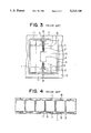
- FIGS. 3 and 4 show the configuration of a conventional leadframe.
- FIG. 3 shows a single conventional leadframe. Normally, a plurality of leadframes are formed in a strip, as shown in FIG. 4.
- a reference numeral 1 denotes a leadframe; 2, inner leads; 3, outer leads; 4, a die pad on which a semiconductor element (not shown) is mounted; 5, an outer frame portion of the leadframe 1; 6, hanging leads for connecting the die pad 4 to the outer frame portion 5; and 7, tie bars for preventing offset of the inner leads 2 and for preventing flow of a sealing resin to the outer leads 3 which are not packaged in the molding process.
- a reference numeral 8 denotes first positioning holes used for positioning the leadframe 1 with respect to the molding mold, tie bar cutting mold and lead forming mold (these molds being not shown) employed in the molding process, tie bar cutting process and outer lead forming process, respectively.
- the positioning holes 8 are formed in the outer frame portion 5 of the leadframe 1 at fixed intervals.
- the first positioning holes 8 are in general circular or elliptical.
- a reference numeral 9 denotes a resin injecting portion corresponding to a sub runner and a gate (both being not shown) which act as the flow passage of the molding resin in a molding mold. In the resin injecting portion, a plate on which the sealing resin flows extends from the outer frame portion 5 toward the center of the leadframe.
- a line 10 indicates a sealing line which is the contour of a molded resin which packages the leadframe 1.
- a line A in FIGS. 3 and 4 indicates a semiconductor device forming area including the inner leads 2, the outer leads 3, the die pad 4, the hanging leads 6 and the tie bars 7.
- a plurality of semiconductor device forming areas A are formed in series on a single leadframe strip 1, as shown in FIG. 4.
- a reference numeral 11 denotes slits for relieving distortion generated by the difference between the coefficient of thermal expansion between the leadframe 1 and of the molded resin when the molded resin is cooled from the molding temperature to room temperature, thereby preventing warpage of the semiconductor device caused by this distortion.
- the slits 11 are formed at the periphery of the semiconductor device forming areas A of the leadframe 1 except for the resin injecting portion 9, surrounding the semiconductor device forming area A.
- a semiconductor element (a chip) is first bonded to the die pad 4 using a resin bonding agent or solder.
- a large number of aluminum pad electrodes provided on the semiconductor element are respectively connected to the inner leads 2 using thin metal wires (not shown) made of gold, copper or aluminum.
- the leadframe 1 with the attached semiconductor elements thereon is placed in a mold (not shown), and a sealing resin is injected into the closed mold.
- armor processing is performed on the leadframe 1 using a solder plating, and thereafter the tie bars 7 are cut using a tie bar cutting mold.
- the outer leads 3 are bent in a predetermined shape using a lead forming mold, and at the same time the distal ends of the outer leads 3 are separated from the outer frame portion 5 of the leadframe 1, thereby completing manufacture of semiconductor devices.
- the positioning accuracy of the outer leads 3 deteriorates in the tie bar cutting process, because the first positioning holes 8 are located in the outer frame portion 5 separated from the rest of the leadframe by the slits 11. This position error may lead to erroneous cutting of the outer leads 3 during cutting of the tie bars 7.
- an object of the present invention is to provide a leadframe in which the positioning of the outer leads 3 is not affected by warpage and contraction of the leadframe 1 to improve the positioning accuracy of the outer leads 3 in the tie bar cutting process and thereby prevent cutting of the outer leads 3 and improve reliability of the semiconductor device.
- a leadframe used for the manufacture of semiconductor devices comprising a die pad on which a semiconductor element may be mounted, inner leads disposed around the die pad, outer leads, hanging leads supporting the die pad, tie bars connecting the outer leads and the hanging leads all disposed within a semiconductor device forming area of the leadframe; an outer frame integral with, supporting, and connected to the die pad and outer leads and disposed outside the semiconductor device forming area; a resin injecting portion extending from the outer frame portion toward the die pad for injecting a sealing resin; first positioning means for positioning the leadframe including a plurality of holes in the outer frame; and second positioning means in the vicinity of the tie bars and the outer leads for positioning the tie bars and the outer leads when the tie bars are cut.
- the outer leads can be positioned with a high degree of accuracy by means of the second positioning means provided in the vicinity of the outer leads during the tie bar cutting process.
- the second positioning means comprises positioning holes formed at three corners of a rectangle semiconductor device forming area in the vicinity of the tie bars but not at the fourth corner where resin injecting portion is disposed.
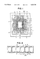
- FIG. 1 is an enlarged and plan view of a single leadframe according to an embodiment of the present invention
- FIG. 2 is a plan view showing a plurality of leadframe of FIG. 1;
- FIG. 3 is an enlarged and plan view of a conventional leadframe
- FIG. 4 is a plan view showing a plurality of leadframes of FIG. 3.
- FIGS. 1 and 2 An embodiment of the present invention will now be described with reference to FIGS. 1 and 2.
- FIGS. 1 and 2 respectively show an embodiment of a leadframe 100 according to the present invention.
- FIG. 1 shows a single leadframe according to an embodiment of the present invention. Normally, a plurality of leadframes are attached in a strips as shown in FIG. 2.
- FIGS. 1 and 2 the same reference numerals are used to denote parts and components which are the same as those shown in FIGS. 3 and 4, detailed description of the same parts being omitted.
- a reference numeral 21 denotes second positioning holes for positioning the leadframe 100, particularly, the semiconductor device forming area A in a tie bar cutting mold (not shown), during the tie bar 7 cutting process.
- the second positioning means includes second positioning holes.
- the three second positioning holes 21 are located at three corners of the semiconductor device forming area A but not at the corner where the resin injecting portion 9 is disposed in the vicinity of the tie bars 7 and outer leads 3.
- the three second positioning holes 21 are disposed at the same positions in each of the semiconductor device forming areas A.
- the three positioning holes 21 are each located where extensions of a longitudinal tie bar 7 intersect extensions of the lateral tie bar 7.
- the positioning holes 21 are each, in general circular.
- the outer leads 3 are positioned using the positioning holes 21 and the tie bars 7 are cut using the tie bar cutting mold (not shown) in the tie bar cutting process.
- assembly is conducted in the conventional manner using the first positioning holes 8.
- a leadframe with the slits 11 located around the semiconductor device forming area A have been described.
- the present invention can also be applied to a leadframe having no slits 11.
- a leadframe having the slits around the semiconductor device forming area and having positioning holes located inside the slits, i.e., at three corners of the semiconductor device forming area A, i.e., not at the corner where the resin injecting portion is formed, is known. These positioning holes absorb shift and distortion of the semiconductor device forming area A with respect to the outer frame portion of the leadframe, generated by the formation of the slits. These positioning holes are used in the sealing resin molding process, tie bar cutting process and outer lead forming process.
- the positioning holes according to the present invention are particularly formed for the purpose of improving the positioning accuracy of the outer leads in the tie bar cutting process, and are used to absorb a shift of the semiconductor device forming area A with respect to the outer frame portion of the leadframe as well as shift and distortion of the inner portion located inside the tie bars 7 or the mold line 10 shown in FIGS. 1 and 2 with respect to the semiconductor device forming area A. That is, the positioning holes according to the present invention are apparently formed for the purposes different from those of the conventional ones.
- the leadframe according to the present invention has second positioning means comprising three positioning holes formed in the vicinity of the tie bars on three corners of a rectangular semiconductor device forming area except for the corner where the resin injecting portion is provided.
- second positioning means comprising three positioning holes formed in the vicinity of the tie bars on three corners of a rectangular semiconductor device forming area except for the corner where the resin injecting portion is provided.
Abstract
Description
Claims (8)
Applications Claiming Priority (2)
| Application Number | Priority Date | Filing Date | Title |
|---|---|---|---|
| JP3-96474 | 1991-04-26 | ||
| JP3096474A JP2608192B2 (en) | 1991-04-26 | 1991-04-26 | Lead frame |
Publications (1)
| Publication Number | Publication Date |
|---|---|
| US5223738A true US5223738A (en) | 1993-06-29 |
Family
ID=14166046
Family Applications (1)
| Application Number | Title | Priority Date | Filing Date |
|---|---|---|---|
| US07/868,419 Expired - Lifetime US5223738A (en) | 1991-04-26 | 1992-04-15 | Leadframe |
Country Status (4)
| Country | Link |
|---|---|
| US (1) | US5223738A (en) |
| JP (1) | JP2608192B2 (en) |
| DE (1) | DE4213411A1 (en) |
| NL (1) | NL194456C (en) |
Cited By (13)
| Publication number | Priority date | Publication date | Assignee | Title |
|---|---|---|---|---|
| US5309018A (en) * | 1992-04-28 | 1994-05-03 | Rohm Co., Ltd. | Lead frame having deformable supports |
| US5338972A (en) * | 1992-08-10 | 1994-08-16 | Rohm Co., Ltd. | Lead frame with deformable buffer portions |
| US5517056A (en) * | 1993-09-30 | 1996-05-14 | Motorola, Inc. | Molded carrier ring leadframe having a particular resin injecting area design for gate removal and semiconductor device employing the same |
| US5763942A (en) * | 1995-08-16 | 1998-06-09 | Nec Corporation | Lead frame free of irregular deformation |
| US5766983A (en) * | 1994-04-29 | 1998-06-16 | Hewlett-Packard Company | Tape automated bonding circuit with interior sprocket holes |
| US5781682A (en) * | 1996-02-01 | 1998-07-14 | International Business Machines Corporation | Low-cost packaging for parallel optical computer link |
| US5929511A (en) * | 1996-07-15 | 1999-07-27 | Matsushita Electronics Corporation | Lead frame for resin sealed semiconductor device |
| US5939775A (en) * | 1996-11-05 | 1999-08-17 | Gcb Technologies, Llc | Leadframe structure and process for packaging intergrated circuits |
| US7291905B2 (en) * | 2000-08-08 | 2007-11-06 | Nec Electronics Corporation | Lead frame, semiconductor device produced by using the same and method of producing the semiconductor device |
| US20080199121A1 (en) * | 2005-09-30 | 2008-08-21 | Ntn Corporation | Bearing Apparatus for a Wheel of Vehicle |
| WO2016164876A1 (en) * | 2015-04-10 | 2016-10-13 | Texas Instruments Incorporated | Leadframe for electronic system having vertically stacked chips and components |
| EP3167253B1 (en) * | 2014-07-08 | 2019-03-20 | Continental Teves AG & Co. OHG | Vibration decoupling of sensors |
| US20190229044A1 (en) * | 2018-01-23 | 2019-07-25 | Nxp B.V. | Lead frame with plated lead tips |
Families Citing this family (1)
| Publication number | Priority date | Publication date | Assignee | Title |
|---|---|---|---|---|
| JP6389768B2 (en) * | 2015-01-23 | 2018-09-12 | 新日本無線株式会社 | Manufacturing method of circuit package with built-in lead |
Citations (9)
| Publication number | Priority date | Publication date | Assignee | Title |
|---|---|---|---|---|
| US4477827A (en) * | 1981-02-02 | 1984-10-16 | Northern Telecom Limited | Lead frame for leaded semiconductor chip carriers |
| US4496965A (en) * | 1981-05-18 | 1985-01-29 | Texas Instruments Incorporated | Stacked interdigitated lead frame assembly |
| JPH01165057A (en) * | 1987-12-21 | 1989-06-29 | Toshiba Corp | Tape cassette classification detector |
| US4868635A (en) * | 1988-01-13 | 1989-09-19 | Texas Instruments Incorporated | Lead frame for integrated circuit |
| US4870474A (en) * | 1986-12-12 | 1989-09-26 | Texas Instruments Incorporated | Lead frame |
| US4920074A (en) * | 1987-02-25 | 1990-04-24 | Hitachi, Ltd. | Surface mount plastic package semiconductor integrated circuit, manufacturing method thereof, as well as mounting method and mounted structure thereof |
| US4977442A (en) * | 1988-02-24 | 1990-12-11 | Fujitsu Limited | Lead frame and method of producing electronic components using such improved lead frame |
| US5031022A (en) * | 1989-05-02 | 1991-07-09 | Nippon Steel Corporation | Film carrier for mounting IC chips |
| US5057901A (en) * | 1989-09-27 | 1991-10-15 | Die Tech, Inc. | Lead frame for semi-conductor device |
Family Cites Families (10)
| Publication number | Priority date | Publication date | Assignee | Title |
|---|---|---|---|---|
| JPS5521128A (en) * | 1978-08-02 | 1980-02-15 | Hitachi Ltd | Lead frame used for semiconductor device and its assembling |
| DE3379882D1 (en) * | 1982-03-02 | 1989-06-22 | Siemens Ag | Film carrier for an electrical conductor pattern |
| US4918511A (en) * | 1985-02-01 | 1990-04-17 | Advanced Micro Devices, Inc. | Thermal expansion compensated metal lead frame for integrated circuit package |
| JPS62234337A (en) * | 1986-04-04 | 1987-10-14 | Hitachi Cable Ltd | Film carrier for semiconductor device |
| DE3635375A1 (en) * | 1986-10-17 | 1988-04-28 | Heraeus Gmbh W C | Lead frame for electronic components |
| JP2671900B2 (en) * | 1987-03-06 | 1997-11-05 | 沖電気工業株式会社 | Lead frame for semiconductor device |
| JPH01145839A (en) * | 1987-12-02 | 1989-06-07 | Rhythm Watch Co Ltd | Lead frame |
| JPH02232957A (en) * | 1989-03-06 | 1990-09-14 | Yamada Seisakusho:Kk | Lead frame of resin sealed type semiconductor device |
| JPH02266550A (en) * | 1989-04-07 | 1990-10-31 | Sharp Corp | Surface mounting type ic package |
| JPH0479358A (en) * | 1990-07-23 | 1992-03-12 | Nec Corp | Lead frame for semiconductor device |
-
1991
- 1991-04-26 JP JP3096474A patent/JP2608192B2/en not_active Expired - Fee Related
-
1992
- 1992-04-15 US US07/868,419 patent/US5223738A/en not_active Expired - Lifetime
- 1992-04-21 NL NL9200722A patent/NL194456C/en not_active IP Right Cessation
- 1992-04-23 DE DE4213411A patent/DE4213411A1/en not_active Ceased
Patent Citations (9)
| Publication number | Priority date | Publication date | Assignee | Title |
|---|---|---|---|---|
| US4477827A (en) * | 1981-02-02 | 1984-10-16 | Northern Telecom Limited | Lead frame for leaded semiconductor chip carriers |
| US4496965A (en) * | 1981-05-18 | 1985-01-29 | Texas Instruments Incorporated | Stacked interdigitated lead frame assembly |
| US4870474A (en) * | 1986-12-12 | 1989-09-26 | Texas Instruments Incorporated | Lead frame |
| US4920074A (en) * | 1987-02-25 | 1990-04-24 | Hitachi, Ltd. | Surface mount plastic package semiconductor integrated circuit, manufacturing method thereof, as well as mounting method and mounted structure thereof |
| JPH01165057A (en) * | 1987-12-21 | 1989-06-29 | Toshiba Corp | Tape cassette classification detector |
| US4868635A (en) * | 1988-01-13 | 1989-09-19 | Texas Instruments Incorporated | Lead frame for integrated circuit |
| US4977442A (en) * | 1988-02-24 | 1990-12-11 | Fujitsu Limited | Lead frame and method of producing electronic components using such improved lead frame |
| US5031022A (en) * | 1989-05-02 | 1991-07-09 | Nippon Steel Corporation | Film carrier for mounting IC chips |
| US5057901A (en) * | 1989-09-27 | 1991-10-15 | Die Tech, Inc. | Lead frame for semi-conductor device |
Cited By (18)
| Publication number | Priority date | Publication date | Assignee | Title |
|---|---|---|---|---|
| US5309018A (en) * | 1992-04-28 | 1994-05-03 | Rohm Co., Ltd. | Lead frame having deformable supports |
| US5338972A (en) * | 1992-08-10 | 1994-08-16 | Rohm Co., Ltd. | Lead frame with deformable buffer portions |
| US5517056A (en) * | 1993-09-30 | 1996-05-14 | Motorola, Inc. | Molded carrier ring leadframe having a particular resin injecting area design for gate removal and semiconductor device employing the same |
| US5766983A (en) * | 1994-04-29 | 1998-06-16 | Hewlett-Packard Company | Tape automated bonding circuit with interior sprocket holes |
| US5763942A (en) * | 1995-08-16 | 1998-06-09 | Nec Corporation | Lead frame free of irregular deformation |
| US6137158A (en) * | 1996-02-01 | 2000-10-24 | International Business Machines Corporation | Leadframe and leadframe assembly for parallel optical computer link |
| US5781682A (en) * | 1996-02-01 | 1998-07-14 | International Business Machines Corporation | Low-cost packaging for parallel optical computer link |
| US5929511A (en) * | 1996-07-15 | 1999-07-27 | Matsushita Electronics Corporation | Lead frame for resin sealed semiconductor device |
| US5939775A (en) * | 1996-11-05 | 1999-08-17 | Gcb Technologies, Llc | Leadframe structure and process for packaging intergrated circuits |
| US7291905B2 (en) * | 2000-08-08 | 2007-11-06 | Nec Electronics Corporation | Lead frame, semiconductor device produced by using the same and method of producing the semiconductor device |
| US20080199121A1 (en) * | 2005-09-30 | 2008-08-21 | Ntn Corporation | Bearing Apparatus for a Wheel of Vehicle |
| EP3167253B1 (en) * | 2014-07-08 | 2019-03-20 | Continental Teves AG & Co. OHG | Vibration decoupling of sensors |
| US11118908B2 (en) | 2014-07-08 | 2021-09-14 | Continental Teves Ag & Co. Ohg | Structure-borne noise decoupling on sensors working with transmitter fields |
| WO2016164876A1 (en) * | 2015-04-10 | 2016-10-13 | Texas Instruments Incorporated | Leadframe for electronic system having vertically stacked chips and components |
| US9496206B2 (en) | 2015-04-10 | 2016-11-15 | Texas Instruments Incorporated | Flippable leadframe for packaged electronic system having vertically stacked chips and components |
| US10879154B2 (en) | 2015-04-10 | 2020-12-29 | Texas Instruments Incorporated | Flippable leadframe for packaged electronic system having vertically stacked chips and components |
| US11742263B2 (en) | 2015-04-10 | 2023-08-29 | Texas Instruments Incorporated | Flippable leadframe for packaged electronic system having vertically stacked chip and components |
| US20190229044A1 (en) * | 2018-01-23 | 2019-07-25 | Nxp B.V. | Lead frame with plated lead tips |
Also Published As
| Publication number | Publication date |
|---|---|
| JPH04326561A (en) | 1992-11-16 |
| DE4213411A1 (en) | 1992-10-29 |
| NL9200722A (en) | 1992-11-16 |
| NL194456C (en) | 2002-04-04 |
| JP2608192B2 (en) | 1997-05-07 |
| NL194456B (en) | 2001-12-03 |
Similar Documents
| Publication | Publication Date | Title |
|---|---|---|
| US10490486B2 (en) | Semiconductor device | |
| US6281566B1 (en) | Plastic package for electronic devices | |
| US5223738A (en) | Leadframe | |
| JPH0783036B2 (en) | Carrier tape | |
| US20020056905A1 (en) | Semiconductor device and method of fabricating the same | |
| KR0141952B1 (en) | Semiconductor package and production thereof | |
| US20030003629A1 (en) | Hybrid integrated circuit device and manufacturing method thereof | |
| US5623163A (en) | Leadframe for semiconductor devices | |
| KR100454774B1 (en) | Semiconductor device | |
| JP3036339B2 (en) | Semiconductor device | |
| WO1986002200A1 (en) | Lead frame having improved arrangement of supporting leads and semiconductor device employing the same | |
| KR19990034731A (en) | Lead-on chip lead frames and packages using them | |
| JPH0719870B2 (en) | Lead frame | |
| KR0119759Y1 (en) | Bottom Leaded Semiconductor Package | |
| JPH03165057A (en) | Lead frame | |
| JP2515882B2 (en) | Lead frame, method of manufacturing lead frame, semiconductor device, and method of manufacturing semiconductor device | |
| JPH03102859A (en) | Manufacturing method of semiconductor device | |
| JPH04316359A (en) | Lead frame and manufacture of semiconductor device using same | |
| JPH08204101A (en) | Lead frame for semiconductor device | |
| JPH0992766A (en) | Lead frame and manufacturing method for semiconductor device using it | |
| JPH06216289A (en) | Formation of plastic sealed semiconductor device | |
| KR980012344A (en) | Semiconductor chip package for improved fluidity | |
| JPH01207936A (en) | Manufacture of resin-sealed semiconductor device | |
| KR970013264A (en) | Leadframe of Semiconductor Chip Package | |
| KR19990039829A (en) | Lead frame and semiconductor package using same |
Legal Events
| Date | Code | Title | Description |
|---|---|---|---|
| AS | Assignment |
Owner name: MITSUBISHI DENKI KABUSHIKI KAISHA, JAPAN Free format text: ASSIGNMENT OF ASSIGNORS INTEREST.;ASSIGNOR:OKADA, MAKIO;REEL/FRAME:006102/0084 Effective date: 19920327 |
|
| STCF | Information on status: patent grant |
Free format text: PATENTED CASE |
|
| FEPP | Fee payment procedure |
Free format text: PAYOR NUMBER ASSIGNED (ORIGINAL EVENT CODE: ASPN); ENTITY STATUS OF PATENT OWNER: LARGE ENTITY |
|
| FPAY | Fee payment |
Year of fee payment: 4 |
|
| FPAY | Fee payment |
Year of fee payment: 8 |
|
| FPAY | Fee payment |
Year of fee payment: 12 |
|
| AS | Assignment |
Owner name: RENESAS ELECTRONICS CORPORATION, JAPAN Free format text: ASSIGNMENT OF ASSIGNORS INTEREST;ASSIGNOR:MITSUBISHI DENKI KABUSHIKI KAISHA;REEL/FRAME:025980/0219 Effective date: 20110307 |