US5197902A - Termination adaptor connector device - Google Patents
Termination adaptor connector device Download PDFInfo
- Publication number
- US5197902A US5197902A US07/705,653 US70565391A US5197902A US 5197902 A US5197902 A US 5197902A US 70565391 A US70565391 A US 70565391A US 5197902 A US5197902 A US 5197902A
- Authority
- US
- United States
- Prior art keywords
- connector
- printed circuit
- flexible printed
- conductive
- loop
- Prior art date
- Legal status (The legal status is an assumption and is not a legal conclusion. Google has not performed a legal analysis and makes no representation as to the accuracy of the status listed.)
- Expired - Fee Related
Links
Images


Classifications
-
- H—ELECTRICITY
- H05—ELECTRIC TECHNIQUES NOT OTHERWISE PROVIDED FOR
- H05K—PRINTED CIRCUITS; CASINGS OR CONSTRUCTIONAL DETAILS OF ELECTRIC APPARATUS; MANUFACTURE OF ASSEMBLAGES OF ELECTRICAL COMPONENTS
- H05K1/00—Printed circuits
- H05K1/02—Details
- H05K1/11—Printed elements for providing electric connections to or between printed circuits
- H05K1/118—Printed elements for providing electric connections to or between printed circuits specially for flexible printed circuits, e.g. using folded portions
-
- H—ELECTRICITY
- H01—ELECTRIC ELEMENTS
- H01R—ELECTRICALLY-CONDUCTIVE CONNECTIONS; STRUCTURAL ASSOCIATIONS OF A PLURALITY OF MUTUALLY-INSULATED ELECTRICAL CONNECTING ELEMENTS; COUPLING DEVICES; CURRENT COLLECTORS
- H01R12/00—Structural associations of a plurality of mutually-insulated electrical connecting elements, specially adapted for printed circuits, e.g. printed circuit boards [PCB], flat or ribbon cables, or like generally planar structures, e.g. terminal strips, terminal blocks; Coupling devices specially adapted for printed circuits, flat or ribbon cables, or like generally planar structures; Terminals specially adapted for contact with, or insertion into, printed circuits, flat or ribbon cables, or like generally planar structures
- H01R12/50—Fixed connections
- H01R12/59—Fixed connections for flexible printed circuits, flat or ribbon cables or like structures
- H01R12/65—Fixed connections for flexible printed circuits, flat or ribbon cables or like structures characterised by the terminal
- H01R12/67—Fixed connections for flexible printed circuits, flat or ribbon cables or like structures characterised by the terminal insulation penetrating terminals
- H01R12/675—Fixed connections for flexible printed circuits, flat or ribbon cables or like structures characterised by the terminal insulation penetrating terminals with contacts having at least a slotted plate for penetration of cable insulation, e.g. insulation displacement contacts for round conductor flat cables
-
- H—ELECTRICITY
- H05—ELECTRIC TECHNIQUES NOT OTHERWISE PROVIDED FOR
- H05K—PRINTED CIRCUITS; CASINGS OR CONSTRUCTIONAL DETAILS OF ELECTRIC APPARATUS; MANUFACTURE OF ASSEMBLAGES OF ELECTRICAL COMPONENTS
- H05K3/00—Apparatus or processes for manufacturing printed circuits
- H05K3/30—Assembling printed circuits with electric components, e.g. with resistors
- H05K3/32—Assembling printed circuits with electric components, e.g. with resistors electrically connecting electric components or wires to printed circuits
- H05K3/325—Assembling printed circuits with electric components, e.g. with resistors electrically connecting electric components or wires to printed circuits by abutting or pinching; Mechanical auxiliary parts therefor
- H05K3/326—Assembling printed circuits with electric components, e.g. with resistors electrically connecting electric components or wires to printed circuits by abutting or pinching; Mechanical auxiliary parts therefor the printed circuit having integral resilient or deformable parts, e.g. tabs or parts of flexible circuits
-
- H—ELECTRICITY
- H01—ELECTRIC ELEMENTS
- H01R—ELECTRICALLY-CONDUCTIVE CONNECTIONS; STRUCTURAL ASSOCIATIONS OF A PLURALITY OF MUTUALLY-INSULATED ELECTRICAL CONNECTING ELEMENTS; COUPLING DEVICES; CURRENT COLLECTORS
- H01R13/00—Details of coupling devices of the kinds covered by groups H01R12/70 or H01R24/00 - H01R33/00
- H01R13/66—Structural association with built-in electrical component
-
- H—ELECTRICITY
- H05—ELECTRIC TECHNIQUES NOT OTHERWISE PROVIDED FOR
- H05K—PRINTED CIRCUITS; CASINGS OR CONSTRUCTIONAL DETAILS OF ELECTRIC APPARATUS; MANUFACTURE OF ASSEMBLAGES OF ELECTRICAL COMPONENTS
- H05K1/00—Printed circuits
- H05K1/02—Details
- H05K1/03—Use of materials for the substrate
- H05K1/0393—Flexible materials
-
- H—ELECTRICITY
- H05—ELECTRIC TECHNIQUES NOT OTHERWISE PROVIDED FOR
- H05K—PRINTED CIRCUITS; CASINGS OR CONSTRUCTIONAL DETAILS OF ELECTRIC APPARATUS; MANUFACTURE OF ASSEMBLAGES OF ELECTRICAL COMPONENTS
- H05K1/00—Printed circuits
- H05K1/02—Details
- H05K1/09—Use of materials for the conductive, e.g. metallic pattern
- H05K1/092—Dispersed materials, e.g. conductive pastes or inks
- H05K1/095—Dispersed materials, e.g. conductive pastes or inks for polymer thick films, i.e. having a permanent organic polymeric binder
-
- H—ELECTRICITY
- H05—ELECTRIC TECHNIQUES NOT OTHERWISE PROVIDED FOR
- H05K—PRINTED CIRCUITS; CASINGS OR CONSTRUCTIONAL DETAILS OF ELECTRIC APPARATUS; MANUFACTURE OF ASSEMBLAGES OF ELECTRICAL COMPONENTS
- H05K1/00—Printed circuits
- H05K1/18—Printed circuits structurally associated with non-printed electric components
- H05K1/189—Printed circuits structurally associated with non-printed electric components characterised by the use of flexible or folded printed circuits
-
- H—ELECTRICITY
- H05—ELECTRIC TECHNIQUES NOT OTHERWISE PROVIDED FOR
- H05K—PRINTED CIRCUITS; CASINGS OR CONSTRUCTIONAL DETAILS OF ELECTRIC APPARATUS; MANUFACTURE OF ASSEMBLAGES OF ELECTRICAL COMPONENTS
- H05K2201/00—Indexing scheme relating to printed circuits covered by H05K1/00
- H05K2201/04—Assemblies of printed circuits
- H05K2201/042—Stacked spaced PCBs; Planar parts of folded flexible circuits having mounted components in between or spaced from each other
-
- H—ELECTRICITY
- H05—ELECTRIC TECHNIQUES NOT OTHERWISE PROVIDED FOR
- H05K—PRINTED CIRCUITS; CASINGS OR CONSTRUCTIONAL DETAILS OF ELECTRIC APPARATUS; MANUFACTURE OF ASSEMBLAGES OF ELECTRICAL COMPONENTS
- H05K2201/00—Indexing scheme relating to printed circuits covered by H05K1/00
- H05K2201/09—Shape and layout
- H05K2201/09009—Substrate related
- H05K2201/09063—Holes or slots in insulating substrate not used for electrical connections
-
- H—ELECTRICITY
- H05—ELECTRIC TECHNIQUES NOT OTHERWISE PROVIDED FOR
- H05K—PRINTED CIRCUITS; CASINGS OR CONSTRUCTIONAL DETAILS OF ELECTRIC APPARATUS; MANUFACTURE OF ASSEMBLAGES OF ELECTRICAL COMPONENTS
- H05K2201/00—Indexing scheme relating to printed circuits covered by H05K1/00
- H05K2201/10—Details of components or other objects attached to or integrated in a printed circuit board
- H05K2201/10613—Details of electrical connections of non-printed components, e.g. special leads
- H05K2201/10621—Components characterised by their electrical contacts
- H05K2201/10689—Leaded Integrated Circuit [IC] package, e.g. dual-in-line [DIL]
-
- H—ELECTRICITY
- H05—ELECTRIC TECHNIQUES NOT OTHERWISE PROVIDED FOR
- H05K—PRINTED CIRCUITS; CASINGS OR CONSTRUCTIONAL DETAILS OF ELECTRIC APPARATUS; MANUFACTURE OF ASSEMBLAGES OF ELECTRICAL COMPONENTS
- H05K3/00—Apparatus or processes for manufacturing printed circuits
- H05K3/30—Assembling printed circuits with electric components, e.g. with resistors
- H05K3/32—Assembling printed circuits with electric components, e.g. with resistors electrically connecting electric components or wires to printed circuits
- H05K3/34—Assembling printed circuits with electric components, e.g. with resistors electrically connecting electric components or wires to printed circuits by soldering
- H05K3/341—Surface mounted components
- H05K3/3421—Leaded components
-
- H—ELECTRICITY
- H05—ELECTRIC TECHNIQUES NOT OTHERWISE PROVIDED FOR
- H05K—PRINTED CIRCUITS; CASINGS OR CONSTRUCTIONAL DETAILS OF ELECTRIC APPARATUS; MANUFACTURE OF ASSEMBLAGES OF ELECTRICAL COMPONENTS
- H05K3/00—Apparatus or processes for manufacturing printed circuits
- H05K3/46—Manufacturing multilayer circuits
- H05K3/4685—Manufacturing of cross-over conductors
Definitions
- the present invention relates to a termination adaptor connector, including among other elements a package or housing.
- a connector of a first type is accommodated in the housing and intended to be connected to the end of a line over which signals travel of an electronic system having a connector of a second type, for adapting the line and/or simulating the connection between the line and an external device effectively accommodated in the package.
- Means for supporting and linking adaptation and/or simulation elements is connected to the connector of the first type.
- Termination adaptor connectors are currently used to test or adapt an electronic system, or to simulate its connection to some other electronic system. Examples of such devices may be found in electronic components catalogs, more particularly for connectors, published by the manufacturers, such as 3M or AMP. To terminate a line, it is presently usual to use small-sized connector packages, which may include jumper links, electric wires, or adaptation resistors. However, if integration with the connector packages of circuits or bulkier elements is desired, then rigid printed circuits welded to the connectors are used, and the bulky elements are disposed on these circuits. Taking into account the relative bulk of the printed circuit and the elements carried by it, this necessitates the use of equally bulky connector packages, which may have serious disadvantages.
- the object of the present invention is to effectively overcome the various disadvantages discussed above, by a device that is very simple to use, offers very good performance, and is of reduced cost.
- the termination adaptor connector of the present invention is notable in that the support and linking means is a flexible printed circuit. Linkage between the connector of the first type and the flexible printed circuit is obtained by means of slit self-stripping connections carried by the connector, which perforate the insulation, when present, of the flexible printed circuit and clasp or capture the conductive ends of the flexible printed circuit, which are especially adapted to this end, in the slits provided in the self-stripping connections.
- the concept of the invention is to use a flexible printed circuit, which by its flexibility makes it possible, in the simplest possible manner, to fully utilize the volume inside the connector package while effectively supporting even bulky elements. Implementation of this concept thus achieves a very significant gain in space. Furthermore, in association with the flexible printed circuit, the self-stripping connections allow easy, heavyduty use, and the risk of circuit detachment is averted, since no other welding is necessary. Finally, effective shielding can be attained without difficulty and without increasing the volume, because of the use of a flexible printed circuit, taking into account its intrinsic properties on the one hand and on the other hand the fact that ground planes or lines can be easily integrated into the thickness of the insulator when the printed circuit is made.
- the conductive ends of the flexible printed circuit are remarkable in that they are not covered with insulation and they have a predetermined width, as a function of the width of the slits of the self-stripping connections.
- the width of the conductive ends are slightly greater than the width of the slits, so as to assure a forced connection when the connections pierce the flexible printed circuit.
- each self-stripping connection perforates the insulation, if any, on either side of this conductive end, while the conductive end is clasped and captured, and can perfectly match the shape of the slit.
- the ends of the flexible printed circuit are remarkable in that they have a thickness that is at least twice as great as the thickness of the other conductive portions of the flexible printed circuit.
- At least two conductive ends which may or may not be adjacent, can be connected to one another by means of conductive ink and metallized holes.
- the conductive ink may be disposed in the thickness of the insulator transversely to the conductive lines, while the linkage between conductive lines and conductive ink is obtained selectively by means of selective placement of metallized holes. This makes it easy to make a linkage between lines and also to further improve the shielding when a plurality of ground lines are connected to one another at a common point just upstream of the conductive ends.
- the flexible printed circuit may also form a loop, the two ends of which are connected to the connector. This makes it possible to insert the adaptation and/or simulation elements inside the loop, which may also have the effect of improving shielding while guaranteeing a major gain in space and great ease of insertion into the package.
- the flexible printed circuit when it has the shape of a loop, may be provided with two transverse cutouts along the same axis, on either side of its median portion, each cutout extending over approximately one-third the width of the flexible printed circuit and ending inside the circuit in a circular recess, in such a manner as to avert any extension of the transverse cutouts.
- the flexible printed circuit is provided with conductor sites that are not covered with insulation, making it easier to affix the adaptation or simulation elements by means of soldering.
- the conductive ends and the conductor sites not covered with insulation of the flexible printed circuit may be protected at the time of manufacture by an antioxidant compound, for example, an alloy of lead and tin deposited by tinning.
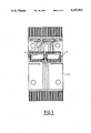
- FIG. 1a shows an example of the termination adaptor connector according to the invention
- FIG. 1b shows a detail relating to the linkage between a flexible printed circuit and a self-stripping connection.
- FIG. 2a shows one exemplary embodiment of a flexible printed circuit
- FIGS. 2b and 2c show details of a circled portion of the embodiment of an outlined portion of FIG. 2a
- FIG. 3 shows an embodiment of the flexible printed circuit provided with adaptation and/or simulation elements.
- FIG. 1a proposes an exemplary, non-limiting embodiment of a termination adaptor connector, for which the concept of the invention is used and implemented.
- the connector device includes a connector package or housing 1 comprising an upper portion and a lower portion.
- Housing 1 may be any commercially available package. Use of commercially prefabricated housings has the advantage of avoiding special adaptation or machining of this part.
- Accommodated in the package is a connector 2 of a first type (for instance, female), intended to be connected to the end of a line of an electronic system having a connector (not shown) of a second type (for example, male, if the connector of the first type is female), over which signals pass, for adapting this line and/or simulating its connection to an external device.
- a connector 2 of a first type for instance, female
- a connector not shown
- a second type for example, male, if the connector of the first type is female
- signals pass for adapting this line and/or simulating its connection to an external device.
- the support and linkage means 3 is a flexible printed circuit, the linkage of which with the connector 2 is obtained by means of self-stripping slit connections 6 carried by the connector 2 (for example, self-stripping connections made by the 3M Corporation).
- a self-stripping connection 6 perforates the insulation 30 (which is present in this particular example) of the flexible printed circuit 3 and clasps the conductive end 31 of the flexible printed circuit 3 in the U-shaped slit 60, this end 31 being especially adapted for this purpose.
- the conductive ends 31 of the flexible printed circuit 3 are not covered with insulation and have a predetermined width, as a function of the width of the slits of the self-stripping connections 6 and hence as a function of which such connections are selected.
- the width of the conductive ends must be slightly greater than the width of the U-shaped slits, to assure a forced connection when the connection comes to clasp the conductive end in its slit, which consequently guarantees high-quality contact and also serves to capture or imprison the conductive end.
- FIG. 2a shows an exemplary embodiment of a flexible printed circuit, the insulation of which may comprise Kapton (trademark registered by E. I. DuPont de Nemours and Company), Upilex (trademark registered by Ube Industries, Inc.), or any other material having similar characteristics.
- the flexible printed circuit comprises copper links or tracks, having a thickness of approximately 100 ⁇ m, covered with one or more insulating layers on both sides. These copper tracks make it possible to connect the adaptation and/or simulation elements (see FIG. 3) to the conductive ends 31.
- each conductive end of the flexible printed circuit 3 may have a thickness at least twice as great, for example, being on the order of 250 ⁇ m, as the thickness of the other conductive parts (the thicknesses of which are approximately 100 ⁇ m) of the circuit 3. Furthermore, it can be seen that as has been noted above, the conductive ends 31 are not covered with insulation.
- FIGS. 2b and 2c also make it possible to see how two conductive ends 31, which may or may not be adjacent (in FIG. 2b, they are not adjacent), may be connected to one another by means of a linkage of conductive ink 33 and metallized holes 34.
- the conductive ink is disposed in the thickness of the insulator (in FIG. 2c, it is disposed between two insulation layers 35) transversely to the conductor lines 36, while the linkage between conductor lines 36 and conductive ink 33 is selectively obtained by means of metallized holes 34.
- a layer of conductive ink may be made, for example, by screenprinting using an ink that contains silver.
- the flexible printed circuit 3 forms a loop, shown in FIG. 1a, the two ends of which, comprising the conductive ends 31a and 31b, are connected to the connector 2 (FIG. 1a) by means of connections 6.
- this circuit 3 is provided with two transverse cutouts 37 on either side of its middle portion and extending along the same axis xx', each cutout extending over approximately one-third the width of the flexible printed circuit 3 and ending inside the circuit in a circular recess 370.
- the flexible printed circuit 3 is provided with conductor sites 38 that are exposed and not covered with insulation. These sites are provided to receive the adaptation and/or simulation elements, such as those described in conjunction with FIG. 3.
- the conductor sites 38 and the conductive ends 31a and 31b may furthermore be protected with an antioxidant compound 39, for example, an alloy of lead and tin that is deposited by tinning at the time the circuit 3 is manufactured, and the thickness of which may be approximately 10 ⁇ m.
- the flexible circuit 3 as described in conjunction with FIGS. 2a, 2b, 2c, is shown provided with adaptation and simulation elements 4, which in this exemplary embodiment may be two integrated circuits such as a Texas Instruments ULN 2003D chip, a Motorola MC 1413 D chip, or any equivalent, each including a plurality of npn transistors each equipped with a base resistor and organized in such a manner as to form Darlington assemblies.
- a termination adaptor connector of this kind makes it possible to adapt and simulate a printer, for instance, at the output of a computer.
- the device because of the increase in space gained by the device according to the invention, it can advantageously be used when the adaptation and/or simulation elements, such as integrated circuits, to be inserted into it are very bulky, and when the space for receiving them is limited. Its cost is less, because a commercially available package can be used without having to be adapted, and it does not require the implementation of complex techniques; on the contrary, it is easy to use. Moreover, it makes it possible to improve shielding in a simple manner, without increasing the volume.
Landscapes
- Engineering & Computer Science (AREA)
- Microelectronics & Electronic Packaging (AREA)
- Metallurgy (AREA)
- Manufacturing & Machinery (AREA)
- Coupling Device And Connection With Printed Circuit (AREA)
- Multi-Conductor Connections (AREA)
- Details Of Connecting Devices For Male And Female Coupling (AREA)
- Structure Of Printed Boards (AREA)
Applications Claiming Priority (2)
| Application Number | Priority Date | Filing Date | Title |
|---|---|---|---|
| FR9006692 | 1990-05-30 | ||
| FR9006692A FR2662863B1 (fr) | 1990-05-30 | 1990-05-30 | Dispositif connecteur adaptateur de terminaison. |
Publications (1)
| Publication Number | Publication Date |
|---|---|
| US5197902A true US5197902A (en) | 1993-03-30 |
Family
ID=9397076
Family Applications (1)
| Application Number | Title | Priority Date | Filing Date |
|---|---|---|---|
| US07/705,653 Expired - Fee Related US5197902A (en) | 1990-05-30 | 1991-05-24 | Termination adaptor connector device |
Country Status (6)
| Country | Link |
|---|---|
| US (1) | US5197902A (de) |
| EP (1) | EP0459876B1 (de) |
| CA (1) | CA2043359C (de) |
| DE (1) | DE69105042T2 (de) |
| ES (1) | ES2067174T3 (de) |
| FR (1) | FR2662863B1 (de) |
Cited By (6)
| Publication number | Priority date | Publication date | Assignee | Title |
|---|---|---|---|---|
| EP0723710A4 (de) * | 1993-08-20 | 1997-07-09 | Berg Tech Inc | Elektrische verbindungsanordnung |
| US5895278A (en) * | 1996-10-10 | 1999-04-20 | Thomas & Betts Corporation | Controlled impedance, high density electrical connector |
| US6224395B1 (en) * | 1997-05-28 | 2001-05-01 | International Business Machines Corporation | Flex cables with increased three-dimensional conformity and design flexibility |
| US6320137B1 (en) * | 2000-04-11 | 2001-11-20 | 3M Innovative Properties Company | Flexible circuit with coverplate layer and overlapping protective layer |
| US8517759B1 (en) * | 2011-02-15 | 2013-08-27 | Blue Sun Energy, Inc. | Ribbon flex light connector system |
| US20180343740A1 (en) * | 2016-02-24 | 2018-11-29 | Murata Manufacturing Co., Ltd. | Composite substrate, method of manufacturing composite substrate, and method of manufacturing flexible board |
Families Citing this family (1)
| Publication number | Priority date | Publication date | Assignee | Title |
|---|---|---|---|---|
| KR100733877B1 (ko) * | 2000-07-06 | 2007-07-02 | 엘지.필립스 엘시디 주식회사 | 가요성 인쇄회로 필름 |
Citations (10)
| Publication number | Priority date | Publication date | Assignee | Title |
|---|---|---|---|---|
| CA669570A (en) * | 1963-08-27 | W. Allen Clifford | Electro-pneumatic translator | |
| US3335393A (en) * | 1964-12-16 | 1967-08-08 | United Carr Inc | Electrical connector |
| US3359529A (en) * | 1966-05-06 | 1967-12-19 | United Carr Inc | Electrical connector assembly |
| US4418239A (en) * | 1981-08-24 | 1983-11-29 | Oak Industries Inc. | Flexible connector with interconnection between conductive traces |
| US4573752A (en) * | 1984-04-04 | 1986-03-04 | Parlex Corporation | Flat cable connection system |
| FR2577353A1 (fr) * | 1985-02-13 | 1986-08-14 | Constr Telephoniques | Agencement pour l'insertion d'un support souple dans un connecteur encartable |
| EP0259082A2 (de) * | 1986-08-28 | 1988-03-09 | Minnesota Mining And Manufacturing Company | Integral geformter Kabelendenzusammenbau, Kontakt und Methode |
| FR2613539A1 (fr) * | 1987-04-03 | 1988-10-07 | Bull Sa | Connecteur de bus adapte en impedance et procede de fabrication d'un tel connecteur |
| US4902236A (en) * | 1988-11-14 | 1990-02-20 | E. I. Du Pont De Nemours And Company | Flex circuit and cable assembly |
| US4913656A (en) * | 1989-04-07 | 1990-04-03 | Rogers Corporation | Electrical connector |
-
1990
- 1990-05-30 FR FR9006692A patent/FR2662863B1/fr not_active Expired - Lifetime
-
1991
- 1991-05-23 EP EP91401335A patent/EP0459876B1/de not_active Expired - Lifetime
- 1991-05-23 ES ES91401335T patent/ES2067174T3/es not_active Expired - Lifetime
- 1991-05-23 DE DE69105042T patent/DE69105042T2/de not_active Expired - Fee Related
- 1991-05-24 US US07/705,653 patent/US5197902A/en not_active Expired - Fee Related
- 1991-05-28 CA CA002043359A patent/CA2043359C/fr not_active Expired - Fee Related
Patent Citations (10)
| Publication number | Priority date | Publication date | Assignee | Title |
|---|---|---|---|---|
| CA669570A (en) * | 1963-08-27 | W. Allen Clifford | Electro-pneumatic translator | |
| US3335393A (en) * | 1964-12-16 | 1967-08-08 | United Carr Inc | Electrical connector |
| US3359529A (en) * | 1966-05-06 | 1967-12-19 | United Carr Inc | Electrical connector assembly |
| US4418239A (en) * | 1981-08-24 | 1983-11-29 | Oak Industries Inc. | Flexible connector with interconnection between conductive traces |
| US4573752A (en) * | 1984-04-04 | 1986-03-04 | Parlex Corporation | Flat cable connection system |
| FR2577353A1 (fr) * | 1985-02-13 | 1986-08-14 | Constr Telephoniques | Agencement pour l'insertion d'un support souple dans un connecteur encartable |
| EP0259082A2 (de) * | 1986-08-28 | 1988-03-09 | Minnesota Mining And Manufacturing Company | Integral geformter Kabelendenzusammenbau, Kontakt und Methode |
| FR2613539A1 (fr) * | 1987-04-03 | 1988-10-07 | Bull Sa | Connecteur de bus adapte en impedance et procede de fabrication d'un tel connecteur |
| US4902236A (en) * | 1988-11-14 | 1990-02-20 | E. I. Du Pont De Nemours And Company | Flex circuit and cable assembly |
| US4913656A (en) * | 1989-04-07 | 1990-04-03 | Rogers Corporation | Electrical connector |
Cited By (8)
| Publication number | Priority date | Publication date | Assignee | Title |
|---|---|---|---|---|
| EP0723710A4 (de) * | 1993-08-20 | 1997-07-09 | Berg Tech Inc | Elektrische verbindungsanordnung |
| US5895278A (en) * | 1996-10-10 | 1999-04-20 | Thomas & Betts Corporation | Controlled impedance, high density electrical connector |
| US6053751A (en) * | 1996-10-10 | 2000-04-25 | Thomas & Betts Corporation | Controlled impedance, high density electrical connector |
| US6224395B1 (en) * | 1997-05-28 | 2001-05-01 | International Business Machines Corporation | Flex cables with increased three-dimensional conformity and design flexibility |
| US6320137B1 (en) * | 2000-04-11 | 2001-11-20 | 3M Innovative Properties Company | Flexible circuit with coverplate layer and overlapping protective layer |
| US8517759B1 (en) * | 2011-02-15 | 2013-08-27 | Blue Sun Energy, Inc. | Ribbon flex light connector system |
| US20180343740A1 (en) * | 2016-02-24 | 2018-11-29 | Murata Manufacturing Co., Ltd. | Composite substrate, method of manufacturing composite substrate, and method of manufacturing flexible board |
| US10701805B2 (en) * | 2016-02-24 | 2020-06-30 | Murata Manufacturing Co., Ltd. | Composite substrate, method of manufacturing composite substrate, and method of manufacturing flexible board |
Also Published As
| Publication number | Publication date |
|---|---|
| CA2043359C (fr) | 1994-05-03 |
| DE69105042D1 (de) | 1994-12-15 |
| EP0459876B1 (de) | 1994-11-09 |
| EP0459876A1 (de) | 1991-12-04 |
| ES2067174T3 (es) | 1995-03-16 |
| FR2662863B1 (fr) | 1992-08-28 |
| CA2043359A1 (fr) | 1991-12-01 |
| FR2662863A1 (fr) | 1991-12-06 |
| DE69105042T2 (de) | 1995-03-23 |
Similar Documents
| Publication | Publication Date | Title |
|---|---|---|
| US5479320A (en) | Board-to-board connector including an insulative spacer having a conducting surface and U-shaped contacts | |
| US4806107A (en) | High frequency connector | |
| US4823235A (en) | Earth connection device in metal core printed circuit board | |
| US5241135A (en) | Connector grounding terminal | |
| US20130264107A1 (en) | Circuit board and wire assembly | |
| CA2034804A1 (en) | Printed wiring board connector | |
| EP0916171A4 (de) | Verbinder mit schaltungsanordnung und anzeigen | |
| JPH02291684A (ja) | シールドされた電気コネクタ | |
| US6205031B1 (en) | Electronic control apparatus | |
| US3509513A (en) | Cables connecting assembly | |
| US6354865B1 (en) | Modular electrical plug including a printed circuit substrate | |
| US5421741A (en) | Electrical connection assembly | |
| US5197902A (en) | Termination adaptor connector device | |
| US4396242A (en) | Plug connector assembly | |
| US20030176085A1 (en) | Electrical connector assembly | |
| US6068513A (en) | DC connection method | |
| EP1929846B1 (de) | System und verfahren zur abgeschirmten koaxialkabel-anbringung | |
| EP0643448B1 (de) | Koaxialverbinder zur Verbindung mit Leiterplatten | |
| JP3976122B2 (ja) | 多重通信用ジョイントコネクタ | |
| US6255582B1 (en) | Method and apparatus for connecting shielding ground plane of a flex cable to a grounding pad on a printed wire board | |
| US7210943B1 (en) | Connector | |
| JP2806949B2 (ja) | 電装品のアース接続構造及び金属基板を有する集積回路 | |
| KR200294942Y1 (ko) | 인쇄회로기판 상의 노이즈 감소 레이아웃 및 이인쇄회로기판을 사용하는 커넥터 | |
| JPH01315212A (ja) | 分岐コネクタ | |
| US6625432B1 (en) | Receiver |
Legal Events
| Date | Code | Title | Description |
|---|---|---|---|
| AS | Assignment |
Owner name: BULL S.A., A CORPORATION OF FRANCE, FRANCE Free format text: ASSIGNMENT OF ASSIGNORS INTEREST.;ASSIGNOR:CESAR, CHARLES;REEL/FRAME:005720/0417 Effective date: 19910329 |
|
| FEPP | Fee payment procedure |
Free format text: PAYOR NUMBER ASSIGNED (ORIGINAL EVENT CODE: ASPN); ENTITY STATUS OF PATENT OWNER: LARGE ENTITY |
|
| CC | Certificate of correction | ||
| FPAY | Fee payment |
Year of fee payment: 4 |
|
| REMI | Maintenance fee reminder mailed | ||
| LAPS | Lapse for failure to pay maintenance fees | ||
| FP | Lapsed due to failure to pay maintenance fee |
Effective date: 20010330 |
|
| STCH | Information on status: patent discontinuation |
Free format text: PATENT EXPIRED DUE TO NONPAYMENT OF MAINTENANCE FEES UNDER 37 CFR 1.362 |