US5149663A - Method for manufacturing a Bi-CMOS semiconductor device - Google Patents
Method for manufacturing a Bi-CMOS semiconductor device Download PDFInfo
- Publication number
- US5149663A US5149663A US07/780,253 US78025391A US5149663A US 5149663 A US5149663 A US 5149663A US 78025391 A US78025391 A US 78025391A US 5149663 A US5149663 A US 5149663A
- Authority
- US
- United States
- Prior art keywords
- oxide film
- epitaxial layer
- type
- nitride film
- bipolar transistor
- Prior art date
- Legal status (The legal status is an assumption and is not a legal conclusion. Google has not performed a legal analysis and makes no representation as to the accuracy of the status listed.)
- Expired - Lifetime
Links
- 238000004519 manufacturing process Methods 0.000 title claims abstract description 14
- 238000000034 method Methods 0.000 title claims description 37
- 239000004065 semiconductor Substances 0.000 title abstract description 25
- 150000004767 nitrides Chemical class 0.000 claims abstract description 37
- 229910021420 polycrystalline silicon Inorganic materials 0.000 claims abstract description 21
- 229920005591 polysilicon Polymers 0.000 claims abstract description 21
- 238000000151 deposition Methods 0.000 claims abstract description 19
- 239000012535 impurity Substances 0.000 claims abstract description 12
- 238000005530 etching Methods 0.000 claims abstract description 9
- 238000002955 isolation Methods 0.000 claims description 12
- 239000000758 substrate Substances 0.000 claims description 6
- 230000000873 masking effect Effects 0.000 claims description 4
- XUIMIQQOPSSXEZ-UHFFFAOYSA-N Silicon Chemical compound [Si] XUIMIQQOPSSXEZ-UHFFFAOYSA-N 0.000 claims description 3
- 229910052710 silicon Inorganic materials 0.000 claims description 3
- 239000010703 silicon Substances 0.000 claims description 3
- 230000003247 decreasing effect Effects 0.000 abstract description 5
- 238000012856 packing Methods 0.000 description 8
- 229910052796 boron Inorganic materials 0.000 description 5
- 238000004518 low pressure chemical vapour deposition Methods 0.000 description 5
- ZOXJGFHDIHLPTG-UHFFFAOYSA-N Boron Chemical compound [B] ZOXJGFHDIHLPTG-UHFFFAOYSA-N 0.000 description 3
- 229910052785 arsenic Inorganic materials 0.000 description 3
- -1 boron ion Chemical class 0.000 description 3
- 238000001312 dry etching Methods 0.000 description 3
- NBIIXXVUZAFLBC-UHFFFAOYSA-N Phosphoric acid Chemical compound OP(O)(O)=O NBIIXXVUZAFLBC-UHFFFAOYSA-N 0.000 description 2
- VYPSYNLAJGMNEJ-UHFFFAOYSA-N Silicium dioxide Chemical compound O=[Si]=O VYPSYNLAJGMNEJ-UHFFFAOYSA-N 0.000 description 2
- 238000000137 annealing Methods 0.000 description 2
- RQNWIZPPADIBDY-UHFFFAOYSA-N arsenic atom Chemical compound [As] RQNWIZPPADIBDY-UHFFFAOYSA-N 0.000 description 2
- 230000008021 deposition Effects 0.000 description 2
- 238000009792 diffusion process Methods 0.000 description 2
- 238000005516 engineering process Methods 0.000 description 2
- 150000002500 ions Chemical class 0.000 description 2
- 229910044991 metal oxide Inorganic materials 0.000 description 2
- 150000004706 metal oxides Chemical class 0.000 description 2
- OAICVXFJPJFONN-UHFFFAOYSA-N Phosphorus Chemical compound [P] OAICVXFJPJFONN-UHFFFAOYSA-N 0.000 description 1
- 229910007277 Si3 N4 Inorganic materials 0.000 description 1
- 229910052782 aluminium Inorganic materials 0.000 description 1
- XAGFODPZIPBFFR-UHFFFAOYSA-N aluminium Chemical compound [Al] XAGFODPZIPBFFR-UHFFFAOYSA-N 0.000 description 1
- 229910000147 aluminium phosphate Inorganic materials 0.000 description 1
- 239000011248 coating agent Substances 0.000 description 1
- 238000000576 coating method Methods 0.000 description 1
- 229910052681 coesite Inorganic materials 0.000 description 1
- 238000004891 communication Methods 0.000 description 1
- 230000000295 complement effect Effects 0.000 description 1
- 229910052906 cristobalite Inorganic materials 0.000 description 1
- 238000013461 design Methods 0.000 description 1
- BHEPBYXIRTUNPN-UHFFFAOYSA-N hydridophosphorus(.) (triplet) Chemical compound [PH] BHEPBYXIRTUNPN-UHFFFAOYSA-N 0.000 description 1
- 230000010354 integration Effects 0.000 description 1
- 238000012986 modification Methods 0.000 description 1
- 230000004048 modification Effects 0.000 description 1
- 229910052698 phosphorus Inorganic materials 0.000 description 1
- 239000011574 phosphorus Substances 0.000 description 1
- 238000001020 plasma etching Methods 0.000 description 1
- 238000012545 processing Methods 0.000 description 1
- 238000000926 separation method Methods 0.000 description 1
- 239000000377 silicon dioxide Substances 0.000 description 1
- 229910052682 stishovite Inorganic materials 0.000 description 1
- 229910052905 tridymite Inorganic materials 0.000 description 1
Images


Classifications
-
- H—ELECTRICITY
- H01—ELECTRIC ELEMENTS
- H01L—SEMICONDUCTOR DEVICES NOT COVERED BY CLASS H10
- H01L27/00—Devices consisting of a plurality of semiconductor or other solid-state components formed in or on a common substrate
- H01L27/02—Devices consisting of a plurality of semiconductor or other solid-state components formed in or on a common substrate including semiconductor components specially adapted for rectifying, oscillating, amplifying or switching and having potential barriers; including integrated passive circuit elements having potential barriers
- H01L27/04—Devices consisting of a plurality of semiconductor or other solid-state components formed in or on a common substrate including semiconductor components specially adapted for rectifying, oscillating, amplifying or switching and having potential barriers; including integrated passive circuit elements having potential barriers the substrate being a semiconductor body
- H01L27/08—Devices consisting of a plurality of semiconductor or other solid-state components formed in or on a common substrate including semiconductor components specially adapted for rectifying, oscillating, amplifying or switching and having potential barriers; including integrated passive circuit elements having potential barriers the substrate being a semiconductor body including only semiconductor components of a single kind
-
- H—ELECTRICITY
- H01—ELECTRIC ELEMENTS
- H01L—SEMICONDUCTOR DEVICES NOT COVERED BY CLASS H10
- H01L21/00—Processes or apparatus adapted for the manufacture or treatment of semiconductor or solid state devices or of parts thereof
- H01L21/70—Manufacture or treatment of devices consisting of a plurality of solid state components formed in or on a common substrate or of parts thereof; Manufacture of integrated circuit devices or of parts thereof
- H01L21/77—Manufacture or treatment of devices consisting of a plurality of solid state components or integrated circuits formed in, or on, a common substrate
- H01L21/78—Manufacture or treatment of devices consisting of a plurality of solid state components or integrated circuits formed in, or on, a common substrate with subsequent division of the substrate into plural individual devices
- H01L21/82—Manufacture or treatment of devices consisting of a plurality of solid state components or integrated circuits formed in, or on, a common substrate with subsequent division of the substrate into plural individual devices to produce devices, e.g. integrated circuits, each consisting of a plurality of components
- H01L21/822—Manufacture or treatment of devices consisting of a plurality of solid state components or integrated circuits formed in, or on, a common substrate with subsequent division of the substrate into plural individual devices to produce devices, e.g. integrated circuits, each consisting of a plurality of components the substrate being a semiconductor, using silicon technology
- H01L21/8248—Combination of bipolar and field-effect technology
- H01L21/8249—Bipolar and MOS technology
Definitions
- the present invention relates to a method for manufacturing a Bi-CMOS semiconductor device and, more particularly to a fabricating method for producing a high speed and high packing density semiconductor device (Bi-CMOS) through the combination of bipolar device to be used in high speed circuits and complementary metal oxide semiconductor (CMOS) device to be used in high packing density circuits.
- Bi-CMOS high speed and high packing density semiconductor device
- CMOS complementary metal oxide semiconductor
- bipolar device used in large numbers to fabricate such circuits
- MOS metal oxide semiconductor
- the former is used in high speed circuits due to high speed operating characteristic, but can not be manufactured in high packing density as compared to a MOS device.
- the latter is used in high packing density circuits due to its small size, but can not be operated in high speed due to large junction capacitance.
- Bi-MOS semiconductor device in which a high speed bipolar transistor and a high packing density MOS device are formed on the same substrate.
- the trend in the design of integrated devices is that various types of Bi CMOS's having CMOS device instead of MOS device have been developed in order to reduce power consumption of the semiconductor device.
- Such Bi-CMOS semiconductor device can be applied to integrated circuits necessary for high speed, high packing density and low consumption of power source.
- SBC Standard Bi-CMOS semiconductor device with a standard buried collector
- the respective patents show a process for manufacturing Bi-CMOS semiconductor devices wherein the bipolar transistor is formed by means of a device isolation method based on an oxide film (SiO 2 ) instead of P-N junction, and the emitter and base of such bipolar device are self-aligned by means of polysilicon film, and thus the size and capacitance of the PSA bipolar transistor can be largely decreased as compared to SBC bipolar transistor and integration can be more improved.
- oxide film SiO 2
- a method for manufacturing a Bi-CMOS semiconductor device which comprises the steps of: (a) forming an N+ type buried layer upon a P type silicon substrate; (b) growing an N type epitaxial layer upon it; (c) depositing an oxide film and carrying out a masking process for defining a P well; (d) implanting and diffusing an impurity down to the N type epitaxial layer in order to form a P well; (e) removing the oxide film only on the P well and N type epitaxial layer; (f) growing an oxide, and depositing a nitride film on the oxide film upon the P well and N type epitaxial layer; (g) defining device active regions by means of an active region mask: (h) ion-implanting an impurity by means of a field mask in order to form P+ junction isolation regions; (i) growing an oxide film to form device isolation regions by means of an oxide isolation process; (j) growing a gate oxide film of CMOS transistor
- FIG. 1 shows a cross-sectional view of a prior art Bi-CMOS semiconductor device with SBC (Standard Buried Collector) bipolar transistor;
- SBC Standard Buried Collector
- FIG. 2 shows a cross-sectional view of an other prior art Bi-CMOS semiconductor device with PSA (Polysilicon Self-Aligned) bipolar transistor;
- PSA Polysilicon Self-Aligned
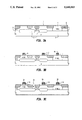
- FIG. 3A to 3F show cross-sectional views in the manufacturing sequence illustrating the method for manufacturing a Bi-CMOS semiconductor device in accordance with the present invention.
- FIG. 4 shows a cross-sectional view of the Bi-CMOS semiconductor device formed according to the manufacturing method of the present invention.
- FIG. 3A shows the process sequence from forming step of a buried layer to growing step of a gate oxide film.
- a buried layer mask is used upon the surface of a P type silicon substrate 1 in order to establish the regions for forming a bipolar transistor and a PMOS device.
- n+ buried layer 2 is formed upon the substrate 1, and an epitaxial layer 1.5 to 2 ⁇ m thick doped with phosphorus is formed.
- boron ion is implanted, diffusion is carried out at a temperature of 1180° C. for two hours, then the boron ion is diffused down to an epitaxial layer 3 and thus a p well 4 is formed up for NMOS device.
- An oxide film 5000 ⁇ thick is deposited after the removal of the remaining oxide film on it, and then a nitride film (Si 3 N 4 ) 1200 ⁇ thick is formed by a low pressure chemical vapor deposition method (LPCVD). Then active regions for respective devices are defined by means of an active region mask, and forming isolation regions of devices 5 by means of an oxide isolation method. Before the growth of the oxide film, under the isolating oxide film for the isolation of the bipolar transistors, P type junction isolation areas 6 are defined by means of a field mask and then, an impurity (such as boron) ion is implanted and diffused.
- LPCVD low pressure chemical vapor deposition method
- the N area except the P well 4 of the NMOS device is thinly ion-implanted with boron in order to control the threshold voltage of the PMOS devices, and the oxide film is removed, as well as a gate oxide film 7 of CMOS devices is grown.
- FIG. 3B shows the process of forming the emitter and collector of the bipolar transistor by means of polysilicon, and gates of the CMOS device.
- the base and the collector portions of the bipolar transistor are respectively defined by means of a mask.
- boron and phosphorous are respectively ion-implanted and diffused in order to complete the base and the collector.
- polysilicon film is deposited up to the thickness of 3000 ⁇ by means of low pressure chemical vapor deposition method, and then is ion-implanted with arsenic to form an N+ type polysilicon layer 8, as well as an oxide film 9 and a nitride film 10 are respectively deposited at the thicknesses of 2500 ⁇ and 2000 ⁇ in order to serve as a mask layer.
- gates of the NMOS and PMOS devices, and the emitter and collector of the bipolar transistors are formed by means of the reactive ion etching method, and N+ polysilicon to P+ polysilicon separation is formed by means of an anisotropic etching of oxide film and polysilicon.
- FIG. 3C shows the process of electrically insulating a side wall of the n+ type polysilicon layer 8 which serves as the emitter and collector of the bipolar transistor, and the gates of the CMOS device.
- the anisotropic etching process of a dry etching method is carried out in order to etch away all the oxide film from all the horizontal sides of the n+ type polysilicon 8 including its upper side, except the vertical side wall 11.
- FIG. 3D shows the process of etching away externally exposed portions of the epitaxial layer 3.
- the anisotropic etching process of the dry etching method is carried out in order to etch away all the nitride except a vertical side wall of the N+ type polysilicon layer 8.
- the externally exposed portions of the epitaxial layer 3 are etched away up to the thickness of 1500 ⁇ by means of the dry etching method, and then a nitride film 700 ⁇ thick is deposited upon it and etched away all the nitride except a vertical side wall of the nitride film 12 by means of the anisotropic etching process, so that only at the vertical side wall of the nitride film 12 the nitride film 13 is formed.
- FIG. 3E shows the process of depositing an oxide film in order to decrease the width of an inactive base region in the bipolar transistor, and the widths of a source/drain region in the CMOS device.
- an oxide film 14 is deposited only on the exposed portions of the epitaxial layer 3 by means of a annealing oxide growing method.
- the remaining nitride film 10, 12, and 13 serve as preventing function that the oxide film 14 is not grown into the n+ type polysilicon 15 for forming the emitter and collector of the bipolar transistor and the gate of the CMOS device.
- FIG. 3F shows the process of removing all the nitride films in order to extremely decrease the widths as mentioned above.
- portions 16 of the epitaxial layer 3 are exposed at the side walls of the n+ type polysilicon 8.
- the respective portions 16 of the epitaxial layer 3 exposed by removal of the second and third nitride film 12 and 13 have the same width as one of the laminated nitride films 12 and 13.
- the laminated nitride films 12 and 13 are formed up to the width of 3000 ⁇ .
- boron-ions of an impurity are implanted to the exposed portions 16 in which the base of the bipolar transistor and the source/drain of a PMOS device are formed, in order to make the portions p+ type.
- arsenic ions of an impurity are implanted the other exposed regions in which the source/drain of a NMOS are formed, in order to make the other exposed portions n+ type. Therefore, with annealing process, there is provided the inactive base regions of the bipolar transistor and the source/drain of the CMOS device with the extremely thin width.
- inactive base region of bipolar transistor and source/drain regions of CMOS device in a Bi-COMS are formed in proportion to the width of two nitride film at the side wall n+ type polysilicon, the widths of the base region and the source/drain region can be extremely reduced.
- the Bi-COMS according to the invention can be relatively reduced in the widths of the base region the source/drain regions of a CMOS, as compared to the prior art Bi-CMOS, junction capacitance between the base and the collector of a bipolar transistor can be reduced, junction capacitance to be produced in the source/drain of a CMOS device can be also reduced, and thus operating speed of a Bi-CMOS can be improved.
Landscapes
- Engineering & Computer Science (AREA)
- Power Engineering (AREA)
- Physics & Mathematics (AREA)
- Condensed Matter Physics & Semiconductors (AREA)
- General Physics & Mathematics (AREA)
- Computer Hardware Design (AREA)
- Microelectronics & Electronic Packaging (AREA)
- Manufacturing & Machinery (AREA)
- Metal-Oxide And Bipolar Metal-Oxide Semiconductor Integrated Circuits (AREA)
Abstract
Description
Claims (1)
Applications Claiming Priority (2)
| Application Number | Priority Date | Filing Date | Title |
|---|---|---|---|
| KR90-16866 | 1990-10-22 | ||
| KR1019900016866A KR930010116B1 (en) | 1990-10-22 | 1990-10-22 | Bicmos semiconductor device and making method of the same |
Publications (1)
| Publication Number | Publication Date |
|---|---|
| US5149663A true US5149663A (en) | 1992-09-22 |
Family
ID=19304986
Family Applications (1)
| Application Number | Title | Priority Date | Filing Date |
|---|---|---|---|
| US07/780,253 Expired - Lifetime US5149663A (en) | 1990-10-22 | 1991-10-21 | Method for manufacturing a Bi-CMOS semiconductor device |
Country Status (3)
| Country | Link |
|---|---|
| US (1) | US5149663A (en) |
| JP (1) | JPH0831543B2 (en) |
| KR (1) | KR930010116B1 (en) |
Cited By (10)
| Publication number | Priority date | Publication date | Assignee | Title |
|---|---|---|---|---|
| US5329604A (en) * | 1993-02-11 | 1994-07-12 | International Business Machines Corporation | Optical fiber coupling device and optoelectronic system utilizing same |
| GB2331845A (en) * | 1997-11-28 | 1999-06-02 | Nec Corp | Bicmos device |
| EP1030363A2 (en) * | 1999-02-18 | 2000-08-23 | Chartered Semiconductor Manufacturing Pte Ltd. | Integration of bipolar and CMOS devices for sub-0.1 micrometer transistors |
| US6117718A (en) * | 1999-08-31 | 2000-09-12 | United Microelectronics Corp. | Method for forming BJT via formulation of high voltage device in ULSI |
| US6127720A (en) * | 1997-05-19 | 2000-10-03 | Matsushita Electronics Corporation | Semiconductor device and method for manufacturing the same |
| US6313001B1 (en) | 1998-11-04 | 2001-11-06 | Telefonaktiebolaget Lm Ericsson (Publ) | Method for semiconductor manufacturing |
| US6409069B1 (en) | 1996-10-31 | 2002-06-25 | Taiyo Yuden Co., Ltd. | Apparatus for manufacturing unit elements for chip components, and chip components mounting structure |
| GB2561388A (en) * | 2017-04-13 | 2018-10-17 | Raytheon Systems Ltd | Silicon carbide integrated circuit |
| US10665703B2 (en) | 2017-04-13 | 2020-05-26 | Raytheon Systems Limited | Silicon carbide transistor |
| US10777551B2 (en) | 2016-04-15 | 2020-09-15 | Magnachip Semiconductor, Ltd. | Integrated semiconductor device and method for manufacturing the same |
Citations (2)
| Publication number | Priority date | Publication date | Assignee | Title |
|---|---|---|---|---|
| US4816423A (en) * | 1987-05-01 | 1989-03-28 | Texas Instruments Incorporated | Bicmos process for forming shallow npn emitters and mosfet source/drains |
| US5059546A (en) * | 1987-05-01 | 1991-10-22 | Texas Instruments Incorporated | BICMOS process for forming shallow NPN emitters and mosfet source/drains |
-
1990
- 1990-10-22 KR KR1019900016866A patent/KR930010116B1/en not_active IP Right Cessation
-
1991
- 1991-10-21 US US07/780,253 patent/US5149663A/en not_active Expired - Lifetime
- 1991-10-22 JP JP3273699A patent/JPH0831543B2/en not_active Expired - Lifetime
Patent Citations (2)
| Publication number | Priority date | Publication date | Assignee | Title |
|---|---|---|---|---|
| US4816423A (en) * | 1987-05-01 | 1989-03-28 | Texas Instruments Incorporated | Bicmos process for forming shallow npn emitters and mosfet source/drains |
| US5059546A (en) * | 1987-05-01 | 1991-10-22 | Texas Instruments Incorporated | BICMOS process for forming shallow NPN emitters and mosfet source/drains |
Cited By (16)
| Publication number | Priority date | Publication date | Assignee | Title |
|---|---|---|---|---|
| US5329604A (en) * | 1993-02-11 | 1994-07-12 | International Business Machines Corporation | Optical fiber coupling device and optoelectronic system utilizing same |
| US6409069B1 (en) | 1996-10-31 | 2002-06-25 | Taiyo Yuden Co., Ltd. | Apparatus for manufacturing unit elements for chip components, and chip components mounting structure |
| US6127720A (en) * | 1997-05-19 | 2000-10-03 | Matsushita Electronics Corporation | Semiconductor device and method for manufacturing the same |
| GB2331845A (en) * | 1997-11-28 | 1999-06-02 | Nec Corp | Bicmos device |
| GB2331845B (en) * | 1997-11-28 | 2000-03-29 | Nec Corp | Semiconductor device and manufacturing method for same |
| US6232638B1 (en) * | 1997-11-28 | 2001-05-15 | Nec Corporation | Semiconductor device and manufacturing method for same |
| US6313001B1 (en) | 1998-11-04 | 2001-11-06 | Telefonaktiebolaget Lm Ericsson (Publ) | Method for semiconductor manufacturing |
| EP1030363A3 (en) * | 1999-02-18 | 2004-06-16 | Chartered Semiconductor Manufacturing Pte Ltd. | Integration of bipolar and CMOS devices for sub-0.1 micrometer transistors |
| EP1030363A2 (en) * | 1999-02-18 | 2000-08-23 | Chartered Semiconductor Manufacturing Pte Ltd. | Integration of bipolar and CMOS devices for sub-0.1 micrometer transistors |
| US6117718A (en) * | 1999-08-31 | 2000-09-12 | United Microelectronics Corp. | Method for forming BJT via formulation of high voltage device in ULSI |
| US10777551B2 (en) | 2016-04-15 | 2020-09-15 | Magnachip Semiconductor, Ltd. | Integrated semiconductor device and method for manufacturing the same |
| GB2561388A (en) * | 2017-04-13 | 2018-10-17 | Raytheon Systems Ltd | Silicon carbide integrated circuit |
| GB2561388B (en) * | 2017-04-13 | 2019-11-06 | Raytheon Systems Ltd | Silicon carbide integrated circuit |
| US10665703B2 (en) | 2017-04-13 | 2020-05-26 | Raytheon Systems Limited | Silicon carbide transistor |
| US11450568B2 (en) | 2017-04-13 | 2022-09-20 | Raytheon Systems Limited | Silicon carbide integrated circuit |
| US11626325B2 (en) | 2017-04-13 | 2023-04-11 | Raytheon Systems Limited | Method of making a silicon carbide integrated circuit |
Also Published As
| Publication number | Publication date |
|---|---|
| KR930010116B1 (en) | 1993-10-14 |
| KR920008921A (en) | 1992-05-28 |
| JPH0831543B2 (en) | 1996-03-27 |
| JPH05326854A (en) | 1993-12-10 |
Similar Documents
| Publication | Publication Date | Title |
|---|---|---|
| US5489546A (en) | Method of forming CMOS devices using independent thickness spacers in a split-polysilicon DRAM process | |
| US4925805A (en) | Method of manufacturing a semiconductor device having an SOI structure using selectable etching | |
| US4824796A (en) | Process for manufacturing semiconductor BICMOS device | |
| US4318751A (en) | Self-aligned process for providing an improved high performance bipolar transistor | |
| US3983620A (en) | Self-aligned CMOS process for bulk silicon and insulating substrate device | |
| US4628589A (en) | Method for fabricating stacked CMOS structures | |
| JPH0355984B2 (en) | ||
| US5196356A (en) | Method for manufacturing BICMOS devices | |
| GB2253091A (en) | A method of producing a bipolar CMOS semiconductor device | |
| EP0135243B1 (en) | A method of producing a semiconductor structure on a substrate and a semiconductor device manufactured thereby | |
| KR940009361B1 (en) | Complicated type ic element | |
| US5149663A (en) | Method for manufacturing a Bi-CMOS semiconductor device | |
| US4954456A (en) | Fabrication method for high speed and high packing density semiconductor device (BiCMOS) | |
| JPH0669431A (en) | Method for manufacture of bipolar transistor and cmos transistor on soi substrate and these transistors | |
| US5731240A (en) | Manufacturing method for semiconductor depositing device | |
| US6445043B1 (en) | Isolated regions in an integrated circuit | |
| US5115296A (en) | Preferential oxidization self-aligned contact technology | |
| US5158900A (en) | Method of separately fabricating a base/emitter structure of a BiCMOS device | |
| KR910000020B1 (en) | Manufacture of semiconductor device | |
| US5606192A (en) | Semiconductor integrated circuits having bipolar transistors and LDD-structured MOSFET | |
| KR100408000B1 (en) | Method for Forming Semiconductor Device | |
| JPS60241261A (en) | Semiconductor device and manufacture thereof | |
| JPH0729971A (en) | Manufacture of semiconductor device | |
| US4047285A (en) | Self-aligned CMOS for bulk silicon and insulating substrate device | |
| KR950010878B1 (en) | Bipolar transistor manufacturing process |
Legal Events
| Date | Code | Title | Description |
|---|---|---|---|
| AS | Assignment |
Owner name: KOREA ELECTRONICS AND TELECOMMUNICATIONS RESEARACH Free format text: ASSIGNMENT OF ASSIGNORS INTEREST.;ASSIGNOR:CHAI, SANG H.;REEL/FRAME:005926/0677 Effective date: 19911023 |
|
| STCF | Information on status: patent grant |
Free format text: PATENTED CASE |
|
| FEPP | Fee payment procedure |
Free format text: PAYOR NUMBER ASSIGNED (ORIGINAL EVENT CODE: ASPN); ENTITY STATUS OF PATENT OWNER: SMALL ENTITY |
|
| REFU | Refund |
Free format text: REFUND PROCESSED. MAINTENANCE FEE HAS ALREADY BEEN PAID (ORIGINAL EVENT CODE: R160); ENTITY STATUS OF PATENT OWNER: SMALL ENTITY |
|
| FPAY | Fee payment |
Year of fee payment: 4 |
|
| FPAY | Fee payment |
Year of fee payment: 8 |
|
| FPAY | Fee payment |
Year of fee payment: 12 |
|
| FEPP | Fee payment procedure |
Free format text: PAYER NUMBER DE-ASSIGNED (ORIGINAL EVENT CODE: RMPN); ENTITY STATUS OF PATENT OWNER: SMALL ENTITY Free format text: PAYOR NUMBER ASSIGNED (ORIGINAL EVENT CODE: ASPN); ENTITY STATUS OF PATENT OWNER: SMALL ENTITY |
|
| FEPP | Fee payment procedure |
Free format text: PAYER NUMBER DE-ASSIGNED (ORIGINAL EVENT CODE: RMPN); ENTITY STATUS OF PATENT OWNER: SMALL ENTITY Free format text: PAYOR NUMBER ASSIGNED (ORIGINAL EVENT CODE: ASPN); ENTITY STATUS OF PATENT OWNER: SMALL ENTITY |