US5148246A - Cell array of a non-volatile semiconductor memory devices - Google Patents
Cell array of a non-volatile semiconductor memory devices Download PDFInfo
- Publication number
- US5148246A US5148246A US07/704,048 US70404891A US5148246A US 5148246 A US5148246 A US 5148246A US 70404891 A US70404891 A US 70404891A US 5148246 A US5148246 A US 5148246A
- Authority
- US
- United States
- Prior art keywords
- gate electrodes
- insulating film
- floating gate
- active regions
- portions
- Prior art date
- Legal status (The legal status is an assumption and is not a legal conclusion. Google has not performed a legal analysis and makes no representation as to the accuracy of the status listed.)
- Expired - Lifetime
Links
Images


Classifications
-
- H—ELECTRICITY
- H10—SEMICONDUCTOR DEVICES; ELECTRIC SOLID-STATE DEVICES NOT OTHERWISE PROVIDED FOR
- H10B—ELECTRONIC MEMORY DEVICES
- H10B69/00—Erasable-and-programmable ROM [EPROM] devices not provided for in groups H10B41/00 - H10B63/00, e.g. ultraviolet erasable-and-programmable ROM [UVEPROM] devices
-
- H—ELECTRICITY
- H10—SEMICONDUCTOR DEVICES; ELECTRIC SOLID-STATE DEVICES NOT OTHERWISE PROVIDED FOR
- H10B—ELECTRONIC MEMORY DEVICES
- H10B41/00—Electrically erasable-and-programmable ROM [EEPROM] devices comprising floating gates
- H10B41/30—Electrically erasable-and-programmable ROM [EEPROM] devices comprising floating gates characterised by the memory core region
Definitions
- the present invention generally relates to non-volatile semiconductor memory devices, and more particularly to a cell array of such devices wherein each device comprises an erasable and programmable read only memory device having a floating gate and a control gate.
- FIG. 1 shows a conventional erasable and programmable read only memory (EPROM) disclosed in U.S. Pat. No. 4,893,705 or Japanese Laid-Open Patent Publication No. 56-130975 (which corresponds to U.S. patent application Ser. No. 88,789 filed on Oct. 29, 1979).
- Active regions of a plurality of EPROM cells T11, T12, T21 and T22 are electrically coupled through a bulk interconnection line.
- the EPROM cells T11, T12, T21 and T22 are arranged as follows.
- Selective oxide films (field insulation (oxidation) films) 1b having rectangular plans are formed on a top surface of a semiconductor substrate 1a and spaced apart from each other so that the field insulation films 1b are arranged in a matrix.
- Regions surrounded by the field insulation films 1b are arranged in a grid and serve as element formation regions 1c.
- Floating gate electrodes 1e are formed at a center part of belt-shaped portions 1d.
- An insulating film is formed on the entire surface including the floating gate electrodes 1e, and control gate electrodes 1f are formed on the insulating film so that the control gate electrodes 1f overlap with the floating gate electrodes 1e.
- Active regions 1g are formed on both sides of the gate electrodes 1e and 1f by a self-alignment process.
- the active regions 1g are integrally formed in X-shaped regions of the element formation regions 1c so that the EPROM cells T11, T12, T21 and T22 are coupled.
- the control gate electrodes 1f are formed at an angle of about 45° with respect to the direction in which the belt-shaped portions 1d run, and arranged so that the control gate electrodes 1f run above the floating gate electrodes 1e.
- the floating gate electrodes 1e and the control gate electrodes 1f have belt-shaped portions so that they are orthogonal to the belt-shaped portions 1d.
- An interlayer insulating film (not shown) is formed on the control gate electrodes 1f.
- Contact holes 1h are formed at positions of the interlayer insulating film which correspond to the center portions of the X-shaped portions of the active regions 1g.
- Bit lines BL which are formed on the interlayer insulating film, are formed so that the bit lines BL are electrically in contact with the active regions 1g through the contact holes 1h.
- a device including the EPROM cells T11, T12, T21 and T22 has an equivalent circuit shown in FIG. 2.
- a signal is applied to the control gate electrode 1f of the cell T22 via a word line WL2, and signals are applied to the two active regions 1g through bit lines BL2 and BL3.
- the floating gate electrodes 1e and the control gate electrodes 1f are formed as follows. Referring to FIG. 3A, a first polysilicon film 1i provided for forming the floating gate electrodes 1e is formed on the entire surface. Next, the first polysilicon film 1i is patterned so that patterned portions run parallel to the bit lines BL, that is, the patterned portions are inclined at approximately 45° with respect to the long-side directions of the belt-shaped portions 1d in which the long-side edges thereof run.
- a second polysilicon film 1j provided for forming the control gate electrodes 1f, is formed on the entire surface including the interlayer insulating film.
- the first and second polysilicon films 1i and 1j are patterned. Thereby, the floating gate electrodes 1e and the control gate electrodes 1f are formed so that they have no positional error in the width direction thereof.
- the ends of the floating gate electrodes 1e are close to the belt-shaped portions 1d of the element formation regions 1c. If a patterning error occurs during the step in which the first polysilicon film 1i is patterned, as shown in FIG. 4A, one of the two ends of the floating gate electrode 1e is positioned above the belt-shaped portion 1d and the floating gate electrode 1f is positioned above the belt-shaped portion 1d. Thus, as shown in FIG. 4B, the control gate electrode 1f has a portion which does not overlap with the floating gate electrode 1e.
- the threshold voltage of the EPROM cell transistor varies due to the existence/non-existence of a charge stored in the floating gate electrode 1e of the transistor.
- This variation in the threshold voltage is used for storing information. For example, when the floating gate electrode 1e is electrified so that it has a negative polarity, a channel is not formed in the semiconductor substrate 1a even if a predetermined voltage is applied to the control gate electrode 1f. Thus, no current passes between the active regions 1a located on both sides of the floating gate electrode 1e, so that the transistor is maintained in the OFF state. In this way, data is written into the EPROM cell.
- the floating gate electrode 1e when the floating gate electrode 1e is not electrified, the electric field caused by applying a voltage to the control gate electrode 1f is not reduced by the floating gate electrode 1e. Thus, a channel is formed under the floating gate electrode 1e, so that a current passes between the active regions 1g located on both sides of the floating gate electrode 1e. In this way, no data is written into the EPROM cell.
- control gate electrode 1f positionally deviates from the floating gate electrode 1d with respect to the belt-shaped portion 1d
- the electric field formed by the control gate electrode 1f directly affects the semiconductor substrate 1a.
- the above-mentioned positional deviation of the floating gate electrode 1e forms a portion which cannot prevent the formation of the channel. This increases errors in readout data.
- a more specific object of the present invention is to provide a cell array in which data can be definitely read even if a positional error, caused at the step where the floating gate electrodes are formed, occurs.
- a cell array of non-volatile memory semiconductor memory devices comprising: a semiconductor substrate having a first conduction type; a first insulating film formed on the semiconductor substrate; a plurality of active regions formed in the semiconductor substrate, each of the active regions having a second conduction type opposite to the first conduction type; a plurality of floating gate electrodes formed on the first insulating film; a second insulating film covering the floating gate electrodes; a plurality of control gate electrodes which are formed on the second insulating film and which run above the floating gate electrodes; and bit lines electrically coupled to the active regions, each of the active regions having a substantially H-shaped surface portion close to four adjacent floating gate electrodes.
- FIG. 1 is a plan view of a conventional array of EPROM cells
- FIG. 2 is a circuit diagram of a conventional EPROM device having the array shown in FIG. 1;
- FIGS. 3A, 3B and 3C are diagrams illustrating a process of producing the array shown in FIG. 1;
- FIGS. 4A and 4B are diagrams illustrating a disadvantage of the conventional array shown in FIG. 1;
- FIG. 5 is a plan view of an array of EPROM cells according to a first preferred embodiment of the present invention.
- FIG. 6A is a cross-sectional view taken along line VI A --VI A shown in FIG. 5;
- FIG. 6B is a cross-sectional view taken along line VI B --VI B shown in FIG. 5;
- FIGS. 7A, 7B and 7C are diagrams showing a process of producing the array shown in FIG. 5;
- FIGS. 8A and 8B are diagrams showing an advantage of the first embodiment of the present invention shown in FIG. 5;
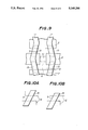
- FIG. 9 is a plan view of an array according to a second preferred embodiment of the present invention.
- FIGS. 10A and 10B are diagrams showing an advantage of the array shown in FIG. 9.
- FIGS. 5, 6A and 6B A description will now be given of a cell array according to a first preferred embodiment of the present invention with reference to FIGS. 5, 6A and 6B.
- the cell array comprises a silicon semiconductor substrate 1 having a predetermined conduction type.
- a plurality of selective oxide films (field insulation films) 2 are formed on a top surface of the silicon substrate 1, and long-side edges of the field insulation films 2 run in an identical direction.
- the field insulation films 2 are spaced apart from each other at a definite distance and alternately arranged.
- Floating gate electrodes 5 are formed on the thermal oxidation films 4 on the element formation regions 3 and the floating gate electrodes 5 structurally interconnect the adjacent field insulation films 2. As shown in FIG. 6B, the opposite end portions of each of the floating gate electrodes 5 lie respective, two adjacent field insulation films 2. Each of the floating gate electrodes 5 has two opposite ends parallel to the direction in which the long-side edges of the field insulation films 2 run. In addition, the opposite ends of the floating gate electrodes 5, arranged in the direction in which the long-side edges of the field insulation films 2 run, are located on identical imaginary lines.
- an insulating film 6 formed of SiO 2 is formed on the floating gate electrodes 5.
- Control gate electrodes 7 are formed on the SiO 2 film 6. Each of the control gate electrodes 7 is arranged so that it crosses the long-side edges of the field insulation films 2 and runs above some of the floating gate electrodes 5. Each of the control gate electrodes 7 has a width which is substantially identical to that of each of the floating gate electrodes 5.
- the control gate electrodes 7 are made of, for example, doped polysilicon.
- the floating gate electrodes 5 and the control gate electrodes 7 are positioned so that they are spaced apart from the short-side edges of the field insulation films 2 at a distance large enough to obtain smooth step portions (in other words, they are located at positions close to the center portions of the thermal oxidation films 4).
- the floating gate electrodes 5 and the control gate electrodes 7 are obliquely arranged at an angle of approximately 45° with respect to the long-side edges of the field insulation films 2 so that they obliquely cross the element formation regions 3.
- Active regions 8, which have a conduction type opposite to that of the silicon substrate 1, are formed by a self-alignment process in which impurities are introduced into the element formation regions 3 on both sides of each of the floating gate electrodes 5.
- Each of the active regions 8 is integrally formed along the long-side and short-side edges of the field insulation films 2 and extends up to the side-end portions of the other floating gate electrodes 5.
- Each of the active regions 8 has a substantially H-shaped surface portion illustrated by a thick solid line shown in FIG. 5.
- Channel formation regions are formed in portions of the silicon substrate 1 which are located under the floating gate electrodes 5 and which are sandwiched between the neighboring active regions 8.
- An EPROM cell T is formed by the portion of the silicon substrate 1 in the element formation region 3, the floating gate electrode 5, the control gate electrode 7 and the respective active regions 8 located on the opposite sides of these electrodes.
- an insulating film 9 formed of, for example, SiO 2 is formed on the entire surface.
- Bit lines BL are formed on the SiO 2 film 9 so that they run parallel to the long-side edges of the field insulation films 2. The bit lines BL are electrically in contact with the center portion of the H-shaped active regions 8 through the contact holes 10.
- the first embodiment of the present invention has the same equivalent circuit as the conventional device shown in FIG. 2.
- a voltage is applied to the control gate electrode 7 via the corresponding word line WL, and a voltage is applied across the active regions 8 via the neighboring two bit lines BL, so that a desired EPROM cell T is selected.
- a channel is generated in the portion of the silicon substrate 1 under the floating gate electrode 5, so that the carrier is allowed to move.
- a current passes through the bit line BL, so that it can be recognized that no information is stored in the selected EPROM cell T.
- no charge is stored in the floating gate electrode 5
- no channel is generated and no current passes through the bit line BL, so that information has been written into the selected EPROM cell T.
- the field insulation films 2 formed of SiO 2 are formed to a thickness equal to, for example, 5000 angstroms by a LOCOS process.
- a polysilicon film for forming the floating gate electrodes 5 is deposited to a thickness of, for example, 1000 angstroms on the SiO 2 film 4 by a CVD process.
- POCl 3 is thermally diffused into the polysilicon film at 850° C. After that, as shown in FIG.
- the polysilicon film is patterned into films 5a running parallel to the long-side edges of the field insulation films 2 by a conventional photolithography technique and an RIE etching in which a gas of CCl 4 /O 2 is used. Then, the SiO 2 film 6 is thermally formed to a thickness of, for example, 250 angstroms. Then, as shown in FIG. 7B, a polysilicon film 7a, used for forming the control gate electrodes 7, is deposited to a thickness equal to, for example, 2000 angstroms by a CVD process. POCl 3 is thermally diffused into the polysilicon film at 850° C.
- the polysilicon films 5a and 7a are patterned into a belt shape at the same time, so that the floating gate electrodes 5 and the control gate electrodes 7 are defined.
- the SiO 2 film 9 is formed to a thickness of, for example, 200 agnstroms on the surface of the control gate electrodes 7 by a thermal oxidation process.
- + ions are introduced at 4 ⁇ 10 15 /cm 2 at 70 keV, and an insulating film is formed by a CVD process. It is preferable to form a BPSG (boron phosphosilicate glass) film to a thickness of, for example, 5000 angstroms, on the entire surface.
- the BPSG film is subjected to a reflow process in order to flatten the surface thereof.
- the contact holes 10 are formed in the BPSG film, the SiO 2 film 9, and the SiO 2 film 4 by the photolithography technique and RIE process in which a gas of CHF 3 /He is used. After that, A1 bit lines are formed.
- each field insulation film 2 has a substantially rectangular planar area in place of the square planar area of the prior art devices.
- the floating gate electrodes 5 and the control gate electrodes 7 run on the thermal oxidation films 4 in the direction perpendicular to the direction in which the long-side edges of the thermal oxidation films 4 extend, and obliquely cross the element formation regions 3.
- the floating gate electrodes 5 and the control gate electrodes 7 have bent portions in the vicinity of the element formation regions 3.
- the adjacent control gate electrodes 17 are spaced apart from each other, alternately, at a maximum or a minimum distance at successive respective bent portions thereof.
- control gate electrodes 17 have alternate, "less-than” symbol, “greater-than” symbol-shaped surface portions on the field insulation films 2.
- Floating gate electrodes 15 beneath the control gate electrodes 17 have a substantially parallelogram planar surface shape. That is, the two opposite short-side ends of each of the floating gate electrodes 15 run in parallel to the long-side edges of the field insulation films 2, and the two opposite long-side ends thereof run parallel to each other. It should be noted that the area of each floating gate electrode 15 on the element formation region 3 does not change even if the floating gate electrode 15 has any positional error, as shown in FIG. 10A or 10B. Thus, the readout potential and write potential are not affected by such a positional error. That is, a potential V FG of the floating gate electrode 15 is defined as follows:
- C1 is the coupling capacitance between the floating gate electrode 15 and the control gate electrode 7
- C2 is the coupling capacitance between the floating gate electrode 15 and the semiconductor substrate 1
- Q is a charge stored in the floating gate electrode 15
- V CF is a voltage applied to the control gate electrode 17
Landscapes
- Non-Volatile Memory (AREA)
- Semiconductor Memories (AREA)
Abstract
Description
V.sub.FG =K(V.sub.CF +Q/C1)
Claims (23)
Applications Claiming Priority (2)
| Application Number | Priority Date | Filing Date | Title |
|---|---|---|---|
| JP2131713A JP3032240B2 (en) | 1990-05-22 | 1990-05-22 | Semiconductor storage device |
| JP2-131713 | 1990-05-22 |
Publications (1)
| Publication Number | Publication Date |
|---|---|
| US5148246A true US5148246A (en) | 1992-09-15 |
Family
ID=15064460
Family Applications (1)
| Application Number | Title | Priority Date | Filing Date |
|---|---|---|---|
| US07/704,048 Expired - Lifetime US5148246A (en) | 1990-05-22 | 1991-05-22 | Cell array of a non-volatile semiconductor memory devices |
Country Status (5)
| Country | Link |
|---|---|
| US (1) | US5148246A (en) |
| EP (1) | EP0458238B1 (en) |
| JP (1) | JP3032240B2 (en) |
| KR (1) | KR950008387B1 (en) |
| DE (1) | DE69132402T2 (en) |
Cited By (3)
| Publication number | Priority date | Publication date | Assignee | Title |
|---|---|---|---|---|
| US20040041199A1 (en) * | 2002-08-28 | 2004-03-04 | Tower Semiconductor Ltd. | Non-volatile memory transistor array implementing "h" shaped source/drain regions and method for fabricating same |
| US20100329012A1 (en) * | 2009-06-30 | 2010-12-30 | Kabushiki Kaisha Toshiba | Semiconductor memory device |
| US20130320451A1 (en) * | 2012-06-01 | 2013-12-05 | Taiwan Semiconductor Manufacturing Company, Ltd., ("Tsmc") | Semiconductor device having non-orthogonal element |
Families Citing this family (6)
| Publication number | Priority date | Publication date | Assignee | Title |
|---|---|---|---|---|
| JP2748885B2 (en) * | 1995-03-06 | 1998-05-13 | 日本電気株式会社 | Semiconductor integrated circuit device |
| KR970051170A (en) * | 1995-12-29 | 1997-07-29 | 김주용 | Memory cell array and program method using the same |
| KR19980014258A (en) * | 1996-08-09 | 1998-05-25 | 김주용 | The memory cell array |
| KR100246782B1 (en) * | 1996-08-30 | 2000-03-15 | 김영환 | The memory cell array |
| KR100277888B1 (en) * | 1997-12-31 | 2001-02-01 | 김영환 | Flash memory and method for fabricating the same |
| JP5204159B2 (en) * | 2003-11-14 | 2013-06-05 | ラピスセミコンダクタ株式会社 | Manufacturing method of semiconductor memory device |
Citations (3)
| Publication number | Priority date | Publication date | Assignee | Title |
|---|---|---|---|---|
| JPS56130975A (en) * | 1979-10-29 | 1981-10-14 | Texas Instruments Inc | Semiconductor memory device |
| US4839705A (en) * | 1987-12-16 | 1989-06-13 | Texas Instruments Incorporated | X-cell EEPROM array |
| US4935791A (en) * | 1988-01-12 | 1990-06-19 | Oki Electric Industry Co., Ltd. | Nonvolatile semiconductor memory device of shared contact scheme not having inclined wiring |
Family Cites Families (3)
| Publication number | Priority date | Publication date | Assignee | Title |
|---|---|---|---|---|
| JPH01108778A (en) * | 1987-10-21 | 1989-04-26 | Mitsubishi Electric Corp | Semiconductor storage device |
| US5095344A (en) * | 1988-06-08 | 1992-03-10 | Eliyahou Harari | Highly compact eprom and flash eeprom devices |
| FR2638285B1 (en) * | 1988-10-25 | 1992-06-19 | Commissariat Energie Atomique | HIGH INTEGRATION DENSITY INTEGRATED CIRCUIT SUCH AS EPROM AND CORRESPONDING METHOD |
-
1990
- 1990-05-22 JP JP2131713A patent/JP3032240B2/en not_active Expired - Fee Related
-
1991
- 1991-05-21 EP EP91108131A patent/EP0458238B1/en not_active Expired - Lifetime
- 1991-05-21 DE DE69132402T patent/DE69132402T2/en not_active Expired - Fee Related
- 1991-05-22 US US07/704,048 patent/US5148246A/en not_active Expired - Lifetime
- 1991-05-22 KR KR1019910008235A patent/KR950008387B1/en not_active Expired - Fee Related
Patent Citations (3)
| Publication number | Priority date | Publication date | Assignee | Title |
|---|---|---|---|---|
| JPS56130975A (en) * | 1979-10-29 | 1981-10-14 | Texas Instruments Inc | Semiconductor memory device |
| US4839705A (en) * | 1987-12-16 | 1989-06-13 | Texas Instruments Incorporated | X-cell EEPROM array |
| US4935791A (en) * | 1988-01-12 | 1990-06-19 | Oki Electric Industry Co., Ltd. | Nonvolatile semiconductor memory device of shared contact scheme not having inclined wiring |
Cited By (7)
| Publication number | Priority date | Publication date | Assignee | Title |
|---|---|---|---|---|
| US20040041199A1 (en) * | 2002-08-28 | 2004-03-04 | Tower Semiconductor Ltd. | Non-volatile memory transistor array implementing "h" shaped source/drain regions and method for fabricating same |
| US6765259B2 (en) * | 2002-08-28 | 2004-07-20 | Tower Semiconductor Ltd. | Non-volatile memory transistor array implementing “H” shaped source/drain regions and method for fabricating same |
| US20100329012A1 (en) * | 2009-06-30 | 2010-12-30 | Kabushiki Kaisha Toshiba | Semiconductor memory device |
| US8189360B2 (en) * | 2009-06-30 | 2012-05-29 | Kabushiki Kaisha Toshiba | Semiconductor memory device |
| US20130320451A1 (en) * | 2012-06-01 | 2013-12-05 | Taiwan Semiconductor Manufacturing Company, Ltd., ("Tsmc") | Semiconductor device having non-orthogonal element |
| US10276488B2 (en) | 2012-06-01 | 2019-04-30 | Taiwan Semiconductor Manufacturing Company, Ltd. | Method of fabricating field effect transistor having non-orthogonal gate electrode |
| US11211323B2 (en) | 2012-06-01 | 2021-12-28 | Taiwan Semiconductor Manufacturing Company, Ltd. | Method of fabricating field effect transistor having non-orthogonal gate electrode |
Also Published As
| Publication number | Publication date |
|---|---|
| EP0458238A3 (en) | 1992-04-08 |
| JP3032240B2 (en) | 2000-04-10 |
| EP0458238A2 (en) | 1991-11-27 |
| DE69132402D1 (en) | 2000-10-12 |
| KR950008387B1 (en) | 1995-07-28 |
| DE69132402T2 (en) | 2001-04-05 |
| KR910020885A (en) | 1991-12-20 |
| JPH0426157A (en) | 1992-01-29 |
| EP0458238B1 (en) | 2000-09-06 |
Similar Documents
| Publication | Publication Date | Title |
|---|---|---|
| US6151249A (en) | NAND-type EEPROM having bit lines and source lines commonly coupled through enhancement and depletion transistors | |
| US5392237A (en) | Semiconductor memory device with EEPROM in trench with polysilicon/metal contacting to source and drain in virtual ground type array | |
| US5053840A (en) | Semiconductor device having a gate electrode consisting of a plurality of layers | |
| US5300799A (en) | Nonvolatile semiconductor storage device with ferroelectric capacitors | |
| JP3366173B2 (en) | Manufacturing method of nonvolatile semiconductor memory | |
| US5492846A (en) | Fabrication method of nonvolatile semiconductor memory device | |
| US6255170B1 (en) | Flash memory and method for fabricating the same | |
| US5148246A (en) | Cell array of a non-volatile semiconductor memory devices | |
| JP3441140B2 (en) | Semiconductor storage device | |
| JP3465397B2 (en) | Semiconductor nonvolatile memory device | |
| JP3049100B2 (en) | Semiconductor device and manufacturing method thereof | |
| US6335553B1 (en) | Nonvolatile semiconductor memory and method of fabrication | |
| US20030008488A1 (en) | Method for manufacturing non-volatile semiconductor memory and non-volatile semiconductor memory manufactured thereby | |
| KR930006142B1 (en) | Mos semiconductor device with inversion layer | |
| US5153684A (en) | Nonvolatile semiconductor memory device with offset transistor | |
| JPH0745797A (en) | Semiconductor memory device | |
| EP1039536A1 (en) | Ferroelectric memory or a method of producing the same | |
| JPH0334578A (en) | Nonvolatile semiconductor storage device and manufacture thereof | |
| US5210048A (en) | Nonvolatile semiconductor memory device with offset transistor and method for manufacturing the same | |
| JP3400231B2 (en) | Semiconductor storage device and manufacturing method | |
| JPS62136880A (en) | Semiconductor memory device and manufacture of the same | |
| JPH0334579A (en) | Nonvolatile semiconductor storage device and manufacture thereof | |
| JPH0414265A (en) | Semiconductor storage device and its manufacture | |
| JPH09116031A (en) | Nonvolatile semiconductor storage device and its manufacturing method | |
| JPH06260618A (en) | Nonvolatile semiconductor storage |
Legal Events
| Date | Code | Title | Description |
|---|---|---|---|
| AS | Assignment |
Owner name: FUJITSU LIMITED, JAPAN Free format text: ASSIGNMENT OF ASSIGNORS INTEREST.;ASSIGNOR:EMA, TAIJI;REEL/FRAME:005714/0884 Effective date: 19910510 |
|
| STCF | Information on status: patent grant |
Free format text: PATENTED CASE |
|
| FEPP | Fee payment procedure |
Free format text: PAYOR NUMBER ASSIGNED (ORIGINAL EVENT CODE: ASPN); ENTITY STATUS OF PATENT OWNER: LARGE ENTITY |
|
| CC | Certificate of correction | ||
| FPAY | Fee payment |
Year of fee payment: 4 |
|
| FPAY | Fee payment |
Year of fee payment: 8 |
|
| FPAY | Fee payment |
Year of fee payment: 12 |
|
| AS | Assignment |
Owner name: FUJITSU MICROELECTRONICS LIMITED, JAPAN Free format text: ASSIGNMENT OF ASSIGNORS INTEREST;ASSIGNOR:FUJITSU LIMITED;REEL/FRAME:021985/0715 Effective date: 20081104 Owner name: FUJITSU MICROELECTRONICS LIMITED,JAPAN Free format text: ASSIGNMENT OF ASSIGNORS INTEREST;ASSIGNOR:FUJITSU LIMITED;REEL/FRAME:021985/0715 Effective date: 20081104 |
|
| AS | Assignment |
Owner name: FUJITSU SEMICONDUCTOR LIMITED, JAPAN Free format text: CHANGE OF NAME;ASSIGNOR:FUJITSU MICROELECTRONICS LIMITED;REEL/FRAME:024794/0500 Effective date: 20100401 |