US5129727A - Liquid crystal device having the orientation control films which comprise a fluorine-containing aliphatic or alicyclic polyimide and display apparatus - Google Patents
Liquid crystal device having the orientation control films which comprise a fluorine-containing aliphatic or alicyclic polyimide and display apparatus Download PDFInfo
- Publication number
- US5129727A US5129727A US07/676,519 US67651991A US5129727A US 5129727 A US5129727 A US 5129727A US 67651991 A US67651991 A US 67651991A US 5129727 A US5129727 A US 5129727A
- Authority
- US
- United States
- Prior art keywords
- liquid crystal
- fluorine
- crystal device
- polyimide
- aliphatic
- Prior art date
- Legal status (The legal status is an assumption and is not a legal conclusion. Google has not performed a legal analysis and makes no representation as to the accuracy of the status listed.)
- Expired - Fee Related
Links
- 229910052731 fluorine Inorganic materials 0.000 title claims abstract description 53
- 239000011737 fluorine Substances 0.000 title claims abstract description 53
- 229920001721 polyimide Polymers 0.000 title claims abstract description 49
- YCKRFDGAMUMZLT-UHFFFAOYSA-N Fluorine atom Chemical compound [F] YCKRFDGAMUMZLT-UHFFFAOYSA-N 0.000 title claims abstract description 39
- 239000004642 Polyimide Substances 0.000 title claims abstract description 34
- 125000001931 aliphatic group Chemical group 0.000 title claims abstract description 34
- 125000002723 alicyclic group Chemical group 0.000 title claims abstract description 15
- 239000004973 liquid crystal related substance Substances 0.000 title claims description 121
- 239000005262 ferroelectric liquid crystals (FLCs) Substances 0.000 claims abstract description 24
- 239000000758 substrate Substances 0.000 claims abstract description 24
- 125000003118 aryl group Chemical group 0.000 claims description 13
- 238000011282 treatment Methods 0.000 claims description 6
- 125000001153 fluoro group Chemical group F* 0.000 claims 14
- 101100434170 Oryza sativa subsp. japonica ACR2.1 gene Proteins 0.000 claims 1
- 101100434171 Oryza sativa subsp. japonica ACR2.2 gene Proteins 0.000 claims 1
- 230000005684 electric field Effects 0.000 description 26
- 239000010408 film Substances 0.000 description 20
- 239000004990 Smectic liquid crystal Substances 0.000 description 19
- 230000003287 optical effect Effects 0.000 description 19
- 210000002858 crystal cell Anatomy 0.000 description 17
- 230000004044 response Effects 0.000 description 16
- 238000000034 method Methods 0.000 description 12
- 206010047571 Visual impairment Diseases 0.000 description 10
- 239000004952 Polyamide Substances 0.000 description 8
- 239000002253 acid Substances 0.000 description 8
- 150000004985 diamines Chemical class 0.000 description 8
- 229920002647 polyamide Polymers 0.000 description 8
- 239000000243 solution Substances 0.000 description 8
- 239000007921 spray Substances 0.000 description 7
- 239000000463 material Substances 0.000 description 6
- 238000002834 transmittance Methods 0.000 description 6
- 150000001244 carboxylic acid anhydrides Chemical class 0.000 description 5
- 230000008859 change Effects 0.000 description 5
- 239000011521 glass Substances 0.000 description 5
- 230000010287 polarization Effects 0.000 description 5
- 230000002269 spontaneous effect Effects 0.000 description 5
- -1 4-aminophenoxy Chemical group 0.000 description 4
- VYPSYNLAJGMNEJ-UHFFFAOYSA-N Silicium dioxide Chemical compound O=[Si]=O VYPSYNLAJGMNEJ-UHFFFAOYSA-N 0.000 description 4
- 210000004027 cell Anatomy 0.000 description 4
- 230000003098 cholesteric effect Effects 0.000 description 4
- 230000000052 comparative effect Effects 0.000 description 4
- KZTYYGOKRVBIMI-UHFFFAOYSA-N diphenyl sulfone Chemical compound C=1C=CC=CC=1S(=O)(=O)C1=CC=CC=C1 KZTYYGOKRVBIMI-UHFFFAOYSA-N 0.000 description 4
- 238000009826 distribution Methods 0.000 description 4
- ZMXDDKWLCZADIW-UHFFFAOYSA-N N,N-Dimethylformamide Chemical compound CN(C)C=O ZMXDDKWLCZADIW-UHFFFAOYSA-N 0.000 description 3
- 239000011324 bead Substances 0.000 description 3
- 230000008569 process Effects 0.000 description 3
- 239000002966 varnish Substances 0.000 description 3
- YBRVSVVVWCFQMG-UHFFFAOYSA-N 4,4'-diaminodiphenylmethane Chemical compound C1=CC(N)=CC=C1CC1=CC=C(N)C=C1 YBRVSVVVWCFQMG-UHFFFAOYSA-N 0.000 description 2
- IAZDPXIOMUYVGZ-UHFFFAOYSA-N Dimethylsulphoxide Chemical compound CS(C)=O IAZDPXIOMUYVGZ-UHFFFAOYSA-N 0.000 description 2
- SECXISVLQFMRJM-UHFFFAOYSA-N N-Methylpyrrolidone Chemical compound CN1CCCC1=O SECXISVLQFMRJM-UHFFFAOYSA-N 0.000 description 2
- GWEVSGVZZGPLCZ-UHFFFAOYSA-N Titan oxide Chemical compound O=[Ti]=O GWEVSGVZZGPLCZ-UHFFFAOYSA-N 0.000 description 2
- PNEYBMLMFCGWSK-UHFFFAOYSA-N aluminium oxide Inorganic materials [O-2].[O-2].[O-2].[Al+3].[Al+3] PNEYBMLMFCGWSK-UHFFFAOYSA-N 0.000 description 2
- 230000015572 biosynthetic process Effects 0.000 description 2
- 150000001732 carboxylic acid derivatives Chemical class 0.000 description 2
- 238000000576 coating method Methods 0.000 description 2
- 150000001875 compounds Chemical class 0.000 description 2
- ZUOUZKKEUPVFJK-UHFFFAOYSA-N diphenyl Chemical compound C1=CC=CC=C1C1=CC=CC=C1 ZUOUZKKEUPVFJK-UHFFFAOYSA-N 0.000 description 2
- 239000004744 fabric Substances 0.000 description 2
- 238000010438 heat treatment Methods 0.000 description 2
- 125000001997 phenyl group Chemical group [H]C1=C([H])C([H])=C(*)C([H])=C1[H] 0.000 description 2
- 239000002243 precursor Substances 0.000 description 2
- 239000000377 silicon dioxide Substances 0.000 description 2
- WZCQRUWWHSTZEM-UHFFFAOYSA-N 1,3-phenylenediamine Chemical compound NC1=CC=CC(N)=C1 WZCQRUWWHSTZEM-UHFFFAOYSA-N 0.000 description 1
- CBCKQZAAMUWICA-UHFFFAOYSA-N 1,4-phenylenediamine Chemical compound NC1=CC=C(N)C=C1 CBCKQZAAMUWICA-UHFFFAOYSA-N 0.000 description 1
- POAOYUHQDCAZBD-UHFFFAOYSA-N 2-butoxyethanol Chemical compound CCCCOCCO POAOYUHQDCAZBD-UHFFFAOYSA-N 0.000 description 1
- MFTFTIALAXXIMU-UHFFFAOYSA-N 3-[4-[2-[4-(3-aminophenoxy)phenyl]-1,1,1,3,3,3-hexafluoropropan-2-yl]phenoxy]aniline Chemical compound NC1=CC=CC(OC=2C=CC(=CC=2)C(C=2C=CC(OC=3C=C(N)C=CC=3)=CC=2)(C(F)(F)F)C(F)(F)F)=C1 MFTFTIALAXXIMU-UHFFFAOYSA-N 0.000 description 1
- WECDUOXQLAIPQW-UHFFFAOYSA-N 4,4'-Methylene bis(2-methylaniline) Chemical compound C1=C(N)C(C)=CC(CC=2C=C(C)C(N)=CC=2)=C1 WECDUOXQLAIPQW-UHFFFAOYSA-N 0.000 description 1
- ICNFHJVPAJKPHW-UHFFFAOYSA-N 4,4'-Thiodianiline Chemical compound C1=CC(N)=CC=C1SC1=CC=C(N)C=C1 ICNFHJVPAJKPHW-UHFFFAOYSA-N 0.000 description 1
- UITKHKNFVCYWNG-UHFFFAOYSA-N 4-(3,4-dicarboxybenzoyl)phthalic acid Chemical compound C1=C(C(O)=O)C(C(=O)O)=CC=C1C(=O)C1=CC=C(C(O)=O)C(C(O)=O)=C1 UITKHKNFVCYWNG-UHFFFAOYSA-N 0.000 description 1
- HLBLWEWZXPIGSM-UHFFFAOYSA-N 4-Aminophenyl ether Chemical compound C1=CC(N)=CC=C1OC1=CC=C(N)C=C1 HLBLWEWZXPIGSM-UHFFFAOYSA-N 0.000 description 1
- OMHOXRVODFQGCA-UHFFFAOYSA-N 4-[(4-amino-3,5-dimethylphenyl)methyl]-2,6-dimethylaniline Chemical compound CC1=C(N)C(C)=CC(CC=2C=C(C)C(N)=C(C)C=2)=C1 OMHOXRVODFQGCA-UHFFFAOYSA-N 0.000 description 1
- ZYEDGEXYGKWJPB-UHFFFAOYSA-N 4-[2-(4-aminophenyl)propan-2-yl]aniline Chemical compound C=1C=C(N)C=CC=1C(C)(C)C1=CC=C(N)C=C1 ZYEDGEXYGKWJPB-UHFFFAOYSA-N 0.000 description 1
- FQEHXKKHEIYTQS-UHFFFAOYSA-N 4-[4-[2-[4-[4-amino-2-(trifluoromethyl)phenoxy]phenyl]-1,1,1,3,3,3-hexafluoropropan-2-yl]phenoxy]-3-(trifluoromethyl)aniline Chemical compound FC(F)(F)C1=CC(N)=CC=C1OC1=CC=C(C(C=2C=CC(OC=3C(=CC(N)=CC=3)C(F)(F)F)=CC=2)(C(F)(F)F)C(F)(F)F)C=C1 FQEHXKKHEIYTQS-UHFFFAOYSA-N 0.000 description 1
- LACZRKUWKHQVKS-UHFFFAOYSA-N 4-[4-[4-amino-2-(trifluoromethyl)phenoxy]phenoxy]-3-(trifluoromethyl)aniline Chemical compound FC(F)(F)C1=CC(N)=CC=C1OC(C=C1)=CC=C1OC1=CC=C(N)C=C1C(F)(F)F LACZRKUWKHQVKS-UHFFFAOYSA-N 0.000 description 1
- 101100177155 Arabidopsis thaliana HAC1 gene Proteins 0.000 description 1
- UHOVQNZJYSORNB-UHFFFAOYSA-N Benzene Chemical compound C1=CC=CC=C1 UHOVQNZJYSORNB-UHFFFAOYSA-N 0.000 description 1
- MQJKPEGWNLWLTK-UHFFFAOYSA-N Dapsone Chemical compound C1=CC(N)=CC=C1S(=O)(=O)C1=CC=C(N)C=C1 MQJKPEGWNLWLTK-UHFFFAOYSA-N 0.000 description 1
- 239000004677 Nylon Substances 0.000 description 1
- 101150108015 STR6 gene Proteins 0.000 description 1
- 229910004446 Ta2 O5 Inorganic materials 0.000 description 1
- FDLQZKYLHJJBHD-UHFFFAOYSA-N [3-(aminomethyl)phenyl]methanamine Chemical compound NCC1=CC=CC(CN)=C1 FDLQZKYLHJJBHD-UHFFFAOYSA-N 0.000 description 1
- ISKQADXMHQSTHK-UHFFFAOYSA-N [4-(aminomethyl)phenyl]methanamine Chemical compound NCC1=CC=C(CN)C=C1 ISKQADXMHQSTHK-UHFFFAOYSA-N 0.000 description 1
- 230000009471 action Effects 0.000 description 1
- 239000008186 active pharmaceutical agent Substances 0.000 description 1
- 230000006399 behavior Effects 0.000 description 1
- 230000008033 biological extinction Effects 0.000 description 1
- 230000005540 biological transmission Effects 0.000 description 1
- 235000010290 biphenyl Nutrition 0.000 description 1
- 239000004305 biphenyl Substances 0.000 description 1
- 239000011248 coating agent Substances 0.000 description 1
- 229910052681 coesite Inorganic materials 0.000 description 1
- 239000002131 composite material Substances 0.000 description 1
- 238000006482 condensation reaction Methods 0.000 description 1
- 229920001577 copolymer Polymers 0.000 description 1
- 229910052906 cristobalite Inorganic materials 0.000 description 1
- 230000003247 decreasing effect Effects 0.000 description 1
- 230000000694 effects Effects 0.000 description 1
- 150000002148 esters Chemical class 0.000 description 1
- 238000002474 experimental method Methods 0.000 description 1
- 150000003949 imides Chemical class 0.000 description 1
- AMGQUBHHOARCQH-UHFFFAOYSA-N indium;oxotin Chemical compound [In].[Sn]=O AMGQUBHHOARCQH-UHFFFAOYSA-N 0.000 description 1
- 238000002347 injection Methods 0.000 description 1
- 239000007924 injection Substances 0.000 description 1
- WFKAJVHLWXSISD-UHFFFAOYSA-N isobutyramide Chemical compound CC(C)C(N)=O WFKAJVHLWXSISD-UHFFFAOYSA-N 0.000 description 1
- 238000012538 light obscuration Methods 0.000 description 1
- 239000007788 liquid Substances 0.000 description 1
- 229940018564 m-phenylenediamine Drugs 0.000 description 1
- 238000004519 manufacturing process Methods 0.000 description 1
- 238000005259 measurement Methods 0.000 description 1
- 230000007246 mechanism Effects 0.000 description 1
- 239000000203 mixture Substances 0.000 description 1
- KQSABULTKYLFEV-UHFFFAOYSA-N naphthalene-1,5-diamine Chemical compound C1=CC=C2C(N)=CC=CC2=C1N KQSABULTKYLFEV-UHFFFAOYSA-N 0.000 description 1
- 229920001778 nylon Polymers 0.000 description 1
- 239000002245 particle Substances 0.000 description 1
- FVDOBFPYBSDRKH-UHFFFAOYSA-N perylene-3,4,9,10-tetracarboxylic acid Chemical compound C=12C3=CC=C(C(O)=O)C2=C(C(O)=O)C=CC=1C1=CC=C(C(O)=O)C2=C1C3=CC=C2C(=O)O FVDOBFPYBSDRKH-UHFFFAOYSA-N 0.000 description 1
- 238000002360 preparation method Methods 0.000 description 1
- 239000002904 solvent Substances 0.000 description 1
- 125000006850 spacer group Chemical group 0.000 description 1
- 238000004528 spin coating Methods 0.000 description 1
- 238000005507 spraying Methods 0.000 description 1
- 229910052682 stishovite Inorganic materials 0.000 description 1
- 150000000000 tetracarboxylic acids Chemical class 0.000 description 1
- 239000010409 thin film Substances 0.000 description 1
- LUEGQDUCMILDOJ-UHFFFAOYSA-N thiophene-2,3,4,5-tetracarboxylic acid Chemical compound OC(=O)C=1SC(C(O)=O)=C(C(O)=O)C=1C(O)=O LUEGQDUCMILDOJ-UHFFFAOYSA-N 0.000 description 1
- 229910052905 tridymite Inorganic materials 0.000 description 1
Images


Classifications
-
- C—CHEMISTRY; METALLURGY
- C08—ORGANIC MACROMOLECULAR COMPOUNDS; THEIR PREPARATION OR CHEMICAL WORKING-UP; COMPOSITIONS BASED THEREON
- C08G—MACROMOLECULAR COMPOUNDS OBTAINED OTHERWISE THAN BY REACTIONS ONLY INVOLVING UNSATURATED CARBON-TO-CARBON BONDS
- C08G73/00—Macromolecular compounds obtained by reactions forming a linkage containing nitrogen with or without oxygen or carbon in the main chain of the macromolecule, not provided for in groups C08G12/00 - C08G71/00
- C08G73/06—Polycondensates having nitrogen-containing heterocyclic rings in the main chain of the macromolecule
- C08G73/10—Polyimides; Polyester-imides; Polyamide-imides; Polyamide acids or similar polyimide precursors
- C08G73/1039—Polyimides; Polyester-imides; Polyamide-imides; Polyamide acids or similar polyimide precursors comprising halogen-containing substituents
-
- C—CHEMISTRY; METALLURGY
- C09—DYES; PAINTS; POLISHES; NATURAL RESINS; ADHESIVES; COMPOSITIONS NOT OTHERWISE PROVIDED FOR; APPLICATIONS OF MATERIALS NOT OTHERWISE PROVIDED FOR
- C09K—MATERIALS FOR MISCELLANEOUS APPLICATIONS, NOT PROVIDED FOR ELSEWHERE
- C09K19/00—Liquid crystal materials
- C09K19/02—Liquid crystal materials characterised by optical, electrical or physical properties of the components, in general
- C09K19/0225—Ferroelectric
-
- G—PHYSICS
- G02—OPTICS
- G02F—OPTICAL DEVICES OR ARRANGEMENTS FOR THE CONTROL OF LIGHT BY MODIFICATION OF THE OPTICAL PROPERTIES OF THE MEDIA OF THE ELEMENTS INVOLVED THEREIN; NON-LINEAR OPTICS; FREQUENCY-CHANGING OF LIGHT; OPTICAL LOGIC ELEMENTS; OPTICAL ANALOGUE/DIGITAL CONVERTERS
- G02F1/00—Devices or arrangements for the control of the intensity, colour, phase, polarisation or direction of light arriving from an independent light source, e.g. switching, gating or modulating; Non-linear optics
- G02F1/01—Devices or arrangements for the control of the intensity, colour, phase, polarisation or direction of light arriving from an independent light source, e.g. switching, gating or modulating; Non-linear optics for the control of the intensity, phase, polarisation or colour
- G02F1/13—Devices or arrangements for the control of the intensity, colour, phase, polarisation or direction of light arriving from an independent light source, e.g. switching, gating or modulating; Non-linear optics for the control of the intensity, phase, polarisation or colour based on liquid crystals, e.g. single liquid crystal display cells
- G02F1/133—Constructional arrangements; Operation of liquid crystal cells; Circuit arrangements
- G02F1/1333—Constructional arrangements; Manufacturing methods
- G02F1/1337—Surface-induced orientation of the liquid crystal molecules, e.g. by alignment layers
- G02F1/133711—Surface-induced orientation of the liquid crystal molecules, e.g. by alignment layers by organic films, e.g. polymeric films
- G02F1/133723—Polyimide, polyamide-imide
-
- C—CHEMISTRY; METALLURGY
- C09—DYES; PAINTS; POLISHES; NATURAL RESINS; ADHESIVES; COMPOSITIONS NOT OTHERWISE PROVIDED FOR; APPLICATIONS OF MATERIALS NOT OTHERWISE PROVIDED FOR
- C09K—MATERIALS FOR MISCELLANEOUS APPLICATIONS, NOT PROVIDED FOR ELSEWHERE
- C09K2323/00—Functional layers of liquid crystal optical display excluding electroactive liquid crystal layer characterised by chemical composition
- C09K2323/02—Alignment layer characterised by chemical composition
- C09K2323/027—Polyimide
- C09K2323/0271—Polyimidfluoride
Definitions
- the present invention relates to a liquid crystal device for use, for example, in a display apparatus, liquid crystal-optical shutter device and the like. More particularly, the present invention relates to a liquid crystal device which provides enhanced display performance by attaining a specific state of orientation of the liquid crystal molecules.
- a liquid crystal display device has been proposed by Clark and Lagerwall in U.S. Pat. No. 4,367,924, in which light transmission is controlled by a combination of a liquid crystal element and a polarizing element by using the anisotropy of refractive index exhibited by ferroelectric liquid crystal molecules.
- This type of liquid crystal device is also disclosed, for example, in Japanese Laid-Open Patent Application Serial No. 56-107216.
- the ferroelectric liquid crystal used in this device generally exhibits non-spiral chiral smectic C (SmC*) or H (SmH*) phases within a specific temperature range.
- the liquid crystal has bistable characteristic: namely, it assumes either one of first and second optically stable states in response to the polarity of a sufficiently large application of an electric field and maintains such optically stable state even after electric field is discontinued.
- This liquid crystal also respond quickly to a change in the applied electric field. Accordingly, liquid crystals are expected to have a wide range of applications in the field of both high-speed and memory type display devices. These liquid crystals are also considered to be promising for use in large-area image displays which require a high degree of detail.
- I 0 intensity of incident light
- I intensity of transmitted light
- ⁇ tilt angle
- ⁇ n refractive anisotropy
- d the thickness of liquid crystal layer
- ⁇ wavelength of the incident light.
- the tilt angle ⁇ is the angle of the mean molecular axis direction of the liquid crystal molecules arranged in each of the first and second stable states.
- the transmittance is maximized when the tilt angle ⁇ is 22.5°. From this point of view, it is desirable that the tilt angle in bistable spiral structure is as close to 22.5° as is possible.
- the liquid crystal interposed between a pair of parallel substrates have a molecular alignment such that the two stable states are reversibly changed effectively caused irrespective of the state of application of the electric field.
- the preferred orientation process is a simple rubbing process which enables the layer of smectic liquid crystal molecules to be uniaxially oriented along a normal line over a large area and which also can simplifies the production process.
- a suitable method for orienting ferroelectric liquid crystals, in particular, non-spiral chiral smectic liquid crystals is proposed in U.S. Pat. No. 4,561,726 among others.
- the following two problems are encountered when a known orientation method, in particular the orientation method non-spiral ferroelectric liquid crystal proposed by Clark and Lagerwall.
- the first problem pertains to the tilt angle of the ferroelectric liquid crystal having the non-spiral structure.
- the tilt angle ⁇ (which will be explained in connection with FIG. 3 below) in non-spiral ferroelectric liquid crystal oriented with a conventional rubbed polyimide film is smaller than the tilt angle ⁇ (which is half the apex angle of pyramid explained in connection with FIG. 2 below) of spiral ferroelectric liquid crystal. More specifically, it was confirmed that the tilt angle ⁇ in non-spiral ferroelectric liquid crystal oriented with a conventional rubbed polyimide film generally ranges between 3° and 8° and the transmittance is as low as 3 to 5%.
- the tilt angle &74 of a bistable non-spiral ferroelectric liquid crystal should be equal to tilt angle ⁇ of a spiral ferroelectric liquid crystal.
- the spiral angle ⁇ in non-spiral structure is less than the tilt angle ⁇ in spiral structure.
- tilt angle ⁇ is less than title angle ⁇ is attributable to the twisting arrangement of the non-spiral liquid crystal molecules. That is, non-spiral ferroelectric liquid crystal molecules are arranged in a continuous twist with respect to the line normal to the substrates, from the direction of the molecule axis of the molecules adjacent the upper substrate to the direction of the molecule axis of the molecules adjacent the lower substrate.
- the second problem pertains to an afterimage which is observed in an image display using a ferroelectric liquid crystal having a non-spiral structure.
- an image display apparatus employs a rubbed polyimide orientation film between chiral smectic liquid crystal layer and electrodes serving as an insulating layer.
- a switching voltage of one polarity is applied between the electrodes in order to switch the liquid crystal from a first optically stable state (e.g., white state to a second optically stable state (e.g., black state a reverse electric field Vrev of the reverse polarity is generated in the ferroelectric layer after the switching voltage is terminated.
- This reverse electric field Vrev causes an undesirable afterimage on the display.
- an object of the present invention is to provide a liquid crystal device which simultaneously overcomes the two problems of the prior art described above, as well as a display apparatus incorporating such a liquid crystal device.
- Another object of the present invention is to provide a liquid crystal device using a ferroelectric liquid crystal having a large tilt angle ⁇ in non-spiral structure of chiral smectic liquid crystal so as to enable image display with a high contrast while eliminating formation of any afterimage, as well as a display apparatus making use of such a liquid crystal device.
- the present invention achieves these objects and others by providing a liquid crystal device having a pair of substrates having orientation control films and an intermediate ferroelectric liquid crystal layer disposed between the substrates, wherein each of said orientation control film is made of a fluorine-containing aliphatic polyimide or a fluorine-containing alicyclic polyimide.
- the invention also relates to a display apparatus incorporating this liquid crystal device.
- the fluorine-containing aliphatic polyimide or alicyclic polyimide has a structural unit expressed by the following general formula [I]: ##STR2## wherein R 1 is a tetravalent organic residue and R 2 is a divalent organic residue, at least one of R 1 and R 2 includes an alicyclic or aliphatic organic residue having fluorine and n is 0 or 1.
- FIG. 1 is a schematic sectional view of a liquid crystal device in accordance with the present invention
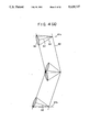
- FIG. 2 is a perspective view of a liquid crystal illustrative of the state of orientation of a chiral smectic liquid crystal having a spiral structure;
- FIG. 3 is a perspective view of a liquid crystal illustrative of the state of orientation of a chiral smectic liquid crystal having a non-spiral structure
- FIG. 4(A) is a sectional view of a chiral smectic liquid crystal oriented in accordance with the present invention
- FIG. 4(B) is a chart showing C director in a uniform orientation state of the chiral smectic liquid crystal shown in FIG. 4;
- FIG. 4(C) is a chart showing C director in a spray orientation state of the chiral smectic liquid crystal shown in FIG. 4;
- FIG. 5(A) is a plan view indicative of the tilt angle ⁇ in a uniform orientation state
- FIG. 5(B) is a plan view indicative of the tilt angle ⁇ in a spray orientation state
- FIGS. 6A-6C are schematic sectional views respectively showing the charge distribution, direction of spontaneous polarization Ps and the direction of reverse electric field Vrev in a ferroelectric liquid crystal;
- FIG. 7 is a plan view showing the change in the tilt angle ⁇ caused by application of an electric field
- FIG. 8 illustrates the optical response characteristic of a conventional liquid crystal display device
- FIG. 9 illustrates the optical response characteristic of a liquid crystal device of the present invention
- FIG. 10 is a waveform chart illustrative of the waveform of the driving voltage used in this embodiment of the present invention.
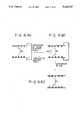
- FIG. 11 is an illustration of an embodiment of the electric system of a display apparatus incorporating a liquid crystal device of the present invention.
- FIG. 12(A) illustrates signals derived from a data modulator of the electric system during the display apparatus is driven
- FIG. 12(B) is a schematic illustration of the data modulator of FIG. 12(A).
- the liquid crystal cell in accordance with the present invention has glass plate substrates 11a and 11b covered by transparent electrodes 12a and 12b made of In 2 O 3 or ITO (Indium Tin Oxide).
- Insulating films 13a and 13b of SiO 2 , TiO 2 or Ta 2 O 5 having a thickness of 200 ⁇ to 1000 ⁇ are laminated on the transparent electrodes 12a and 12b, respectively, and orientation films 14a and 14b of 50 ⁇ to 1000 ⁇ thickness of polyimide represented by the aforementioned general formula, are laminated to the insulating films 13a and 13b, respectively.
- the orientation control films 14a and 14b have been subjected to a rubbing treatment conducted in the same parallel direction, e.g., in the direction of arrows A in FIG. 1.
- a ferroelectric smectic liquid crystal 15 is placed between the substrates 11a and 11b.
- the distance between the substrates 11a and 11b is selected to be sufficiently small so as to suppress formation of spiral structure of the ferroelectric smectic liquid crystal 15, e.g., from 0.1 ⁇ m to 3 ⁇ m.
- the liquid crystal 15 is thus held in a bistable orientation state.
- the above-mentioned small distance is conventionally preserved by bead spacers 16 such as silica or alumina beads disposed between the substrates 11a and 11b.
- the present inventors have confirmed generally that an orientation method using a specific rubbed polyimide orientation film can provide an orientation state which generates a large optical contrast between bright and dark states.
- the inventors determined that a large optical contrast is obtained between selected and non-selected pixels of the multiplexing driving method disclosed in U.S. Pat. No. 4,655,561, while eliminating any delay of optical response to, thereby obviating generation of afterimage.
- the polyimide film used in the present invention can be obtained by preparing a polyamide acid through a condensation reaction between a carboxylic acid anhydride and diamine, and heating the polyamide acid so as to close the cycle.
- Fluorine-containing diamines such as:
- the polyimide film used in the present invention may be formed by using two or more of the aforementioned carboxylic acid anhydrides and/or two or more of the aforementioned diamines.
- copolymeric condensates formed by combining a carboxylic acid selected, for example, from the following group E or a diamine selected, for example, from the following group F with the aforesaid carboxylic acid anhydride and diamine.
- thiophene-2 3, 4, 5-tetracarboxylic acid anhydride; 2, 2-bis(3, 4-biscarboxyphenyl)propane anhydride; 3, 4-dicarboxyphenylsulphone anhydride; perylene-3, 4, 9, 10-tetracarboxylic acid anhydride; bis(3, 4-dicarboxyphenyl)ether anhydride; and 3, 3', 4, 4'-benzophenone tetracarboxylic acid anhydride
- the polyimide used in the invention is characterized by containing fluorine, it is therefore preferred that the polyimide is formed using at least one of fluorine-containing carboxylic acid anhydride and fluorine-containing diamine. It is also essential that the polyimide used in the present invention has an alicyclic organic residue or an aliphatic organic residue.
- R 9 is a alicycle and R 10 is an aromatic group, at least one of R 9 and R 10 containing fluorine and n is 0 or 1.
- R 11 and R 12 are aliphatic groups, at least one of R 11 and R 12 containing fluorine and n is 0 or 1.
- R 13 is an aliphatic group
- R 14 is an alicycle, at least one of R 13 and R 14 containing fluorine and n is 0 or 1.
- R 15 is an alicycle
- R 16 is an aliphatic group, at least one of R 13 and R 14 containing fluorine and n is 0 or 1.
- the diamine used in the preparation of the polyamide acid in the present invention is used in an amount of 0.1 to 10 weight parts, preferably 1 weight part for 1 weight part of tetracarboxylic acid anhydride.
- the polyimide used in the present invention can have a mean molecular weight of 10,000 to 100,000, preferably 30,000 to 70,000, more preferably 50,000.
- the polyimide film is formed on each substrate of the liquid crystal device using a coating solution prepared by dissolving polyamide acid as a precursor of polyimide in a solvent such as dimethylformamide, dimethylacetoamide, dimethylsulfoxide or N-methylpyrrolidone.
- concentration of the polyamide acid in the solution is preferably from 0.01 to 40 wt%. .
- THe polyimide films can be formed by applying a solution of the polyimide on the substrate by a spinner coating method, spray coating method, roll applicator method or the like and heating substrate bearing the solution at a temperature of 100° to 350° C., preferably 200° to 300° C., so as to dehydrate the solution and close the cycles thereby forming the polyimide film.
- the polyimide film is then rubbed with a cloth or the like.
- the polyimide film used in the present invention has a thickness of 30 ⁇ to 1 ⁇ .
- the insulating films 13a and 13b shown in FIG. 1 may be omitted, wherein the polyimide films are preferably 200 ⁇ to 2000 ⁇ . However, when the polyimide films are formed on such insulating films 13a and 13b, the thickness of the polyimide film may preferably be from 30 ⁇ to 200 ⁇ .
- the liquid crystal used in the present invention is one that changes its state to chiral smectic phase sequentially via isotropic, cholesteric and smectic A phases in accordance with decreasing temperature. More preferably, the liquid crystal used in the invention has a pitch of at least 0.8 ⁇ m in its cholesteric phase as measured at the central temperature of the cholesteric phase temperature range. More specifically, the following liquid crystals are suitably used in the present invention.
- LC-1 (LC-1), (80B) and (80SI*) are optically active ester type ferroelectric liquid crystals. Suffixes show weight percents.
- FIG. 2 is a schematic illustration of a liquid crystal cell illustrative of the operation of a ferroelectric liquid crystal wherein 21a and 21b denote substrates coated with transparent thin film electrodes. Between the transparent electrodes is charged a liquid crystal of an SmC* (chiral smectic C) phase or SmH* (chiral smectic H) phase oriented such that the liquid crystal molecule layers 22 extend perpendicularly to the glass surfaces. Thick lines 23 represent the liquid crystal molecules and 24 denotes a bipolar moment (P ⁇ ) 24 acting in the direction perpendicular to the molecule.
- SmC* chiral smectic C
- SmH* chiral smectic H
- the liquid crystal molecule 23 has an elongated form and has a refractive anisotropy, i.e., different refractive index values in the directions of the longer and shorter axes thereof. Therefore, it is possible to obtain a liquid crystal optical modulating element which varies its optical characteristic according to the polarity of the applied voltage by placing, for example, cross-nicol polarizers on the upper and lower sides of the cell.
- the surface stable type ferroelectric liquid crystal cell which is oriented in bistable state and which is used in the liquid crystal device of the present invention can have a very small thickness of, for example, 0.1 ⁇ m to 3 ⁇ m.
- the spiral structure of the liquid crystal molecules is loosened so that a non-spiral structure is obtained even in the absence of the electric field, as shown in FIG. 3.
- the bipolar moment P or P' is directed either upward as denoted by 34a or downward as denoted by 34b.
- an electric field Ea or Eb (Ea and Eb being of opposite polarities) exceeding a predetermined threshold level is applied to the cell by the voltage applying means 31a and 31b shown in FIG. 3
- the bipolar moment is directed upward (as denoted by 34a) or downward (as denoted by 34b), whereby the liquid crystal molecules are oriented either to a first stable state 33a or the second stable state 33b.
- This ferroelectric liquid crystal cell offers two major advantages including a very high response speed as well as the bistable nature of the liquid crystal orientation, discussed below.
- the liquid crystal molecules when the electric field Ea is applied, the liquid crystal molecules are oriented to the first stable state 33a which state is stably maintained even after the application of the electric field Ea is terminated.
- the electric field Eb of the reverse polarity when the electric field Eb of the reverse polarity is applied, the liquid crystal molecules are oriented to the second stable state 33b, which state is maintained stably even after termination of the electric field Eb.
- each stable orientation state is generally maintained even when a voltage of a reverse polarity is applied, provided that the level of such voltage is below the predetermined threshold level.
- FIG. 4A is a schematic sectional view illustrating the state of orientation of liquid crystal molecules generated in the orientation direction in accordance with the present invention
- FIG. 4B is a chart showing the directions of C-directors.
- numerals 61a and 61b respectively denote upper and lower substrates and 60 designates a molecule layer composed of liquid crystal molecules 62. It is seen that the liquid crystal molecules 62 are arranged such that their positions vary along the circular bottom 64 of cone 63.
- U 1 represents a C-director 81 in one of two stable orientation states
- U 2 represents a C-director 81' in the other stable orientation state.
- the C-directors 81 and 81' are the projection of the molecule longer axis on an imaginary plane which is perpendicular to the line normal to the molecule layer 60 shown in FIG. 4A.
- FIG. 4C is a C-director chart showing the state of orientation of a rubbing-treated polyimide.
- the tilt angle ⁇ is small because the molecule axes are generally twisted between the upper and lower substrates 61a and 61b.
- FIG. 5A is a plan view illustrative of the tilt angle ⁇ when the C-director 81 is in the state shown in FIG.4B hereinafter referred to as the "uniform orientation state”
- FIG. 5B is a plan view illustrative of the tilt angle ⁇ when the C-director 81 is in the state shown in FIG.4C hereinafter referred to as the "spray orientation state”.
- numeral 50 designates the axis of rubbing treatment conducted on a specific polyimide film which meets the condition specified by the invention.
- Numerals 51a and 51b respectively denote the mean molecular axes in the orientation states U 1 and U 2 .
- Numerals 52a and 52b respectively denote the mean molecular axes in the orientation states S 1 and S 2 which switch interchangeably upon the application of threshold-exceeding voltages having opposite polarities, as do the mean molecular axes 51a and 51b.
- FIGS. 6A, 6B and 6C schematically show the distribution of charges in the liquid crystal cell, the direction of spontaneous polarization Ps and the direction of the reverse electric field. More specifically, FIG. 6A shows the state of distribution of (+) and (-) charges in the memory state before the application of a pulse electric field. In this state, the spontaneous polarization is directed from (+) charges towards (-) charges. In FIG. 6B, the direction of spontaneous polarization Ps is directed in the direction reverse to that in FIG. 6A since the liquid crystal molecules have been inverted from one stable orientation state to the other stable orientation state. Therefore, in the state shown in FIG. 6B, the (+) and (-) charges are distributed in the same manner as that shown in FIG. 6A, so that a reverse electric field Vrev is formed as indicated. After a while, this revere electric field Vrev is extinguished and the state of distribution of (+) and(-) charges becomes as shown in FIG. 6C.
- FIG. 7 shows a change in the optical response of the liquid crystal in spray orientation state generated by a conventional polyimide orientation film, in terms of a change in the tilt angle ⁇ .
- the liquid crystal material orientation respond as indicated by an arrow X 1 from the angle of the mean molecule axis S(A) in the spray orientation state "over-shooting" to the angle of the mean molecule axis U 2 of uniform orientation state near the maximum tilt angle ⁇ .
- the tilt angle ⁇ is reduced to the angle of the mean molecule axis S(B) of spray orientation state as indicated by an arrow X 2 by the action of the reverse electric field Vrev.
- the orientation provided by the effect of the aforementioned fluorine-containing polyimide film precludes the generation of the mean molecule axes S(A), S(B) and S(C) of in FIG. 7, so that the molecules can be oriented to have such a mean molecule axis that produces a tilt angle ⁇ approximating the maximum tilt angle ⁇ .
- the optical response characteristic of the liquid crystal device of the present invention having the above-mentioned feature is shown in FIG. 9. From FIG. 9, it will be understood that the liquid crystal device does not suffer from any delay in the optical response from which an afterimage is generated, and that the liquid crystal device of the present invention provides a display with a high contrast.
- alumina beads of a mean particle size of 1.5 ⁇ m were sprayed on one of the glass sheets and the pair of substrates were superposed such that the directions of the axes of rubbing treatments on both substrates are parallel to and in the same direction as each other, thus forming a cell structure.
- the cell was then charged with the ferroelectric smectic liquid crystal "CS-1014" (discussed previously) in an isotropic phase by vacuum injection.
- the liquid crystal was cooled slowly from the isotropic phase temperature at a rate of 0.5° C./h down to 30° C. whereby the liquid crystal was oriented.
- the liquid crystal "CS-1014" used in the liquid crystal cell of this example showed the following phase change. ##STR14## wherein Iso represents isotropic phase, Ch represents cholesteric phase, SmA represents smectic A phase and SmC* represents chiral smectic C phase.
- the thus formed liquid crystal cell was sandwiched between a pair of cross-nicol polarizing elements and a 50 ⁇ sec pulse of 30 V was applied to the liquid crystal cell while the 90° cross-nicol was set to darkest (light extinction) state.
- the light transmittance of the liquid crystal cell in this state was measured with a photomultiplator and a 50 ⁇ sec pulse of -30V was then applied to realize a bright state and the transmittance in this state was again measured by the same method. It was confirmed that the tilt angle was 15° and the values of transmittance in the darkest and the bright states were respectively 0.9% and 45%, thus providing a contrast ratio of 50:1.
- the delay of optical response which results in the generation of an afterimage was as short as 0.2 seconds.
- FIG. 10 A multiplexing driving of this liquid crystal cell was conducted using the driving waveforms as shown in FIG. 10 which results in a display with a high quality of image and a high contrast.
- certain characters were input and displayed, after which the entire display area was erased to white state. No visible after image was observed after the extinction of the characters.
- S N , S N+1 and S N+2 represent waveforms of voltages applied to the scanning lines, and I shows the waveform of a voltage applied to a representative data line.
- (I -S n ) represents the composite waveform obtained at the point of intersection of the data line I and the scanning line S N .
- the voltage V 0 was set to range between 5V and 8V, while the duration ⁇ T was set to be from 20 ⁇ sec to 70 ⁇ sec.
- Liquid crystal cells were produced by the same process as Example 1, except for using orientation control films (polyimide molecules having mean molecular weight of 50,000) and the liquid crystal materials shown in Table 1 below.
- orientation control films polyimide molecules having mean molecular weight of 50,000
- Example 1 These liquid crystal cells were subjected to a same multiplexing driving display test conducted under the same conditions as Example 1. All these Examples showed superior display performance similar to that of Example 1.
- Liquid crystal cells were produced in the same manner as Example 1 except that the orientation control films and liquid crystal materials shown in Table 3 below were used. The contrast ratio and the delay of optical response were measured on these liquid crystal cells to obtain the results shown in Table 4 below.
- liquid crystal cells were subjected to a multiplexing driving display test conducted under the same conditions as Example 1. These liquid crystal cells showed significantly smaller contrast ratio values than in those of Examples 1 to 6 produced in accordance with the invention. In addition, the significantly slower optical response characteristic provided that afterimage was observed in the Comparative Examples.
- FIG. 11 shows, in simplified form, one embodiment of electric system for driving a liquid crystal device of the invention mounted in a display apparatus wherein signals for the scanning electrodes are formed by sending clock signals CS (generated by a clock generator) to a scanning electrode selector (for selecting scanning electrodes) and then delivering the output from the scanning electrode selector to a scanning electrode driver.
- Signals DM for the signal electrodes are formed by delivering output signal DS (from a data generator) and clock signals CS to a data modulator.
- the data modulator can produce both data and auxiliary signals, which are then supplied to a signal electrode driver.
- FIG. 12A shows Examples of signals output from the above-mentioned data modulator
- FIG. 12B schematically shows the data modulator for generating the signals shown in FIG. 12A.
- the data modulator has a pair of inverters 121 and 122, a pair of AND circuits 123 and 124 and an OR circuit 125.
- a uniform orientation of the ferroelectric liquid crystal can be attained without requiring any treatment prior to application of A.C. driving power, by virtue of the use of the orientation film made from fluorine-containing alicyclic or aliphatic polyimide which is a critical feature of the present invention.
- liquid crystal device which exhibits a high contrast between bright and dark states particularly in multiplexing driving mode and which can eliminate generation of after image.
Landscapes
- Chemical & Material Sciences (AREA)
- Physics & Mathematics (AREA)
- Organic Chemistry (AREA)
- Nonlinear Science (AREA)
- Crystallography & Structural Chemistry (AREA)
- Mathematical Physics (AREA)
- Polymers & Plastics (AREA)
- Spectroscopy & Molecular Physics (AREA)
- Health & Medical Sciences (AREA)
- Medicinal Chemistry (AREA)
- Chemical Kinetics & Catalysis (AREA)
- General Physics & Mathematics (AREA)
- Optics & Photonics (AREA)
- Engineering & Computer Science (AREA)
- Materials Engineering (AREA)
- Liquid Crystal (AREA)
- Macromolecular Compounds Obtained By Forming Nitrogen-Containing Linkages In General (AREA)
Applications Claiming Priority (4)
| Application Number | Priority Date | Filing Date | Title |
|---|---|---|---|
| JP2-089402 | 1990-04-03 | ||
| JP8940290 | 1990-04-03 | ||
| JP2-041800 | 1991-03-07 | ||
| JP3041800A JPH04212127A (ja) | 1990-04-03 | 1991-03-07 | 液晶素子および表示装置 |
Publications (1)
| Publication Number | Publication Date |
|---|---|
| US5129727A true US5129727A (en) | 1992-07-14 |
Family
ID=26381469
Family Applications (1)
| Application Number | Title | Priority Date | Filing Date |
|---|---|---|---|
| US07/676,519 Expired - Fee Related US5129727A (en) | 1990-04-03 | 1991-03-28 | Liquid crystal device having the orientation control films which comprise a fluorine-containing aliphatic or alicyclic polyimide and display apparatus |
Country Status (5)
| Country | Link |
|---|---|
| US (1) | US5129727A (de) |
| EP (1) | EP0450549B1 (de) |
| JP (1) | JPH04212127A (de) |
| AT (1) | ATE158091T1 (de) |
| DE (1) | DE69127569T2 (de) |
Cited By (31)
| Publication number | Priority date | Publication date | Assignee | Title |
|---|---|---|---|---|
| US5268780A (en) * | 1989-05-11 | 1993-12-07 | Canon Kabushiki Kaisha | Liquid crystal device having a polyimide alignment film substituted with fluorine or a fluorine-containing group |
| US5320883A (en) * | 1991-10-22 | 1994-06-14 | Canon Kabushiki Kaisha | Liquid crystal device |
| US5325219A (en) * | 1991-10-30 | 1994-06-28 | Canon Kabushiki Kaisha | Chiral smectic liquid crystal device having polyimide alignment layer with fluoroalkyl side chain |
| US5326600A (en) * | 1991-11-08 | 1994-07-05 | Canon Kabushiki Kaisha | Liquid crystal device |
| US5330803A (en) * | 1991-08-06 | 1994-07-19 | Canon Kabushiki Kaisha | Liquid crystal device |
| US5381256A (en) * | 1991-12-10 | 1995-01-10 | Canon Kabushiki Kaisha | Ferroelectric liquid crystal device with fine particles on insulator, having diameter less than substrate gap |
| US5400159A (en) * | 1991-08-06 | 1995-03-21 | Canon Kabushiki Kaisha | Liquid crystal device having alignment film with particular surface energy difference before and after rubbing |
| US5419931A (en) * | 1992-09-18 | 1995-05-30 | Canon Kabushiki Kaisha | Liquid crystal device |
| US5422749A (en) * | 1987-09-17 | 1995-06-06 | Canon Kabushiki Kaisha | Ferroelectric smetic liquid crystal device |
| US5426525A (en) * | 1987-09-17 | 1995-06-20 | Canon Kabushiki Kaisha | Ferroelectric smectic liquid crystal device |
| US5464668A (en) * | 1992-02-05 | 1995-11-07 | Canon Kabushiki Kaisha | Liquid crystal device |
| US5518782A (en) * | 1992-12-14 | 1996-05-21 | Canon Kabushiki Kaisha | Liquid crystal device |
| US5520845A (en) * | 1993-12-02 | 1996-05-28 | E. I. Du Pont De Nemours And Company | Poly(2,6-piperazinedione) alignment layer for liquid crystal displays |
| US5543943A (en) * | 1992-01-24 | 1996-08-06 | Canon Kabushiki Kaisha | Chiral smectic device subjected to a simultaneous thermal and AC field treatment |
| US5576864A (en) * | 1984-07-11 | 1996-11-19 | Canon Kabushiki Kaisha | Chiral smectic liquid crystal device having fluorine-containing polymeric alignment film with predetermined refractive index anisotropy after rubbing |
| US5587211A (en) * | 1994-04-18 | 1996-12-24 | Canon Kabushiki Kaisha | Liquid crystal device and liquid crystal apparatus including same |
| US5594571A (en) * | 1991-12-10 | 1997-01-14 | Canon Kabushiki Kaisha | Ferroelectric liquid crystal device and process for production thereof |
| US5611941A (en) * | 1995-07-17 | 1997-03-18 | Rainbow Display Serivices | Method for forming a ferroelectric liquid crystal spatial light modulator utilizing a planarization process |
| US5626925A (en) * | 1992-02-05 | 1997-05-06 | Canon Kabushiki Kaisha | Liquid crystal device |
| US5690858A (en) * | 1992-11-25 | 1997-11-25 | Canon Kabushiki Kaisha | Mesomorphic compound, liquid crystal composition and liquid crystal device |
| US5698135A (en) * | 1994-12-16 | 1997-12-16 | Japan Synthetic Rubber Co., Ltd., A Japanese Corporation | Liquid crystal-aligning agent |
| US5714209A (en) * | 1992-02-05 | 1998-02-03 | Canon Kabushiki Kaisha | Liquid crystal device |
| US5841497A (en) * | 1995-07-28 | 1998-11-24 | Canon Kabushiki Kaisha | Liquid crystal device and liquid crystal apparatus |
| US5858273A (en) * | 1995-07-27 | 1999-01-12 | Canon Kabushiki Kaisha | Liquid crystal device |
| US5885482A (en) * | 1995-12-28 | 1999-03-23 | Canon Kabushiki Kaisha | Liquid crystal device, production process thereof and liquid crystal apparatus |
| US6001276A (en) * | 1996-07-22 | 1999-12-14 | Canon Kabishiki Kaisha | Liquid crystal device |
| US6067139A (en) * | 1997-06-26 | 2000-05-23 | E. I. Du Pont De Nemours And Company | Multi-domain STN LCD comprising fluorinated polyimide alignment layers |
| US6194039B1 (en) * | 1999-10-22 | 2001-02-27 | Elsicon, Inc. | Materials for inducing alignment in liquid crystals and liquid crystal displays |
| US6340506B1 (en) | 1997-09-25 | 2002-01-22 | Rolic Ag | Photocrosslinkable polyimides |
| US6348245B1 (en) * | 1998-05-21 | 2002-02-19 | E. I. Du Pont De Nemours And Company | Polymide photo alignment film from 3,3′,4,4′-benzophenone tetracarboxylic dianhydride and ortho-substituted aromatic diamines for liquid crystal displays |
| US6747715B2 (en) * | 2000-12-04 | 2004-06-08 | Kabushiki Kaisha Toshiba | Polarized light reflecting element, liquid crystal display element using the same, and method of manufacturing polarized light reflecting element |
Families Citing this family (11)
| Publication number | Priority date | Publication date | Assignee | Title |
|---|---|---|---|---|
| CA2099437A1 (en) * | 1992-07-17 | 1994-01-18 | Marc D. Radcliffe | Liquid crystal display device |
| US7972725B2 (en) * | 2004-11-08 | 2011-07-05 | 3M Innovative Properties Company | Polyimide electrode binders |
| US9627722B1 (en) | 2013-09-16 | 2017-04-18 | American Lithium Energy Corporation | Positive temperature coefficient film, positive temperature coefficient electrode, positive temperature coefficient separator, and battery comprising the same |
| CN115603009A (zh) | 2014-11-25 | 2023-01-13 | 美国锂能源公司(Us) | 配置在可充电电池中的保护层、可充电电池及方法 |
| US10020545B2 (en) | 2014-11-25 | 2018-07-10 | American Lithium Energy Corporation | Rechargeable battery with resistive layer for enhanced safety |
| US10020487B2 (en) | 2014-11-25 | 2018-07-10 | American Lithium Energy Corporation | Rechargeable battery with voltage activated current interrupter |
| US10396341B2 (en) | 2014-11-25 | 2019-08-27 | American Lithium Energy Corporation | Rechargeable battery with internal current limiter and interrupter |
| US10483523B2 (en) | 2016-02-19 | 2019-11-19 | American Lithium Energy Corporation | Dual function current collector |
| EP3869600B1 (de) | 2017-05-01 | 2022-10-19 | American Lithium Energy Corporation | Stromversorgungssystem und sicherung aufweisend eine platte mit negativer wärmeausdehnung |
| US10923727B2 (en) | 2017-07-28 | 2021-02-16 | American Lithium Energy Corporation | Anti-corrosion for battery current collector |
| US12230844B2 (en) | 2018-06-25 | 2025-02-18 | American Lithium Energy Corporation | Safety layer for battery cells |
Citations (5)
| Publication number | Priority date | Publication date | Assignee | Title |
|---|---|---|---|---|
| US4367924A (en) * | 1980-01-08 | 1983-01-11 | Clark Noel A | Chiral smectic C or H liquid crystal electro-optical device |
| GB2174399A (en) * | 1985-03-10 | 1986-11-05 | Nitto Electric Ind Co | Colorless transparent polyimide shaped articles and their production |
| EP0231781A1 (de) * | 1986-01-22 | 1987-08-12 | Hitachi, Ltd. | Flüssigkristallanzeigeelement |
| US4828754A (en) * | 1985-01-09 | 1989-05-09 | Dainippon Ink & Chemicals, Inc. | Novel liquid crystalline compounds having substituents |
| US4879059A (en) * | 1986-09-02 | 1989-11-07 | Canon Kabushiki Kaisha | Liquid crystal device |
-
1991
- 1991-03-07 JP JP3041800A patent/JPH04212127A/ja active Pending
- 1991-03-28 US US07/676,519 patent/US5129727A/en not_active Expired - Fee Related
- 1991-04-02 DE DE69127569T patent/DE69127569T2/de not_active Expired - Fee Related
- 1991-04-02 AT AT91105152T patent/ATE158091T1/de not_active IP Right Cessation
- 1991-04-02 EP EP91105152A patent/EP0450549B1/de not_active Expired - Lifetime
Patent Citations (5)
| Publication number | Priority date | Publication date | Assignee | Title |
|---|---|---|---|---|
| US4367924A (en) * | 1980-01-08 | 1983-01-11 | Clark Noel A | Chiral smectic C or H liquid crystal electro-optical device |
| US4828754A (en) * | 1985-01-09 | 1989-05-09 | Dainippon Ink & Chemicals, Inc. | Novel liquid crystalline compounds having substituents |
| GB2174399A (en) * | 1985-03-10 | 1986-11-05 | Nitto Electric Ind Co | Colorless transparent polyimide shaped articles and their production |
| EP0231781A1 (de) * | 1986-01-22 | 1987-08-12 | Hitachi, Ltd. | Flüssigkristallanzeigeelement |
| US4879059A (en) * | 1986-09-02 | 1989-11-07 | Canon Kabushiki Kaisha | Liquid crystal device |
Cited By (39)
| Publication number | Priority date | Publication date | Assignee | Title |
|---|---|---|---|---|
| US5576864A (en) * | 1984-07-11 | 1996-11-19 | Canon Kabushiki Kaisha | Chiral smectic liquid crystal device having fluorine-containing polymeric alignment film with predetermined refractive index anisotropy after rubbing |
| US5422749A (en) * | 1987-09-17 | 1995-06-06 | Canon Kabushiki Kaisha | Ferroelectric smetic liquid crystal device |
| US5426525A (en) * | 1987-09-17 | 1995-06-20 | Canon Kabushiki Kaisha | Ferroelectric smectic liquid crystal device |
| US5268780A (en) * | 1989-05-11 | 1993-12-07 | Canon Kabushiki Kaisha | Liquid crystal device having a polyimide alignment film substituted with fluorine or a fluorine-containing group |
| US5510159A (en) * | 1991-01-22 | 1996-04-23 | Canon Kabushiki Kaisha | Liquid crystal device |
| US5330803A (en) * | 1991-08-06 | 1994-07-19 | Canon Kabushiki Kaisha | Liquid crystal device |
| US5400159A (en) * | 1991-08-06 | 1995-03-21 | Canon Kabushiki Kaisha | Liquid crystal device having alignment film with particular surface energy difference before and after rubbing |
| US5320883A (en) * | 1991-10-22 | 1994-06-14 | Canon Kabushiki Kaisha | Liquid crystal device |
| US5325219A (en) * | 1991-10-30 | 1994-06-28 | Canon Kabushiki Kaisha | Chiral smectic liquid crystal device having polyimide alignment layer with fluoroalkyl side chain |
| US5326600A (en) * | 1991-11-08 | 1994-07-05 | Canon Kabushiki Kaisha | Liquid crystal device |
| US5835248A (en) * | 1991-12-10 | 1998-11-10 | Canon Kabushiki Kaisha | Method of making ferroelectric liquid crystal device using particles to create an unevenness on alignment layer or underlying insulating layer |
| US5764327A (en) * | 1991-12-10 | 1998-06-09 | Canon Kabushiki Kaisha | Ferroelectric liquid crystal device with uneven surface under alignment film and process for production |
| US5381256A (en) * | 1991-12-10 | 1995-01-10 | Canon Kabushiki Kaisha | Ferroelectric liquid crystal device with fine particles on insulator, having diameter less than substrate gap |
| US5594571A (en) * | 1991-12-10 | 1997-01-14 | Canon Kabushiki Kaisha | Ferroelectric liquid crystal device and process for production thereof |
| US5543943A (en) * | 1992-01-24 | 1996-08-06 | Canon Kabushiki Kaisha | Chiral smectic device subjected to a simultaneous thermal and AC field treatment |
| US5790223A (en) * | 1992-01-24 | 1998-08-04 | Canon Kabushiki Kaisha | Ferroelectric liquid crystal device and treatment method therefor |
| US5464668A (en) * | 1992-02-05 | 1995-11-07 | Canon Kabushiki Kaisha | Liquid crystal device |
| US5626925A (en) * | 1992-02-05 | 1997-05-06 | Canon Kabushiki Kaisha | Liquid crystal device |
| US5714209A (en) * | 1992-02-05 | 1998-02-03 | Canon Kabushiki Kaisha | Liquid crystal device |
| US5552193A (en) * | 1992-09-18 | 1996-09-03 | Canon Kabushiki Kaisha | Liquid crystal device |
| US5571580A (en) * | 1992-09-18 | 1996-11-05 | Canon Kabushiki Kaisha | Liquid crystal device |
| US5419931A (en) * | 1992-09-18 | 1995-05-30 | Canon Kabushiki Kaisha | Liquid crystal device |
| US5690858A (en) * | 1992-11-25 | 1997-11-25 | Canon Kabushiki Kaisha | Mesomorphic compound, liquid crystal composition and liquid crystal device |
| US5518782A (en) * | 1992-12-14 | 1996-05-21 | Canon Kabushiki Kaisha | Liquid crystal device |
| US5520845A (en) * | 1993-12-02 | 1996-05-28 | E. I. Du Pont De Nemours And Company | Poly(2,6-piperazinedione) alignment layer for liquid crystal displays |
| US5587211A (en) * | 1994-04-18 | 1996-12-24 | Canon Kabushiki Kaisha | Liquid crystal device and liquid crystal apparatus including same |
| US5698135A (en) * | 1994-12-16 | 1997-12-16 | Japan Synthetic Rubber Co., Ltd., A Japanese Corporation | Liquid crystal-aligning agent |
| US5611941A (en) * | 1995-07-17 | 1997-03-18 | Rainbow Display Serivices | Method for forming a ferroelectric liquid crystal spatial light modulator utilizing a planarization process |
| US5858273A (en) * | 1995-07-27 | 1999-01-12 | Canon Kabushiki Kaisha | Liquid crystal device |
| US5841497A (en) * | 1995-07-28 | 1998-11-24 | Canon Kabushiki Kaisha | Liquid crystal device and liquid crystal apparatus |
| US5885482A (en) * | 1995-12-28 | 1999-03-23 | Canon Kabushiki Kaisha | Liquid crystal device, production process thereof and liquid crystal apparatus |
| US6001276A (en) * | 1996-07-22 | 1999-12-14 | Canon Kabishiki Kaisha | Liquid crystal device |
| US6067139A (en) * | 1997-06-26 | 2000-05-23 | E. I. Du Pont De Nemours And Company | Multi-domain STN LCD comprising fluorinated polyimide alignment layers |
| US6340506B1 (en) | 1997-09-25 | 2002-01-22 | Rolic Ag | Photocrosslinkable polyimides |
| US6348245B1 (en) * | 1998-05-21 | 2002-02-19 | E. I. Du Pont De Nemours And Company | Polymide photo alignment film from 3,3′,4,4′-benzophenone tetracarboxylic dianhydride and ortho-substituted aromatic diamines for liquid crystal displays |
| US6194039B1 (en) * | 1999-10-22 | 2001-02-27 | Elsicon, Inc. | Materials for inducing alignment in liquid crystals and liquid crystal displays |
| WO2001030938A1 (en) * | 1999-10-22 | 2001-05-03 | Elsicon, Inc. | Materials for inducing alignment in liquid crystals and liquid crystal displays |
| US6713135B2 (en) * | 1999-10-22 | 2004-03-30 | Elsicon, Inc. | Materials for inducing alignment in liquid crystals and liquid crystal displays |
| US6747715B2 (en) * | 2000-12-04 | 2004-06-08 | Kabushiki Kaisha Toshiba | Polarized light reflecting element, liquid crystal display element using the same, and method of manufacturing polarized light reflecting element |
Also Published As
| Publication number | Publication date |
|---|---|
| EP0450549A1 (de) | 1991-10-09 |
| EP0450549B1 (de) | 1997-09-10 |
| JPH04212127A (ja) | 1992-08-03 |
| DE69127569T2 (de) | 1998-02-26 |
| DE69127569D1 (de) | 1997-10-16 |
| ATE158091T1 (de) | 1997-09-15 |
Similar Documents
| Publication | Publication Date | Title |
|---|---|---|
| US5129727A (en) | Liquid crystal device having the orientation control films which comprise a fluorine-containing aliphatic or alicyclic polyimide and display apparatus | |
| US5046822A (en) | Liquid crystal device | |
| EP0400635B1 (de) | Flüssigkristall-Vorrichtung | |
| US5268780A (en) | Liquid crystal device having a polyimide alignment film substituted with fluorine or a fluorine-containing group | |
| US5326600A (en) | Liquid crystal device | |
| US5510159A (en) | Liquid crystal device | |
| US5330803A (en) | Liquid crystal device | |
| US5400159A (en) | Liquid crystal device having alignment film with particular surface energy difference before and after rubbing | |
| US5576864A (en) | Chiral smectic liquid crystal device having fluorine-containing polymeric alignment film with predetermined refractive index anisotropy after rubbing | |
| US5419931A (en) | Liquid crystal device | |
| US5464668A (en) | Liquid crystal device | |
| US5250330A (en) | Liquid crystal device | |
| JP2556590B2 (ja) | 液晶素子 | |
| EP0397153A2 (de) | Chiralsmektische Flüssigkristallvorrichtung | |
| US5518782A (en) | Liquid crystal device | |
| JP2556604B2 (ja) | 液晶素子 | |
| US5626925A (en) | Liquid crystal device | |
| US5714209A (en) | Liquid crystal device | |
| JP2567128B2 (ja) | 液晶素子 | |
| JP2675893B2 (ja) | 液晶素子 | |
| JP2556586B2 (ja) | 液晶素子 | |
| JP2556581B2 (ja) | 液晶素子 | |
| JP2556584B2 (ja) | 液晶素子 | |
| JP2556587B2 (ja) | 液晶素子 | |
| JP2556582B2 (ja) | 液晶素子 |
Legal Events
| Date | Code | Title | Description |
|---|---|---|---|
| AS | Assignment |
Owner name: CANON KABUSHIKI KAISHA A CORPORATION OF JAPAN, JA Free format text: ASSIGNMENT OF ASSIGNORS INTEREST.;ASSIGNORS:HANYU, YUKIO;ASAOKA, MASANOBU;REEL/FRAME:005729/0043 Effective date: 19910513 |
|
| CC | Certificate of correction | ||
| FPAY | Fee payment |
Year of fee payment: 4 |
|
| FEPP | Fee payment procedure |
Free format text: PAYER NUMBER DE-ASSIGNED (ORIGINAL EVENT CODE: RMPN); ENTITY STATUS OF PATENT OWNER: LARGE ENTITY |
|
| FEPP | Fee payment procedure |
Free format text: PAYOR NUMBER ASSIGNED (ORIGINAL EVENT CODE: ASPN); ENTITY STATUS OF PATENT OWNER: LARGE ENTITY |
|
| FPAY | Fee payment |
Year of fee payment: 8 |
|
| REMI | Maintenance fee reminder mailed | ||
| LAPS | Lapse for failure to pay maintenance fees | ||
| FP | Lapsed due to failure to pay maintenance fee |
Effective date: 20040714 |
|
| STCH | Information on status: patent discontinuation |
Free format text: PATENT EXPIRED DUE TO NONPAYMENT OF MAINTENANCE FEES UNDER 37 CFR 1.362 |