US5037168A - Optical waveguides - Google Patents
Optical waveguides Download PDFInfo
- Publication number
- US5037168A US5037168A US07/400,652 US40065289A US5037168A US 5037168 A US5037168 A US 5037168A US 40065289 A US40065289 A US 40065289A US 5037168 A US5037168 A US 5037168A
- Authority
- US
- United States
- Prior art keywords
- refractive index
- layer
- buffer layer
- channel
- substrate
- Prior art date
- Legal status (The legal status is an assumption and is not a legal conclusion. Google has not performed a legal analysis and makes no representation as to the accuracy of the status listed.)
- Expired - Fee Related
Links
Images
Classifications
-
- G—PHYSICS
- G02—OPTICS
- G02F—OPTICAL DEVICES OR ARRANGEMENTS FOR THE CONTROL OF LIGHT BY MODIFICATION OF THE OPTICAL PROPERTIES OF THE MEDIA OF THE ELEMENTS INVOLVED THEREIN; NON-LINEAR OPTICS; FREQUENCY-CHANGING OF LIGHT; OPTICAL LOGIC ELEMENTS; OPTICAL ANALOGUE/DIGITAL CONVERTERS
- G02F1/00—Devices or arrangements for the control of the intensity, colour, phase, polarisation or direction of light arriving from an independent light source, e.g. switching, gating or modulating; Non-linear optics
- G02F1/01—Devices or arrangements for the control of the intensity, colour, phase, polarisation or direction of light arriving from an independent light source, e.g. switching, gating or modulating; Non-linear optics for the control of the intensity, phase, polarisation or colour
- G02F1/061—Devices or arrangements for the control of the intensity, colour, phase, polarisation or direction of light arriving from an independent light source, e.g. switching, gating or modulating; Non-linear optics for the control of the intensity, phase, polarisation or colour based on electro-optical organic material
- G02F1/065—Devices or arrangements for the control of the intensity, colour, phase, polarisation or direction of light arriving from an independent light source, e.g. switching, gating or modulating; Non-linear optics for the control of the intensity, phase, polarisation or colour based on electro-optical organic material in an optical waveguide structure
-
- G—PHYSICS
- G02—OPTICS
- G02B—OPTICAL ELEMENTS, SYSTEMS OR APPARATUS
- G02B6/00—Light guides; Structural details of arrangements comprising light guides and other optical elements, e.g. couplings
- G02B6/10—Light guides; Structural details of arrangements comprising light guides and other optical elements, e.g. couplings of the optical waveguide type
- G02B6/12—Light guides; Structural details of arrangements comprising light guides and other optical elements, e.g. couplings of the optical waveguide type of the integrated circuit kind
- G02B6/122—Basic optical elements, e.g. light-guiding paths
Definitions
- This invention relates to an optical waveguide and to methods of forming optical waveguides.
- An optical waveguide is an elongate structure providing two-dimensional confinement of light in its transverse plane.
- Electro-optically active polymers show great potential for making high speed integrated optical modulators and switches.
- a high speed optical modulator for example, an electrode structure is included which normally supports a microwave mode. This mode will ideally travel collinearly with the optical signal, yielding an electro-optically induced phase advance or retardation with distance.
- one of the main loss mechanisms is side wall roughness.
- Surface roughness due to the etching techniques used to define the waveguide structure typically have RMS standard deviations of a few to a few hundred nanometers.
- the waveguide is formed by producing a channel in a substrate by processes such as reactive ion etching, with the active polymer then being provided in the channel, the etching processes leave a rough side wall finish.
- processes such as reactive ion etching
- the active polymer then being provided in the channel
- the etching processes leave a rough side wall finish.
- multi-layer polymer structures where some etchant or solvent is used to cut through one layer in the waveguide region. Such layers are typically fabricated by dip or spin coating.
- the present invention provides, in one aspect, an optical waveguide, comprising an elongate body of an active waveguiding material of first refractive index surrounded by material of lower refractive index, and a smoothing layer between at least a portion of the surface of the elongate body and the surrounding material, the smoothing layer being such as to produce an interface of substantially reduced roughness between the material of first refractive index and material having a lower refractive index.
- At least part of the elongate body of waveguiding material is located in a channel defined by material of lower refractive index.
- Another aspect of the invention provides a method of forming an optical waveguide, comprising forming a channel in a substrate, providing a smoothing layer on at least a portion of the walls of the channel, thereby substantially reducing the surface roughness of the walls, and filling the channel with a waveguiding medium having a higher refractive index than those of the smoothing layer and the substrate.
- the smoothing layer is preferably very thin, and may be provided by spin coating with a polymer solution. Ideally, the thickness of the smoothing layer is sufficient to fill the microscopic roughnesses of the side walls, while being substantially smaller than the cross-sectional dimensions of the waveguides. A substantial reduction in signal losses along the waveguide may be achieved by the use of the smoothing layer in accordance with the invention.
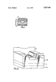
- FIG. 1 is a schematic sectional elevation of a waveguide according to one embodiment of the invention.
- FIG. 2 is a perspective view, on an enlarged scale, of a section of the waveguide shown in FIG. 1.
- FIG. 1 illustrates an inverted rib waveguide comprising a substrate 10, which may have an overlying electrode layer 11, for example of gold, and a buffer layer 12 having a refractive index n 2 .
- the buffer layer 12 is formed by growing a crystalline body of silicon oxynitride (SiON), the substrate 10, electrode layer 11 and buffer layer 12 forming a substrate member.
- a channel 13 (FIG. 2) is formed in the buffer layer 12 by reactive ion etching to a suitable dept, the dimensions of the channel being such that the waveguide formed therein gives a single mode structure. The etching leaves roughness, particularly on the walls of the channel 13, shown in exaggerated form in FIG. 2.
- a smoothing layer 14 is formed on the surface of the buffer layer 12, by spin or dip coating of a solution of a polymer having a refractive index as close as possible to the refractive index n 2 of the buffer layer.
- a solution of 5% by weight of polyvinyl benzyl chloride in toluene may be used for the dip coating.
- the layer is cured by baking at 140° C. in vacuo for 16 hours, followed by a further hour at 200° C.
- a layer 15 of active waveguiding polymeric material is then coated onto the surface of the smoothing layer.
- the material of this layer 15 has a higher refractive index n 1 than the refractive index of the buffer layer n 2 .
- a further buffer layer 16 of polymeric material is provided over the layer of the active waveguiding material 15.
- This further buffer layer has a lower refractive index n 3 which may be close to that of the first buffer layer 12.
- a second electrode layer 17 can be provided on top of the buffer layer 16.
- the first buffer layer 12 could also be formed of a polymeric material, in which case the smoothing layer may be of a material which can be coated on to the buffer layer without substantial dissolution thereof.
- the smoothing layer may comprise the same polymer as is used to form the buffer layer.
Abstract
A smoothing layer is provided between the rough etched sides of a channel in a substrate in which an optical waveguiding material is to be produced. Losses are substantially reduced thereby. For a rectangular or rib waveguide, where the sides of the rib are left rough by etching, a smoothing layer is again provided over the rib. The smoothing layer preferably has a refractive index close to or the same as the materials having surface roughness.
Description
1. Background of the Invention
This invention relates to an optical waveguide and to methods of forming optical waveguides.
An optical waveguide is an elongate structure providing two-dimensional confinement of light in its transverse plane.
2. Description of the Prior Art
Electro-optically active polymers show great potential for making high speed integrated optical modulators and switches. In a high speed optical modulator, for example, an electrode structure is included which normally supports a microwave mode. This mode will ideally travel collinearly with the optical signal, yielding an electro-optically induced phase advance or retardation with distance.
In making polymer waveguides for integrated optical modulators, for example, one of the main loss mechanisms is side wall roughness. Surface roughness due to the etching techniques used to define the waveguide structure typically have RMS standard deviations of a few to a few hundred nanometers.
For example, where the waveguide is formed by producing a channel in a substrate by processes such as reactive ion etching, with the active polymer then being provided in the channel, the etching processes leave a rough side wall finish. This is also true for multi-layer polymer structures where some etchant or solvent is used to cut through one layer in the waveguide region. Such layers are typically fabricated by dip or spin coating.
The present invention provides, in one aspect, an optical waveguide, comprising an elongate body of an active waveguiding material of first refractive index surrounded by material of lower refractive index, and a smoothing layer between at least a portion of the surface of the elongate body and the surrounding material, the smoothing layer being such as to produce an interface of substantially reduced roughness between the material of first refractive index and material having a lower refractive index.
At least part of the elongate body of waveguiding material is located in a channel defined by material of lower refractive index.
Another aspect of the invention provides a method of forming an optical waveguide, comprising forming a channel in a substrate, providing a smoothing layer on at least a portion of the walls of the channel, thereby substantially reducing the surface roughness of the walls, and filling the channel with a waveguiding medium having a higher refractive index than those of the smoothing layer and the substrate.
The smoothing layer is preferably very thin, and may be provided by spin coating with a polymer solution. Ideally, the thickness of the smoothing layer is sufficient to fill the microscopic roughnesses of the side walls, while being substantially smaller than the cross-sectional dimensions of the waveguides. A substantial reduction in signal losses along the waveguide may be achieved by the use of the smoothing layer in accordance with the invention.
FIG. 1 is a schematic sectional elevation of a waveguide according to one embodiment of the invention; and
FIG. 2 is a perspective view, on an enlarged scale, of a section of the waveguide shown in FIG. 1.
FIG. 1 illustrates an inverted rib waveguide comprising a substrate 10, which may have an overlying electrode layer 11, for example of gold, and a buffer layer 12 having a refractive index n2. The buffer layer 12 is formed by growing a crystalline body of silicon oxynitride (SiON), the substrate 10, electrode layer 11 and buffer layer 12 forming a substrate member. A channel 13 (FIG. 2) is formed in the buffer layer 12 by reactive ion etching to a suitable dept, the dimensions of the channel being such that the waveguide formed therein gives a single mode structure. The etching leaves roughness, particularly on the walls of the channel 13, shown in exaggerated form in FIG. 2. A smoothing layer 14 is formed on the surface of the buffer layer 12, by spin or dip coating of a solution of a polymer having a refractive index as close as possible to the refractive index n2 of the buffer layer. A solution of 5% by weight of polyvinyl benzyl chloride in toluene may be used for the dip coating. The layer is cured by baking at 140° C. in vacuo for 16 hours, followed by a further hour at 200° C.
A layer 15 of active waveguiding polymeric material is then coated onto the surface of the smoothing layer. The material of this layer 15 has a higher refractive index n1 than the refractive index of the buffer layer n2. Finally, as may be seen from FIG. 1, a further buffer layer 16 of polymeric material is provided over the layer of the active waveguiding material 15. This further buffer layer has a lower refractive index n3 which may be close to that of the first buffer layer 12. A second electrode layer 17 can be provided on top of the buffer layer 16. It will be appreciated that the first buffer layer 12 could also be formed of a polymeric material, in which case the smoothing layer may be of a material which can be coated on to the buffer layer without substantial dissolution thereof. Where the polymeric buffer layer can be subjected to a suitable curing process to minimise dissolution effects, the smoothing layer may comprise the same polymer as is used to form the buffer layer.
Claims (9)
1. An optical waveguide comprising
an elongate body of an active polymeric waveguiding material of first refractive index located in a channel formed in a substrate material of lower refractive index; and
a polymeric smoothing layer having a lower refractive index than said waveguiding material, said smoothing layer being located in said channel between said elongate body and said substrate material.
2. An optical waveguide according to claim 1, wherein said smoothing layer comprises a material having a refractive index substantially equal to that of said substrate material.
3. An optical waveguide comprising:
a substrate member including a first buffer layer having a channel therein defined by a wall of given roughness, said first buffer layer having a refractive index n2 ;
an elongate body composed of an active polymeric waveguiding material located in said channel, said elongate body having a refractive index n1, where n1 is greater than n2 ;
a polymeric smoothing layer located in said channel between said elongate body and said first buffer layer, said smoothing layer having a refractive index which is lower than the refractive index n1 of said first buffer layer; and
a second buffer layer on said elongate body, said second buffer layer having a refractive index n3 which is lower than n1, said smoothing layer producing an interface having a roughness substantially less than that of said given roughness between said elongate body and said first buffer layer.
4. An optical waveguide according to claim 3 wherein the refractive index of said smoothing layer is substantially equal to the refractive index n2 of said first buffer layer.
5. An optical waveguide according to claim 3 wherein the refractive index n3 of said second buffer layer is substantially equal to the refractive index n2 of said first buffer layer.
6. An optical waveguide according to claim 3 wherein said substrate member further comprises a substrate layer and a first electrode interposed between said substrate layer and said first buffer layer, and wherein said optical waveguide further includes a second electrode located on said second buffer layer.
7. A method of forming an optical waveguide, comprising the steps of
forming a channel in a substrate;
providing a polymeric smoothing layer on the walls of the channel; and
filling the channel with a polymeric waveguiding medium having a higher refractive index than those of the smoothing layer and the substrate.
8. A method according to claim 7, wherein the smoothing layer has a refractive index substantially equal to that of the substrate.
9. A method according to claim 8, wherein the channel is formed by etching the substrate.
Applications Claiming Priority (2)
| Application Number | Priority Date | Filing Date | Title |
|---|---|---|---|
| GB8821688 | 1988-09-03 | ||
| GB8821688A GB2222465A (en) | 1988-09-03 | 1988-09-03 | Optical waveguide having low light loss |
Publications (1)
| Publication Number | Publication Date |
|---|---|
| US5037168A true US5037168A (en) | 1991-08-06 |
Family
ID=10643667
Family Applications (1)
| Application Number | Title | Priority Date | Filing Date |
|---|---|---|---|
| US07/400,652 Expired - Fee Related US5037168A (en) | 1988-09-03 | 1989-08-31 | Optical waveguides |
Country Status (3)
| Country | Link |
|---|---|
| US (1) | US5037168A (en) |
| EP (1) | EP0358414A3 (en) |
| GB (1) | GB2222465A (en) |
Cited By (3)
| Publication number | Priority date | Publication date | Assignee | Title |
|---|---|---|---|---|
| US5360982A (en) * | 1991-10-08 | 1994-11-01 | U.S. Philips Corporation | Optoelectronic semiconductor having a groove-shaped waveguide |
| US6295403B1 (en) * | 1997-05-07 | 2001-09-25 | Ngk Insulators, Ltd. | Optical waveguide plate for display |
| WO2002067019A2 (en) * | 2001-02-20 | 2002-08-29 | Ramot University Authority For Applied Research And Industrial Development Ltd. | Polymer on substrate waveguide structure and corresponding production method |
Families Citing this family (6)
| Publication number | Priority date | Publication date | Assignee | Title |
|---|---|---|---|---|
| DE4033169A1 (en) * | 1990-10-19 | 1992-04-23 | Standard Elektrik Lorenz Ag | Monolithic frequency doubling light conductor - uses light conductor layer overlying metal electrode layer and intermediate cover layer |
| US5143577A (en) * | 1991-02-08 | 1992-09-01 | Hoechst Celanese Corporation | Smooth-wall polymeric channel and rib waveguides exhibiting low optical loss |
| DE4120198A1 (en) * | 1991-06-19 | 1992-12-24 | Bosch Gmbh Robert | INTEGRATED OPTICAL CIRCUIT |
| DE4300765C1 (en) * | 1993-01-14 | 1993-12-23 | Bosch Gmbh Robert | Process for planarizing trench structures |
| US6542684B2 (en) * | 2001-05-01 | 2003-04-01 | Corning Incorporated | Optimized multi-layer optical waveguiding system |
| FR2845775B1 (en) * | 2002-10-10 | 2005-01-07 | Commissariat Energie Atomique | OPTICAL WAVEGUIDE GUIDE WITH HIGH INDEX CONTRAST AND REDUCED RUGOSITY LOSSES, AND METHOD FOR MANUFACTURING THE SAME |
Citations (2)
| Publication number | Priority date | Publication date | Assignee | Title |
|---|---|---|---|---|
| EP0149678A1 (en) * | 1983-07-08 | 1985-07-31 | Hitachi, Ltd. | Integrated optical circuit |
| US4902086A (en) * | 1988-03-03 | 1990-02-20 | At&T Bell Laboratories | Device including a substrate-supported optical waveguide, and method of manufacture |
Family Cites Families (4)
| Publication number | Priority date | Publication date | Assignee | Title |
|---|---|---|---|---|
| JPS5924806A (en) * | 1982-07-31 | 1984-02-08 | Matsushita Electric Works Ltd | Surface treatment of optical waveguide |
| JPS59171907A (en) * | 1983-03-18 | 1984-09-28 | Agency Of Ind Science & Technol | Production of optical guide |
| JPS59220703A (en) * | 1983-05-31 | 1984-12-12 | Fujitsu Ltd | Manufacture of light guide |
| FR2625333B1 (en) * | 1987-12-24 | 1993-09-10 | Commissariat Energie Atomique | METHOD FOR MANUFACTURING LIGHT MICROGUIDS WITH LOW LOSS OF OPTICAL PROPAGATION BY MULTI-LAYER DEPOSITION |
-
1988
- 1988-09-03 GB GB8821688A patent/GB2222465A/en not_active Withdrawn
-
1989
- 1989-08-31 US US07/400,652 patent/US5037168A/en not_active Expired - Fee Related
- 1989-09-01 EP EP19890308873 patent/EP0358414A3/en not_active Withdrawn
Patent Citations (2)
| Publication number | Priority date | Publication date | Assignee | Title |
|---|---|---|---|---|
| EP0149678A1 (en) * | 1983-07-08 | 1985-07-31 | Hitachi, Ltd. | Integrated optical circuit |
| US4902086A (en) * | 1988-03-03 | 1990-02-20 | At&T Bell Laboratories | Device including a substrate-supported optical waveguide, and method of manufacture |
Cited By (6)
| Publication number | Priority date | Publication date | Assignee | Title |
|---|---|---|---|---|
| US5494834A (en) * | 1991-01-08 | 1996-02-27 | U.S. Philips Corporation | Optoelectronic semiconductor device comprising a waveguide and method of manufacturing such a device |
| US5360982A (en) * | 1991-10-08 | 1994-11-01 | U.S. Philips Corporation | Optoelectronic semiconductor having a groove-shaped waveguide |
| US6295403B1 (en) * | 1997-05-07 | 2001-09-25 | Ngk Insulators, Ltd. | Optical waveguide plate for display |
| WO2002067019A2 (en) * | 2001-02-20 | 2002-08-29 | Ramot University Authority For Applied Research And Industrial Development Ltd. | Polymer on substrate waveguide structure and corresponding production method |
| WO2002067019A3 (en) * | 2001-02-20 | 2002-11-07 | Univ Ramot | Polymer on substrate waveguide structure and corresponding production method |
| US6625366B2 (en) * | 2001-02-20 | 2003-09-23 | Ramot At Tel-Aviv University Ltd. | Polymer on substrate waveguide structure and corresponding production method |
Also Published As
| Publication number | Publication date |
|---|---|
| EP0358414A2 (en) | 1990-03-14 |
| GB2222465A (en) | 1990-03-07 |
| GB8821688D0 (en) | 1988-10-19 |
| EP0358414A3 (en) | 1991-03-27 |
Similar Documents
| Publication | Publication Date | Title |
|---|---|---|
| US5281305A (en) | Method for the production of optical waveguides employing trench and fill techniques | |
| US5239601A (en) | Connection process between an optical fibre and an optical microguide | |
| US5182787A (en) | Optical waveguide structure including reflective asymmetric cavity | |
| US5037168A (en) | Optical waveguides | |
| EP1007997A1 (en) | Integrated optical polariser | |
| US5396363A (en) | Integrated Electrooptic modulator and process for the production thereof | |
| US4711514A (en) | Product of and process for forming tapered waveguides | |
| US5069517A (en) | Integrated optical waveguide | |
| US20030026571A1 (en) | Method of reducing sidewall roughness of a waveguide | |
| US20020131747A1 (en) | Integrated optical device | |
| EP0241703A3 (en) | Optical waveguides and methods for making same | |
| US5291575A (en) | Manufacturing method for waveguide-type optical components | |
| US6040246A (en) | Method of manufacturing an integrated optical component comprising a thick waveguide coupled to a thin waveguide | |
| EP0230118B1 (en) | Lithium niobate waveguide structures | |
| JPS6112241B2 (en) | ||
| EP1445642B1 (en) | Optical modulator, method of achieving velocity matching and impedance matching of optical modulator, and method of manufacturing optical modulator | |
| JP3405065B2 (en) | Optical waveguide circuit and manufacturing method thereof | |
| CA2104708C (en) | Optical device having two optical waveguides connected and a method of producing the same | |
| CN111965855A (en) | Electro-optical crystal film, method for producing the same, and electro-optical modulator | |
| JPH0646245B2 (en) | Single-mode optical waveguide with groove for stress relief | |
| JPS58117510A (en) | Optical waveguide and its manufacture | |
| JP2001281482A (en) | Optical waveguide and its manufacturing method | |
| US20230384627A1 (en) | Thin film lithium niobate optical device having an engineered substrate for heterogeneous integration | |
| JPS5728390A (en) | Semiconductor laser | |
| JPS6019108A (en) | Production for optical guide |
Legal Events
| Date | Code | Title | Description |
|---|---|---|---|
| REMI | Maintenance fee reminder mailed | ||
| LAPS | Lapse for failure to pay maintenance fees | ||
| FP | Lapsed due to failure to pay maintenance fee |
Effective date: 19950809 |
|
| STCH | Information on status: patent discontinuation |
Free format text: PATENT EXPIRED DUE TO NONPAYMENT OF MAINTENANCE FEES UNDER 37 CFR 1.362 |