US5017828A - Image sensor - Google Patents
Image sensor Download PDFInfo
- Publication number
- US5017828A US5017828A US07/342,857 US34285789A US5017828A US 5017828 A US5017828 A US 5017828A US 34285789 A US34285789 A US 34285789A US 5017828 A US5017828 A US 5017828A
- Authority
- US
- United States
- Prior art keywords
- type
- sensor
- layer
- semiconductor layer
- image sensor
- Prior art date
- Legal status (The legal status is an assumption and is not a legal conclusion. Google has not performed a legal analysis and makes no representation as to the accuracy of the status listed.)
- Expired - Lifetime
Links
- 239000004065 semiconductor Substances 0.000 claims abstract description 27
- 239000000463 material Substances 0.000 claims abstract description 6
- 229910021417 amorphous silicon Inorganic materials 0.000 claims description 9
- HQVNEWCFYHHQES-UHFFFAOYSA-N silicon nitride Chemical compound N12[Si]34N5[Si]62N3[Si]51N64 HQVNEWCFYHHQES-UHFFFAOYSA-N 0.000 claims description 7
- HBMJWWWQQXIZIP-UHFFFAOYSA-N silicon carbide Chemical compound [Si+]#[C-] HBMJWWWQQXIZIP-UHFFFAOYSA-N 0.000 claims description 6
- 229910052581 Si3N4 Inorganic materials 0.000 claims description 4
- 229910010271 silicon carbide Inorganic materials 0.000 claims description 3
- 239000000758 substrate Substances 0.000 description 5
- BLRPTPMANUNPDV-UHFFFAOYSA-N Silane Chemical compound [SiH4] BLRPTPMANUNPDV-UHFFFAOYSA-N 0.000 description 4
- 239000007789 gas Substances 0.000 description 4
- 239000011521 glass Substances 0.000 description 3
- 238000005268 plasma chemical vapour deposition Methods 0.000 description 3
- IJGRMHOSHXDMSA-UHFFFAOYSA-N Atomic nitrogen Chemical compound N#N IJGRMHOSHXDMSA-UHFFFAOYSA-N 0.000 description 2
- 206010034972 Photosensitivity reaction Diseases 0.000 description 2
- 230000015572 biosynthetic process Effects 0.000 description 2
- 239000000969 carrier Substances 0.000 description 2
- 238000005530 etching Methods 0.000 description 2
- 238000000034 method Methods 0.000 description 2
- 230000036211 photosensitivity Effects 0.000 description 2
- OKTJSMMVPCPJKN-UHFFFAOYSA-N Carbon Chemical compound [C] OKTJSMMVPCPJKN-UHFFFAOYSA-N 0.000 description 1
- VYZAMTAEIAYCRO-UHFFFAOYSA-N Chromium Chemical compound [Cr] VYZAMTAEIAYCRO-UHFFFAOYSA-N 0.000 description 1
- XUIMIQQOPSSXEZ-UHFFFAOYSA-N Silicon Chemical compound [Si] XUIMIQQOPSSXEZ-UHFFFAOYSA-N 0.000 description 1
- 229910052782 aluminium Inorganic materials 0.000 description 1
- XAGFODPZIPBFFR-UHFFFAOYSA-N aluminium Chemical compound [Al] XAGFODPZIPBFFR-UHFFFAOYSA-N 0.000 description 1
- 239000004411 aluminium Substances 0.000 description 1
- 229910052799 carbon Inorganic materials 0.000 description 1
- 239000012159 carrier gas Substances 0.000 description 1
- 229910052804 chromium Inorganic materials 0.000 description 1
- 239000011651 chromium Substances 0.000 description 1
- 239000004020 conductor Substances 0.000 description 1
- 238000010276 construction Methods 0.000 description 1
- 238000000151 deposition Methods 0.000 description 1
- 230000008021 deposition Effects 0.000 description 1
- 239000002019 doping agent Substances 0.000 description 1
- 230000005684 electric field Effects 0.000 description 1
- 238000002474 experimental method Methods 0.000 description 1
- AMGQUBHHOARCQH-UHFFFAOYSA-N indium;oxotin Chemical compound [In].[Sn]=O AMGQUBHHOARCQH-UHFFFAOYSA-N 0.000 description 1
- 238000004519 manufacturing process Methods 0.000 description 1
- 238000012986 modification Methods 0.000 description 1
- 230000004048 modification Effects 0.000 description 1
- 229910052757 nitrogen Inorganic materials 0.000 description 1
- 229910052710 silicon Inorganic materials 0.000 description 1
- 239000010703 silicon Substances 0.000 description 1
Images

Classifications
-
- H—ELECTRICITY
- H10—SEMICONDUCTOR DEVICES; ELECTRIC SOLID-STATE DEVICES NOT OTHERWISE PROVIDED FOR
- H10F—INORGANIC SEMICONDUCTOR DEVICES SENSITIVE TO INFRARED RADIATION, LIGHT, ELECTROMAGNETIC RADIATION OF SHORTER WAVELENGTH OR CORPUSCULAR RADIATION
- H10F30/00—Individual radiation-sensitive semiconductor devices in which radiation controls the flow of current through the devices, e.g. photodetectors
- H10F30/20—Individual radiation-sensitive semiconductor devices in which radiation controls the flow of current through the devices, e.g. photodetectors the devices having potential barriers, e.g. phototransistors
- H10F30/21—Individual radiation-sensitive semiconductor devices in which radiation controls the flow of current through the devices, e.g. photodetectors the devices having potential barriers, e.g. phototransistors the devices being sensitive to infrared, visible or ultraviolet radiation
- H10F30/22—Individual radiation-sensitive semiconductor devices in which radiation controls the flow of current through the devices, e.g. photodetectors the devices having potential barriers, e.g. phototransistors the devices being sensitive to infrared, visible or ultraviolet radiation the devices having only one potential barrier, e.g. photodiodes
- H10F30/223—Individual radiation-sensitive semiconductor devices in which radiation controls the flow of current through the devices, e.g. photodetectors the devices having potential barriers, e.g. phototransistors the devices being sensitive to infrared, visible or ultraviolet radiation the devices having only one potential barrier, e.g. photodiodes the potential barrier being a PIN barrier
- H10F30/2235—Individual radiation-sensitive semiconductor devices in which radiation controls the flow of current through the devices, e.g. photodetectors the devices having potential barriers, e.g. phototransistors the devices being sensitive to infrared, visible or ultraviolet radiation the devices having only one potential barrier, e.g. photodiodes the potential barrier being a PIN barrier the devices comprising Group IV amorphous materials
-
- H—ELECTRICITY
- H10—SEMICONDUCTOR DEVICES; ELECTRIC SOLID-STATE DEVICES NOT OTHERWISE PROVIDED FOR
- H10F—INORGANIC SEMICONDUCTOR DEVICES SENSITIVE TO INFRARED RADIATION, LIGHT, ELECTROMAGNETIC RADIATION OF SHORTER WAVELENGTH OR CORPUSCULAR RADIATION
- H10F39/00—Integrated devices, or assemblies of multiple devices, comprising at least one element covered by group H10F30/00, e.g. radiation detectors comprising photodiode arrays
- H10F39/10—Integrated devices
- H10F39/12—Image sensors
- H10F39/18—Complementary metal-oxide-semiconductor [CMOS] image sensors; Photodiode array image sensors
Definitions
- the present invention relates generally to an image sensor and relates more particularly to a crosstalk-proof image sensor.
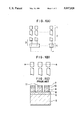
- FIGS. 1(A) to 1(C) An example of such prior art image sensors is illustrated in FIGS. 1(A) to 1(C) for fasilitating the understanding of the background of the present invention.
- the image sensor is a line sensor which is provided with a row of photosensitive regions.
- FIG. 1(A) is a plan view of an electrode arrangement. A number of electrode strips are formed in parallel together with head portions 1 located just above the underlying photosensitive regions. Each head portion is connected with a driving IC through a lead portion 2 and a contact 4 by means of wiring 3.
- FIG. 1(B) is an expanded view of the head portions of the electrode arrangement and FIG. 1(C) is a cross sectional view taken along a--a line of FIG. 1(B).
- the photosensitive region is comprised of a transparent common electrode 6 formed just on a glass substrate 5, a photosensitive semiconductor layer consisting of a p-layer 8, an i-layer 9 and an n-layer 10 and an opposed electrode layer 7 stacked in this order.
- the photosensitive semiconductor layer and the opposed electrode layer are divided into a row of photosensitive regions by grooves 11. The groove is provided for avoiding current leakage between adjacent photosensitive regions.
- the grooves 11 are formed by etching after deposition of the respective layers. During the etching process, however, the photosensitive regions are often damaged. The grooves 11 may receive some debris which may form bypass current paths between the layers.
- the formation of this grooves 11 is indispensable in order to avoid crosstalk between pixels because the ratio of the resistance of the layer 10 in a lateral direction to the resistance in the direction normal to the layered structure is only 10 or lower. The ratio can be increased by making use of amorphous silicon semiconductor to some extent. However, the ratio is not so low as to dispense with the formation of the grooves.
- the photosensitive semiconductor region consists of an n-type layer, an i-type layer and a p-type layer stacked in this order, and a pair of electrodes provided outside of the n-type and p-type layers for outputting.
- the n-type and p-type layers are made of the material of a high resistivity. Photo-created carriers are drifted by virtue of an electric field induced in the depletion layer across the i-type layer toward the outside regions of the n-type and p-type layers on which the pair of electrodes are formed.
- the high resistivity of the n-type and p-type layers functions to reduce undesirable currents passing across the pixels.
- the preferable materials suitable for the layer of a high resistivity are silicon nitride and silicon carbide.
- FIGS. 1(A) and 1(B) are plan and expanded views showing an electrode arrangement defining pixels of an image sensor.
- FIG. 1(C) is a cross sectional view showing a prior art image sensor.
- FIG. 2 is a cross sectional view showing an image sensor in accordance with an embodiment of the present invention.
- FIG. 3 is a cross sectional view showing an image sensor in accordance with another embodiment of the present invention.
- the sensor comprises a glass substrate 12, a plurality of transparent electrode strips 13 arranged in a row, an n-type amorphous silicon nitride semiconductor film 14, an intrinsic (i-type) amorphous silicon semiconductor film 15 and a p-type amorphous silicon nitride semiconductor film 16 and a aluminium common electrode 17.
- Each electrode strip 13 defines a photosensitive region with corresponding portions of the semiconductor films 14, 15 and 16 and the common electrode 17 overlying them.
- Three photosensitive regions are illustrated in FIG. 2.
- the geometry of the electrodes 13 may be equivalent to that illustrated in FIGS. 1(A) and 1(B).
- the resistances of the silicon nitride films 14 and 16 measured in a lateral direction parallel therewith were not less than 1 ⁇ 10 10 ohm.
- the ratios of the lateral resistances to the resistance normal to the film were not less than 100.
- FIG. 3 illustrates another embodiment in accordance with the present invention. This embodiment will be described by way of its manufacturng process. Chromium is deposited on a Corning #7059 glass substrate in order to form a common electrode 19 of 1000 ⁇ thickness. An n-type amorphous silicon carbide semiconductor film 20 is deposited on the common electrode 19 by plasma CVD using, as reactive gases, SiH 4 , CH 4 and PH 4 to a thickness of 300 ⁇ . An i-type amorphous silicon semiconductor film 21 is deposited on the n-type semiconductor film by plasma CVD using SiH 4 to a thickness of 1 micron.
- a p-type amorphous silicon carbide semiconductor film 22 is deposited to a thickness of 300 ⁇ by plasma CVD using SiH 4 , CH 4 and BH 4 .
- electrode strips 23 made of a transparent conductive material such as indium tin oxide are formed on the p-type film to a thickness of 1500 ⁇ in order to define photosensitive regions of photodiode structure.
- the reactive gases employed for embodying the present invention may be, as the silicon source SiH 4 , Si 2 H 6 or Si 3 H 8 , as the carbon source CH 4 , C 2 H 2 , C 2 H 4 or C 2 H 6 , as the nitrogen source N 2 or NH 3 , as the dopant gas PH 3 or B 2 H 6 .
- Each reactive gas is introduced together with a carrier gas such as He or H 2 .
- the photosensitivity of the image sensor was increased by about 30% because the photosensitive structure was not damaged during the manufacturing process.
- the photosensitive semiconductor films can be formed with pin, nip, ip, np, pi or ni junctions.
Landscapes
- Solid State Image Pick-Up Elements (AREA)
- Transforming Light Signals Into Electric Signals (AREA)
- Light Receiving Elements (AREA)
Abstract
Description
Claims (6)
Applications Claiming Priority (2)
| Application Number | Priority Date | Filing Date | Title |
|---|---|---|---|
| JP63-107958 | 1988-04-30 | ||
| JP63107958A JPH01278774A (en) | 1988-04-30 | 1988-04-30 | Image sensor |
Publications (1)
| Publication Number | Publication Date |
|---|---|
| US5017828A true US5017828A (en) | 1991-05-21 |
Family
ID=14472375
Family Applications (1)
| Application Number | Title | Priority Date | Filing Date |
|---|---|---|---|
| US07/342,857 Expired - Lifetime US5017828A (en) | 1988-04-30 | 1989-04-25 | Image sensor |
Country Status (2)
| Country | Link |
|---|---|
| US (1) | US5017828A (en) |
| JP (1) | JPH01278774A (en) |
Cited By (1)
| Publication number | Priority date | Publication date | Assignee | Title |
|---|---|---|---|---|
| EP0755081A1 (en) * | 1995-07-21 | 1997-01-22 | Commissariat A L'energie Atomique | Photosensitive structure resistant to hard electromagnetic radiations and its use in video cameras |
Citations (2)
| Publication number | Priority date | Publication date | Assignee | Title |
|---|---|---|---|---|
| US4754152A (en) * | 1985-06-24 | 1988-06-28 | Mitsubishi Denki Kabushiki Kaisha | Optical reader and method for its manufacture |
| US4868623A (en) * | 1984-11-27 | 1989-09-19 | Fuji Electric Co., Ltd. | Image sensing device |
Family Cites Families (1)
| Publication number | Priority date | Publication date | Assignee | Title |
|---|---|---|---|---|
| JPS6421958A (en) * | 1987-07-16 | 1989-01-25 | Toppan Printing Co Ltd | Image sensor |
-
1988
- 1988-04-30 JP JP63107958A patent/JPH01278774A/en active Pending
-
1989
- 1989-04-25 US US07/342,857 patent/US5017828A/en not_active Expired - Lifetime
Patent Citations (2)
| Publication number | Priority date | Publication date | Assignee | Title |
|---|---|---|---|---|
| US4868623A (en) * | 1984-11-27 | 1989-09-19 | Fuji Electric Co., Ltd. | Image sensing device |
| US4754152A (en) * | 1985-06-24 | 1988-06-28 | Mitsubishi Denki Kabushiki Kaisha | Optical reader and method for its manufacture |
Cited By (3)
| Publication number | Priority date | Publication date | Assignee | Title |
|---|---|---|---|---|
| EP0755081A1 (en) * | 1995-07-21 | 1997-01-22 | Commissariat A L'energie Atomique | Photosensitive structure resistant to hard electromagnetic radiations and its use in video cameras |
| FR2737045A1 (en) * | 1995-07-21 | 1997-01-24 | Commissariat Energie Atomique | PHOTOSENSITIVE STRUCTURE HARDENED TO HARD ELECTROMAGNETIC RADIATION AND ITS APPLICATION TO VIDEO CAMERAS |
| US5844292A (en) * | 1995-07-21 | 1998-12-01 | Commissariat A L'energie Atomique | Photosensitive structure hardened to hard electromagnetic radiation and its application to video cameras |
Also Published As
| Publication number | Publication date |
|---|---|
| JPH01278774A (en) | 1989-11-09 |
Similar Documents
| Publication | Publication Date | Title |
|---|---|---|
| US5481124A (en) | Laminated solid-state image pickup device | |
| US6281561B1 (en) | Multicolor-color sensor | |
| EP0809298A1 (en) | Solid-state image pickup device | |
| US4405915A (en) | Photoelectric transducing element | |
| US6018169A (en) | Solid-state image sensor and method of fabricating the same | |
| EP0362928B1 (en) | Display arrangement provided with diodes and method of manufacturing the display arrangement | |
| US20100193848A1 (en) | Image sensor of stacked layer structure and manufacturing method thereof | |
| US4999693A (en) | Photoelectric conversion device with a high response speed | |
| EP0428050B1 (en) | Photosensor having an amorphous silicon photoabsorption layer | |
| JPH0456468B2 (en) | ||
| US5017828A (en) | Image sensor | |
| US4868623A (en) | Image sensing device | |
| US4141024A (en) | Solid state image sensing device | |
| JP2777663B2 (en) | Contact type linear image sensor | |
| US4394675A (en) | Transparent asymmetric electrode structure for charge coupled device image sensor | |
| US4546243A (en) | Elongated light receiving element assembly | |
| US5014100A (en) | Image sensor free from undesirable incident light rays which have not been reflected in the surface bearing the image to be sensed | |
| KR960007482B1 (en) | Layer-built solid state image sensing device | |
| JPH05110056A (en) | Image sensor | |
| JPS6322465B2 (en) | ||
| JPS61251068A (en) | Solid-state image pickup device | |
| JPH01107580A (en) | Photodetector and manufacture thereof | |
| JPH05347427A (en) | Photosensor | |
| JPS6148797B2 (en) | ||
| JPH0521777A (en) | Reading device and manufacturing method thereof |
Legal Events
| Date | Code | Title | Description |
|---|---|---|---|
| AS | Assignment |
Owner name: SEMICONDUCTOR ENERGY LABORATORY CO., LTD., A CORP. Free format text: ASSIGNMENT OF ASSIGNORS INTEREST.;ASSIGNORS:FUKADA, TAKESHI;SAKAMA, MITSUNORI;AMACHI, NOBUMITSU;AND OTHERS;REEL/FRAME:005066/0951 Effective date: 19890419 |
|
| STCF | Information on status: patent grant |
Free format text: PATENTED CASE |
|
| FEPP | Fee payment procedure |
Free format text: PAYOR NUMBER ASSIGNED (ORIGINAL EVENT CODE: ASPN); ENTITY STATUS OF PATENT OWNER: LARGE ENTITY |
|
| FPAY | Fee payment |
Year of fee payment: 4 |
|
| FPAY | Fee payment |
Year of fee payment: 8 |
|
| FEPP | Fee payment procedure |
Free format text: PAYER NUMBER DE-ASSIGNED (ORIGINAL EVENT CODE: RMPN); ENTITY STATUS OF PATENT OWNER: LARGE ENTITY Free format text: PAYOR NUMBER ASSIGNED (ORIGINAL EVENT CODE: ASPN); ENTITY STATUS OF PATENT OWNER: LARGE ENTITY |
|
| FPAY | Fee payment |
Year of fee payment: 12 |