US4989136A - Delay management method and device - Google Patents
Delay management method and device Download PDFInfo
- Publication number
- US4989136A US4989136A US07/056,475 US5647587A US4989136A US 4989136 A US4989136 A US 4989136A US 5647587 A US5647587 A US 5647587A US 4989136 A US4989136 A US 4989136A
- Authority
- US
- United States
- Prior art keywords
- address
- token
- delay
- memory
- section
- Prior art date
- Legal status (The legal status is an assumption and is not a legal conclusion. Google has not performed a legal analysis and makes no representation as to the accuracy of the status listed.)
- Expired - Fee Related
Links
Images


Classifications
-
- G—PHYSICS
- G06—COMPUTING OR CALCULATING; COUNTING
- G06F—ELECTRIC DIGITAL DATA PROCESSING
- G06F13/00—Interconnection of, or transfer of information or other signals between, memories, input/output devices or central processing units
- G06F13/14—Handling requests for interconnection or transfer
- G06F13/16—Handling requests for interconnection or transfer for access to memory bus
- G06F13/1668—Details of memory controller
- G06F13/1689—Synchronisation and timing concerns
-
- G—PHYSICS
- G06—COMPUTING OR CALCULATING; COUNTING
- G06F—ELECTRIC DIGITAL DATA PROCESSING
- G06F12/00—Accessing, addressing or allocating within memory systems or architectures
- G06F12/02—Addressing or allocation; Relocation
- G06F12/0223—User address space allocation, e.g. contiguous or non contiguous base addressing
- G06F12/023—Free address space management
-
- G—PHYSICS
- G06—COMPUTING OR CALCULATING; COUNTING
- G06F—ELECTRIC DIGITAL DATA PROCESSING
- G06F9/00—Arrangements for program control, e.g. control units
- G06F9/06—Arrangements for program control, e.g. control units using stored programs, i.e. using an internal store of processing equipment to receive or retain programs
- G06F9/30—Arrangements for executing machine instructions, e.g. instruction decode
- G06F9/38—Concurrent instruction execution, e.g. pipeline or look ahead
- G06F9/3824—Operand accessing
Definitions
- the present invention relates to a delay management method and device which in an electronic computer enables read requests relating to data not yet stored in the computer memory to be delayed.
- an electronic computer such as a microcomputer
- a read request is made which indicates the specific memory addresses in which the data is stored.
- the stored data is then read out and processed as required.
- serial processing computers in which program commands are executed in individual independent devices, there are times when read requests are made which relate to data which has not yet reached the memory, and it is necessary to have a mechanism whereby the read request is delayed until the required data has reached the memory.
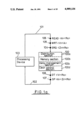
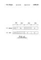
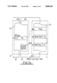
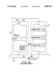
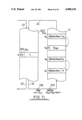
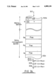
- FIGS. 1a and 1b schematically illustrate a system incorporating such a delay management device, the system comprising a processing device and a memory device which has a facility to delay read requests (hereinafter referred to simply as a "read delay device").
- a read delay device 100 is illustrated in FIG. 1a, the read delay device comprising a distribution (allocation) section 100a, a memory section 100b, a delay (defer) management section 100c and a clear control section 100d.
- Channels 101 and 102 are provided for sending information from processing device 103 to the read delay device 100 and from the read delay device 100 to the processing device 103 respectively.
- the exchange of information between the processing device 103 and the read delay device 100 comprises the sending of a single data packet (herein referred to as a "token").
- SRQ space request
- SP space provided
- the memory section 100b also receives a write (WRT) token 105 and a read request (READ) token 106, in response to the former it enters a parameter V into an address A, and in response to the latter it reads the contents V of address A and sends the read data to the processing device 103 in the form of a data (DT) token 108.
- the significance of the data sent back is indicated by parameter Ra.
- Delay management section 100c and clear control section 100d do not communicate tokens directly to the processing device 103.
- Delay management section 100c manages read request tokens which relate to data which has not yet arrived in the memory section 100b, and clear control section 100 d clears memory areas which are no longer required. Each token is distinguished from the others by a code which forms a part of that token.
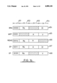
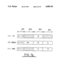
- FIG. 1b shows the form of each token.
- the token forms identified by numerals 464 to 468 correspond to tokens 104 to 108 respectively in FIG. 1a.
- each token comprises four fields, namely a first code field 451, a second code field 452, a third code field 453, and a fourth code field 454.
- Code field 451 serves the purpose of distinguishing between the different kinds of tokens.
- field 451 is allotted four bits, which can designate sixteen different kinds of token.
- the second, third and fourth fields 452 to 454 each have twenty four bits, but any number of bits can be allocated to each field depending on the requirements of the system.
- the shaded parts of the diagrams show fields which are not used in the tokens to which the diagrams relate.
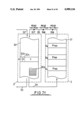
- FIGS. 2a, 2b and 2c serve to explain in detail the workings of memory section 100b and the delay management section 100c.
- numeral 100b denotes the memory section
- 201 and 202 are the entry and exit channels respectively of tokens going in and out of memory section 100b.
- the words inside memory section 100b contain a "flag field” and a "data field”.
- the flag field of address A comprises a valid flag (P) 203 which shows whether or not there is any significant data in the data field and delay flag (D) 204 which shows whether or not a read request delay has occurred. That is to say when an entry has been made in the data field by the entry of data, the token valid flag 203 becomes "1", and when this entry is cancelled, the flag 203 becomes "0".
- delay flag 204 becomes "1".
- the action of memory section 100b depends upon the condition of the valid flag in address A.
- the read request token is stored in the field 207 (for example address Q) at the discretion of the delay management section 100c.
- the read address parameter A is deleted and stored, but this deletion is in practice essentially not necessary.
- the information which shows that there is a first delay token in address A is shown in a linking field 208.
- the read request token store address pointer Q is stored. "1" is entered in the delay flag 204.
- the data V is entered in the data field of address A, and at the same time "1" is entered in valid flag 303 and "0" is entered in delay flag 304.
- the data V which is being entered in each address in the delay chain are correlated and data tokens 308 to 310 are formed and sent to the processing device.
- the addresses Q1 to Q3 which previously were used to store the delay tokens become free and can be used during subsequent delay processing.
- Numerals 401 to 404 in FIGS. 4a to 4e correspond to numerals 301 to 304 in FIGS. 3a and 3b, and indicate corresponding functions.
- Channels 409 and 410 carry tokens going from delay management section 100c to memory section 100b and from memory section 100b to delay management section 100c respectively.
- FIG. 4a two read request tokens are shown as having been previously delayed.
- a further read request token 411 then arrives related to address A. In these circumstances the action of each part of the system is as described hereinbelow:
- the token 412 when the delay token 412 arrives at delay management device 100c, the token 412 is housed in an appropriate free address (for example Q3), and at the same time a new leading address token (NQA) 413 is output to memory device 100b.
- the token 413 has the purpose of delivering the new leading address Q3 of the series of delay tokens to the memory device 100b.
- FIG. 4f The new tokens DREAD and NQA which have appeared as described above are shown in FIG. 4f.
- Fields 751 to 754 in FIG. 4f correspond to fields 451 to 454 in FIG. 1b.
- the shaded sections of the diagram are fields which are not used.
- token 413 arrives at memory section 100b at the same time as a new read request token 414 related to address A.
- token 413 arrives after token 414, then referring to FIG. 4e, token 414 is delayed and becomes token 411, and the parameter of delayed token 411 becomes the above new value Q2. Even if the token 411 is stored in delay management section 100c, two tokens are associated with the address Q2, and the delay tokens do not therefore form the normal series of single tokens.
- a delay management method for delaying read request instructions which relate to data not yet stored in a memory section of a computer, wherein a delay management section of the computer sends to the memory section data identifying free addresses within the delay management section, the free address data is stored in the memory section, the memory section detects when a read request is received relating to an address of the memory section to which data has not yet been written, when such a read request is detected the memory section sends data to the delay management section identifying the read request to be delayed and a free address taken from the addresses stored in the memory section, the free address sent to the delay management section is cancelled from the addresses stored in the memory section, the delay management section stores the read request data received from the memory section at the free address identified by the received data, when data is written to the address of the memory section to which the delayed read request relates, a release request is sent by the memory section to the delay management section, the delay management section responds to the release request sending the delayed read request to the memory section, and the delay management section sends data
- the invention also provides a delay management device for delaying read request instructions which relates to data not yet stored in a memory section of a computer, comprising management section, means for identifying free addresses in the delay management section, means for communicating free addresses from the delay management section to the memory section, means in the memory section for storing data identifying the free addresses, means for detecting a read request to be delayed which relates to an address of the memory section to which data has not yet been written, means for sending data to the delay management section identifying a detected read request which is to be delayed and a selected free address taken from the free address storing means, means for cancelling the selected free address from the free address storing means, means for storing the read request received from the memory section at the selected free address of the delay management section, means for detecting the writing of data to the said address of the memory section, means for generating a release request when the writing of data to the said address is detected, means for communicating the release request to the delay management section, means responsive to the release request to generate the delayed read request, means for communicating the generated delayed read
- the object of the present invention is, when a read request is made for data which has not yet arrived in the memory device, the memory device sends to the delay management section not only free address information which has previously been received from the delay management section, but also data relating to the read request which is to be delayed, the delay management section storing the read request data in the free address identified by the information sent with the read request data.
- FIG. 1a is a block diagram of a prior art delay management device
- FIG. 1b is a schematic diagram illustrating the form of tokens used in the device of FIG. 1a;
- FIGS. 2a to 2c, 3a and 3b, and 4a to 4f are schematic diagrams illustrating the operation of the prior art delay management device
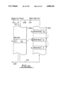
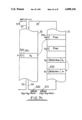
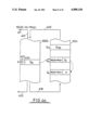
- FIG. 5 is a block diagram of a delay management device embodying the present invention.
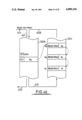
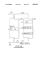
- FIG. 6 is a block diagram illustrating elements of the device of FIG. 1;
- FIGS. 7a to 7j are schematic diagrams illustrating the operation of a delay management device embodying the invention.
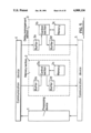
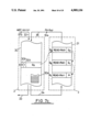
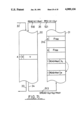
- numeral 1 designates a processing device, which corresponds to the processing device 103 of FIG. 1.
- Numerals 2 and 3 denote a memory section and a delay management section which correspond to the memory section 100b and the delay management section 100c of FIG. 1 respectively.
- Numerals 4 and 5 are communications devices which collect and deliver tokens which are passed between the operating device 1, the memory section 2, and the delay management section 3, and correspond to channels 101 and 102 of FIG. 1.
- the memory section 2 comprises a buffer 2a which maintains temporarily tokens which are received from communications device 4.
- a control section 2b is provided in which the nature of received tokens is analysed and, depending on the type of token received, either stores the token parameters in memory 2c, or reads out the contents of memory 2c.
- a buffer 2d serves the purpose of sending tokens which emanate from control section 2b to the communications device 5.
- a buffer 3a temporarily stores tokens received from communications device 4.
- a control section 3b analyses tokens received and, depending on their type, either stores their parameters in a memory 3c or reads the contents of the memory 3c.
- a buffer 3d sends to the communications device 5 tokens which emanate from the control section 3b.
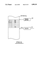
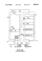
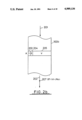
- FIG. 6 shows a part of the space in the memory 2c.
- the free addresses in memory 3c for example Q3, Q4, Q5» Qn.
- the free address space of memory 3c is identified by stack pointer 20.
- a buffer 21 communicates the address Qn+1 of a free address space of memory 3c which has been released by the delay management device 3, and these free addresses are accumulated.
- FIGS. 5 and 6 just show an outline of one example of the present invention, and the present invention is not limited for example to the buffer 2a and 2d and the control section 2b in the memory section 2.
- the essence of the present invention can more easily be understood by explaining the workings of the invention with reference to FIGS. 7a to 7j.
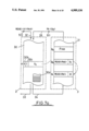
- numeral 30 represents memory space in the memory 2c of memory section 2
- 30a represents a memory section in which the free address space of memory 3c (shown in FIG. 6) is stored.
- Numerals 30b and 30c represent valid and delay flags which correspond to those shown in FIG. 2a
- numeral 31 represents a memory space in the memory 3c of delay management device 3.
- Numerals 32, 33, 34 and 35 identify channels along which tokens are sent, and they correspond to the collection and delivery devices 4 and 5 of FIG. 5.
- a token (FA) 511 is sent containing a free address available in delay management section 3, and stored in the memory section 30a of the memory section 2. So the free address token 511 carries the free address in delay management section 3 as a parameter and stores it in address housing section 30a.
- Q4 is the free address which is available within the delay management section 3, and is stored in the address section 30a in the memory 2.
- data is stored at address Q4.
- FIGS. 7e and 7f when a write token WRT which relates to address A arrives, the delay token or tokens which relate to address A are released, and the procedure is as described hereinbelow.
- the memory 2 When the memory 2 receives the write token, it looks at delay flag 30c, and because the value of this is "1" it determines that the address (in delay management section 3) of a delay token is stored in address A. As a result, at the same time as entering the data V to address A, the release request (RRQ) token 516 is generated. Then, when the existing flag 30b is "1", the delay flag 30c is set to "0".
- the release request (RRQ) token 516 has address A and the address Q3 housed therein as its parameters, and it is sent to delay management section 3.
- the delay management section 3 When the delay management section 3 receives the release request token 516, it recognises from the parameter Q3 the first of the series of delay tokens which should be released, and from the parameter A the address to which the tokens to be released relate. As a result the series of read tokens 517 to 519 is generated and sent to the memory section 2. Then each of the addresses in which the delay tokens have been stored in the delay management section 3 becomes a free address.
- memory section 2 When memory section 2 receives the tokens 517 to 519, it reads data from the address A and sends the read data V in a data token to the operation device.
- FIGS. 7a to 7f Examples of the form of the tokens DREAD, FA and RRQ as used in FIGS. 7a to 7f are shown in FIG. 7g (the shaded section of the drawing are fields which are not used).
- 551 to 554 correspond to 451 to 454 respectively, in FIG. 1b.
- DREAD in FIG. 7g is not the same as it is in FIG. 4f; one more field is used.
- FA corresponds to NQA in FIG. 4f except that one less field is used.
- free address token 511 has arrived in the address store section 30a of the memory section 2 at the same time as the read request token 512, and it is all right for more than one free address token to accumulate in the store section 30a of the memory section 2.
- the situation can arise in which tokens overtake each other in the token channels 32, 33, 34 and 35.
- 31a is a valid flag which is associated with each address in the delay processing section 30. The purpose of the flag 31a is to show if the address holds a delay token, or if it is free.
- two delay tokens 513 and 520 are in the channel 34 and there is a write token 515 in the channel 32.
- the memory section 2 receives the write token 515, and processes it.
- the delay token 520 overtakes the delay token 513, and arrives at the delay processing section 3 first and is processed. The result of this is as shown in FIG. 7i.
- a "1" is entered in valid flag 31a of address Q4.
- the memory section 2 then receives the write token 515, and investigates the address A. Since there is a token which has been delayed with relation to this address, a release token 516 is generated.
- the release token 516 comprises as parameters the address A and the delay address Q4 which has been held in address A. Furthermore, the value V is entered in the address A.
- the delay token 520 has arrived in the delay processing section 3, and the parameters Q3 and Ra4 have been stored in the delay address Q4, so that the series field of the address Q4 indicates the free address Q3, the address Q3 is still free as the token 513 has not yet been received. Thus, if one delay token overtakes another, the series can be broken.
- the release request token 516 may overtake the delay token 513, and when it has arrived at the delay processing section 3, it prompts the release of the broken delay series.
- the action of the delay section 3 to deal with such circumstances is as follows:
- the delay processing section 3 reads the address Q4, which indicates the delay address parameter held in the release request token 516, and since the valid flag in this is "1" it joins the address parameter A in the memory section 2 to the parameter Ra4 which it holds, reverts the read request token back to its original state, and sends it out as the read token 518 of FIG. 7j.
- the delay address Q3 which is identified by the series field of the delay address Q4, and reviews the valid flag of address Q3. Since this flag is "0" and therefore the data necessary to generate a Read token is not yet available in address Q3, a new release request token RRQ is generated which has the release address parameter Q3, and is sent out as a release request token 521 as shown in FIG. 3j.
- the release request token 521 passes through the memory section 2 without undergoing any processing, and is passed via channel 34 back to the delay processing section 3. If in this time the delay token 513 has arrived at the delay processing section 3, it is stored at address Q3 to complete the series, and all the delay tokens of the series are then released. If the second release request token 521 overtakes the delay token 513, the delay processing section 3 makes another release request token which has the same parameters as the release requirement token 521. Whatever happens, until the delay token 513 arrives in the delay processing section 3 and is processed, the above release request process is repeated, until finally all the tokens in the series are released.
- the delay processing section 3 when the delay processing section 3 receives a release request token, it reads the delay address of that token, and then proceeds as follows:
- the delay processing section joins the memory section address parameter held by the release request token to the parameter held by the address, and generates a read request token READ identical to the token which was originally delayed.
- the generated read request is sent out, and then the delay processing section read the address which is identified by the series field of that address, and follows the procedure (a) above for that address.
- the delay processing section generates a new release request token including the address which has the valid flag "0" as the delay address parameter.
- the generated release request is then recirculated until the valid flag contains "1".
- the read request when a read request relating to data which has not yet been received by a memory device is attempted, the read request is delayed and information which is essential for carrying out this read request is stored in a delay management device.
- the invention is constructed so that the read request can then be carried out. Therefore the above-mentioned memory device and delay management device can be distinguished from each other, and even in situations where communication between the two is only done by token packets, the two devices can operate without problems arising.
- the free addresses of the above-mentioned delay management device are allowed to accumulate in the above-mentioned memory device.
- a free address at which a delay token is to be stored is stored in the address to be read.
- the delay token is then sent to the delay management device, the delay token including the free address token from the store in the memory device.
Landscapes
- Engineering & Computer Science (AREA)
- Theoretical Computer Science (AREA)
- Physics & Mathematics (AREA)
- General Engineering & Computer Science (AREA)
- General Physics & Mathematics (AREA)
- Software Systems (AREA)
- Memory System (AREA)
- Communication Control (AREA)
- Data Exchanges In Wide-Area Networks (AREA)
Applications Claiming Priority (2)
| Application Number | Priority Date | Filing Date | Title |
|---|---|---|---|
| GB8613068 | 1986-05-29 | ||
| GB868613068A GB8613068D0 (en) | 1986-05-29 | 1986-05-29 | Delay management |
Publications (1)
| Publication Number | Publication Date |
|---|---|
| US4989136A true US4989136A (en) | 1991-01-29 |
Family
ID=10598627
Family Applications (1)
| Application Number | Title | Priority Date | Filing Date |
|---|---|---|---|
| US07/056,475 Expired - Fee Related US4989136A (en) | 1986-05-29 | 1987-05-28 | Delay management method and device |
Country Status (5)
| Country | Link |
|---|---|
| US (1) | US4989136A (de) |
| EP (1) | EP0249344B1 (de) |
| JP (2) | JPS63233436A (de) |
| DE (1) | DE3787213T2 (de) |
| GB (1) | GB8613068D0 (de) |
Cited By (4)
| Publication number | Priority date | Publication date | Assignee | Title |
|---|---|---|---|---|
| US5408602A (en) * | 1990-07-31 | 1995-04-18 | Giokas; Dennis G. | System and method for emulating a window management environment having a uniform windowing interface |
| US20060106971A1 (en) * | 2004-11-18 | 2006-05-18 | International Business Machines (Ibm) Corporation | Management of metadata in a storage subsystem |
| US20060106829A1 (en) * | 2004-11-18 | 2006-05-18 | International Business Machines (Ibm) Corporation | Clearing metadata tracks in a storage system |
| US20060106891A1 (en) * | 2004-11-18 | 2006-05-18 | International Business Machines (Ibm) Corporation | Managing atomic updates on metadata tracks in a storage system |
Families Citing this family (1)
| Publication number | Priority date | Publication date | Assignee | Title |
|---|---|---|---|---|
| EP0495167A3 (en) * | 1991-01-16 | 1996-03-06 | Ibm | Multiple asynchronous request handling |
Citations (4)
| Publication number | Priority date | Publication date | Assignee | Title |
|---|---|---|---|---|
| US3736566A (en) * | 1971-08-18 | 1973-05-29 | Ibm | Central processing unit with hardware controlled checkpoint and retry facilities |
| US4149245A (en) * | 1977-06-09 | 1979-04-10 | International Business Machines Corporation | High speed store request processing control |
| US4385365A (en) * | 1978-02-13 | 1983-05-24 | Hitachi, Ltd. | Data shunting and recovering device |
| US4426681A (en) * | 1980-01-22 | 1984-01-17 | Cii Honeywell Bull | Process and device for managing the conflicts raised by multiple access to same cache memory of a digital data processing system having plural processors, each having a cache memory |
Family Cites Families (2)
| Publication number | Priority date | Publication date | Assignee | Title |
|---|---|---|---|---|
| US3588829A (en) * | 1968-11-14 | 1971-06-28 | Ibm | Integrated memory system with block transfer to a buffer store |
| GB8401804D0 (en) * | 1984-01-24 | 1984-02-29 | Int Computers Ltd | Data storage apparatus |
-
1986
- 1986-05-29 GB GB868613068A patent/GB8613068D0/en active Pending
-
1987
- 1987-05-15 EP EP87304320A patent/EP0249344B1/de not_active Expired - Lifetime
- 1987-05-15 DE DE87304320T patent/DE3787213T2/de not_active Expired - Fee Related
- 1987-05-28 US US07/056,475 patent/US4989136A/en not_active Expired - Fee Related
- 1987-05-28 JP JP62132567A patent/JPS63233436A/ja active Pending
- 1987-05-28 JP JP62132566A patent/JPS63233435A/ja active Pending
Patent Citations (4)
| Publication number | Priority date | Publication date | Assignee | Title |
|---|---|---|---|---|
| US3736566A (en) * | 1971-08-18 | 1973-05-29 | Ibm | Central processing unit with hardware controlled checkpoint and retry facilities |
| US4149245A (en) * | 1977-06-09 | 1979-04-10 | International Business Machines Corporation | High speed store request processing control |
| US4385365A (en) * | 1978-02-13 | 1983-05-24 | Hitachi, Ltd. | Data shunting and recovering device |
| US4426681A (en) * | 1980-01-22 | 1984-01-17 | Cii Honeywell Bull | Process and device for managing the conflicts raised by multiple access to same cache memory of a digital data processing system having plural processors, each having a cache memory |
Cited By (7)
| Publication number | Priority date | Publication date | Assignee | Title |
|---|---|---|---|---|
| US5408602A (en) * | 1990-07-31 | 1995-04-18 | Giokas; Dennis G. | System and method for emulating a window management environment having a uniform windowing interface |
| US20060106971A1 (en) * | 2004-11-18 | 2006-05-18 | International Business Machines (Ibm) Corporation | Management of metadata in a storage subsystem |
| US20060106829A1 (en) * | 2004-11-18 | 2006-05-18 | International Business Machines (Ibm) Corporation | Clearing metadata tracks in a storage system |
| US20060106891A1 (en) * | 2004-11-18 | 2006-05-18 | International Business Machines (Ibm) Corporation | Managing atomic updates on metadata tracks in a storage system |
| US7885921B2 (en) | 2004-11-18 | 2011-02-08 | International Business Machines Corporation | Managing atomic updates on metadata tracks in a storage system |
| US8676748B2 (en) | 2004-11-18 | 2014-03-18 | International Business Machines Corporation | Clearing metadata tracks in a storage system |
| US8856467B2 (en) | 2004-11-18 | 2014-10-07 | International Business Machines Corporation | Management of metadata in a storage subsystem |
Also Published As
| Publication number | Publication date |
|---|---|
| EP0249344B1 (de) | 1993-09-01 |
| DE3787213T2 (de) | 1994-01-13 |
| DE3787213D1 (de) | 1993-10-07 |
| GB8613068D0 (en) | 1986-07-02 |
| EP0249344A3 (en) | 1989-09-06 |
| JPS63233435A (ja) | 1988-09-29 |
| EP0249344A2 (de) | 1987-12-16 |
| JPS63233436A (ja) | 1988-09-29 |
Similar Documents
| Publication | Publication Date | Title |
|---|---|---|
| US5025367A (en) | Storage allocation and garbage collection using liberate space tokens | |
| EP0191036B1 (de) | Datenbanksicherstellungsverfahren | |
| US6038592A (en) | Method and device of multicasting data in a communications system | |
| US5155858A (en) | Twin-threshold load-sharing system with each processor in a multiprocessor ring adjusting its own assigned task list based on workload threshold | |
| US4864495A (en) | Apparatus for controlling vacant areas in buffer memory in a pocket transmission system | |
| EP0553560A2 (de) | Kommunikationssystem | |
| DE3853162T2 (de) | Gemeinsamer intelligenter Speicher für die gegenseitige Verbindung von verteilten Mikroprozessoren. | |
| EP0407087B1 (de) | Eingabewarteschlange für Speichersubsysteme | |
| EP0366344B1 (de) | Multiprozessor-Belastungsteilungsanordnung | |
| US4989136A (en) | Delay management method and device | |
| US6629221B2 (en) | Memory management system for enabling writing of data blocks by substitution and preventing premature elimination of data blocks | |
| US5113502A (en) | Method and apparatus for saving and performing industrial control commands | |
| JPH0318398B2 (de) | ||
| AU771174B2 (en) | Method and system for transmitting a chain of messages for database | |
| US4860250A (en) | Data packet shortening method and device | |
| EP0569120B1 (de) | Datenpuffersystem | |
| US6181701B1 (en) | Method for optimizing the transmission of ATM cells via connection sections | |
| US6570882B1 (en) | Method of managing a queue of digital cells | |
| US6822941B1 (en) | Method and network element for relaying event messages | |
| JPH02122365A (ja) | プロセッサ割当て方式 | |
| JPH0230534B2 (de) | ||
| EP0994607A1 (de) | Verfahren und Einrichtung zur ATM-Verkehrsformung | |
| EP0609714A1 (de) | Datensammlungssystem vom Abfragetyp | |
| CN1138905A (zh) | 根据有限自动装置的原理进行技术过程控制的方法 | |
| JPH06301708A (ja) | 取引情報配信装置 |
Legal Events
| Date | Code | Title | Description |
|---|---|---|---|
| AS | Assignment |
Owner name: MATSUSHITA ELECTRIC INDUSTRIAL CO. LTD.,JAPAN Free format text: ASSIGNMENT OF ASSIGNORS INTEREST;ASSIGNORS:GURD, JOHN R.;KAWAKAMI, KATSURA;SIGNING DATES FROM 19880219 TO 19880301;REEL/FRAME:004864/0437 Owner name: VICTORIA UNIVERSITY OF MANCHESTER, THE,UNITED KING Free format text: ASSIGNMENT OF ASSIGNORS INTEREST;ASSIGNORS:GURD, JOHN R.;KAWAKAMI, KATSURA;SIGNING DATES FROM 19880219 TO 19880301;REEL/FRAME:004864/0437 Owner name: VICTORIA UNIVERSITY OF MANCHESTER, THE, OXFORD ROA Free format text: ASSIGNMENT OF ASSIGNORS INTEREST.;ASSIGNORS:GURD, JOHN R.;KAWAKAMI, KATSURA;REEL/FRAME:004864/0437;SIGNING DATES FROM 19880219 TO 19880301 Owner name: MATSUSHITA ELECTRIC INDUSTRIAL CO. LTD., 1006 OHAZ Free format text: ASSIGNMENT OF ASSIGNORS INTEREST.;ASSIGNORS:GURD, JOHN R.;KAWAKAMI, KATSURA;REEL/FRAME:004864/0437;SIGNING DATES FROM 19880219 TO 19880301 |
|
| FEPP | Fee payment procedure |
Free format text: PAYOR NUMBER ASSIGNED (ORIGINAL EVENT CODE: ASPN); ENTITY STATUS OF PATENT OWNER: LARGE ENTITY |
|
| REMI | Maintenance fee reminder mailed | ||
| LAPS | Lapse for failure to pay maintenance fees | ||
| FP | Lapsed due to failure to pay maintenance fee |
Effective date: 19950202 |
|
| STCH | Information on status: patent discontinuation |
Free format text: PATENT EXPIRED DUE TO NONPAYMENT OF MAINTENANCE FEES UNDER 37 CFR 1.362 |