US4979142A - Two-bit floating point divide circuit with single carry-save adder - Google Patents
Two-bit floating point divide circuit with single carry-save adder Download PDFInfo
- Publication number
- US4979142A US4979142A US07/339,261 US33926189A US4979142A US 4979142 A US4979142 A US 4979142A US 33926189 A US33926189 A US 33926189A US 4979142 A US4979142 A US 4979142A
- Authority
- US
- United States
- Prior art keywords
- divisor
- register
- dividend
- circuit
- adder circuit
- Prior art date
- Legal status (The legal status is an assumption and is not a legal conclusion. Google has not performed a legal analysis and makes no representation as to the accuracy of the status listed.)
- Expired - Fee Related
Links
Images
Classifications
-
- G—PHYSICS
- G06—COMPUTING OR CALCULATING; COUNTING
- G06F—ELECTRIC DIGITAL DATA PROCESSING
- G06F7/00—Methods or arrangements for processing data by operating upon the order or content of the data handled
- G06F7/38—Methods or arrangements for performing computations using exclusively denominational number representation, e.g. using binary, ternary, decimal representation
- G06F7/48—Methods or arrangements for performing computations using exclusively denominational number representation, e.g. using binary, ternary, decimal representation using non-contact-making devices, e.g. tube, solid state device; using unspecified devices
- G06F7/52—Multiplying; Dividing
- G06F7/535—Dividing only
-
- G—PHYSICS
- G06—COMPUTING OR CALCULATING; COUNTING
- G06F—ELECTRIC DIGITAL DATA PROCESSING
- G06F2207/00—Indexing scheme relating to methods or arrangements for processing data by operating upon the order or content of the data handled
- G06F2207/535—Indexing scheme relating to groups G06F7/535 - G06F7/5375
- G06F2207/5352—Non-restoring division not covered by G06F7/5375
-
- G—PHYSICS
- G06—COMPUTING OR CALCULATING; COUNTING
- G06F—ELECTRIC DIGITAL DATA PROCESSING
- G06F7/00—Methods or arrangements for processing data by operating upon the order or content of the data handled
- G06F7/38—Methods or arrangements for performing computations using exclusively denominational number representation, e.g. using binary, ternary, decimal representation
- G06F7/48—Methods or arrangements for performing computations using exclusively denominational number representation, e.g. using binary, ternary, decimal representation using non-contact-making devices, e.g. tube, solid state device; using unspecified devices
- G06F7/483—Computations with numbers represented by a non-linear combination of denominational numbers, e.g. rational numbers, logarithmic number system or floating-point numbers
- G06F7/487—Multiplying; Dividing
- G06F7/4873—Dividing
Definitions
- the present invention relates to a method and apparatus for performing certain floating point arithmetic operations in a data processing system. More particularly, the invention relates to an apparatus and method for implementing the apparatus, wherein five multiples of the divisor are produced without additional registers, for use in the divide iterations to produce a quotient, and wherein the floating point division circuit has a single carry-save adder circuit.
- the typical floating point arithmetic operation may be accomplished in either single precision or double precision format.
- Each of these formats utilizes a sign, exponent and fraction field, where the respective fields occupy predefined portions of the floating point number.
- the sign field is a single bit occupying the most significant bit position
- the exponent field is an 8-bit quantity occupying the next-most significant bit positions
- the fraction field occupies the least significant 23-bit positions.
- the sign field is a single bit occupying the most significant bit position
- the exponent field is an 11-bit field occupying the next-most significant bit positions
- the fraction field is a 52-bit field occupying the least significant bit positions.
- each floating point answer After each floating point answer is developed, it must be normalized and then rounded. When the answer is normalized, the number of leading zeros in the fraction field is counted. This number is then subtracted from the exponent and the fraction is shifted left until a "1" resides in the most significant bit position of the fraction field. Certain floating point answers cannot be normalized because the exponent is already at its lowest possible value and the most significant bit of the fraction field is not a "1".
- indicator bits are injected into the fraction field of the floating point number, and are used by the arithmetic control logic to indicate when certain conditions exist in the floating point operation. For example, an "implicit" bit I is created by the arithmetic control logic when the exponent of the floating point number has a nonzero value. The implicit bit I is created at the time a floating point number is loaded into the arithmetic registers, and the implicit bit I occupies the first bit position in the fraction field of the number.
- a "guard" bit G is set by the floating point control logic during certain arithmetic operations, as an indicator of the loss of precision of the floating point number being processed.
- the G bit is set when a right shift, required for normalization, shifts a significant bit off the right side of the register capacity. For single precision numbers the G bit occupies bit position 25 in the fraction field; for double precision numbers the G bit occupies position 54 in the fraction field.
- a "round” bit R is similarly used for certain floating point arithmetic operations, and is set by the arithmetic control logic, and the R bit occupies bit position 26 in the fraction field of a single precision number, and bit position 55 in the fraction field of a double precision number.
- a "sticky" bit S is an indicator bit which is set in certain floating point arithmetic operations when any lower precision bit is a "1", as an indicator that the floating point number has lost some precision.
- the S bit occupies position 27 of the fraction field in a single precision floating point number, and position 56 in the fraction field of a double precision floating point number.
- the three extra bits in the fraction field are used exclusively for rounding operations, after the result has been normalized.
- the guard (G) and round (R) bits are treated as if they are a part of the fraction; they are shifted with the rest of the fraction, and included in all arithmetic.
- the sticky (S) bit is not shifted with the fraction, but is included in the arithmetic. It acts as a "catcher" for 1's shifted off the right of the fraction; when a 1 is shifted off the right side of the fraction, the S bit will remain a 1 until normalization and rounding are finished.
- the “round to nearest” mode means that the value nearest to the infinitely precise result should be delivered. If the two nearest representable values are equally near, the one with its least significant bit zero shall be delivered.
- the “round to positive infinity” mode means that the value closest to and not less than the infinitely precise result should be delivered.
- the “round to negative infinity” mode means that the value closest to and not greater than the infinitely precise result should be delivered.
- the “round to zero” mode means that the result delivered should be the closest to but not greater in magnitude than the infinitely precise result. If none of the G, R, and S bits are a "1", no rounding will be accomplished regardless of the mode of rounding selected.
- IBM Technical Disclosure Bulletin, Volume 14, No. 11, Apr. 1972 discloses a divider for producing two quotient bits per iteration, utilizing two carry-save adders and certain multiples of the divisor to speed up the operation.
- the present invention is an improvement over the foregoing disclosures, for generating two quotient bits per iteration by producing five multiples of the divisor, with the improved feature of using only a single carry-save adder, and no additional registers for holding the divisor multiples. It is therefore a principal object of this invention to provide a floating point divide circuit, and method for operating the circuit, which generates two quotient bits per iteration by producing five multiples of the divisor without requiring additional registers, and utilizes only a single carry-save adder.
- the invention includes registers for holding a divisor, dividend, and partial dividends, coupled to a single carry-save adder and carry-propagate adder, with a particular method for sequencing the divisor in order to produce two quotient bits for each iteration.
- the multiples of the divisor that are required are the zero, 1/2, 3/4, 1, and 3/2 multiples; all of the multiples are produced by selective gating into the carry-save adder from the divisor register, using preselected latches in a multiple selector logic circuit.
- the zero multiple is created by inhibiting the gating from the divisor register; the one multiple is created by directly gating the divisor register; the 1/2 multiple is created by gating the divisor register displaced one bit position to the right; the 3/4 multiple is created by simultaneously gating the divisor shifted one position to the right (1/2) and also gating the divisor shifted two positions to the right (1/4); the 3/2 multiple is created by gating the 1 multiple and the 1/2 multiple; all gating being done into one or two inputs to the carry-save adder. Since the carry-save adder can accommodate three input operands, this permits a divide iteration requiring only the divisor, and dividend or partial dividend to be stored in a register.
- the sequencing method includes the addition or subtraction of the multiples of the divisor to the dividend or partial dividend to produce a new partial dividend, which is shifted leftward by two positions for each iteration.
- the higher order bits of the divisor and dividend or partial dividend are decoded during each iteration to select the next divisor multiple; the quotient bits are decoded by examination of the partial dividend at the start of an iteration and at the end of an iteration, and examining the selected divisor multiple, to select the proper quotient bits for the iteration.
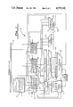
- FIG. 1 shows a block diagram of a floating point arithmetic circuit used with the present invention
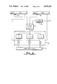
- FIG. 2 shows a block diagram of the divisor multiple selection circuits
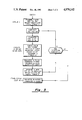
- FIG. 3 shows a flow chart of the method for sequencing the apparatus of FIG. 1 and FIG. 2.
- FIG. 1 there is shown a block diagram of the floating point arithmetic circuit which is used in conjunction with the present invention.
- the execution of floating point arithmetic utilizes this circuit because of the specific algorithms which must be performed to determine the proper results.
- This circuit presumes that the floating point numbers have been prearranged according to a particular format, where the most significant bit represents the sign of the floating point number, and wherein a group of the next-most significant bits represent the exponent of the floating point number, and wherein the remaining bits represent the fraction value of the number; i.e., the fraction value presuming that decimal point is placed at the left-most end of the fraction value.
- the hardware registers and logic associated with FIG. 1 include four additional bits; the I bit occupies the most significant position in the fraction field, and the G, R and S bits respectively occupy the least significant bit positions in the fraction field.
- Floating point operands cannot be added to or subtracted from each other unless their exponents are equal. This requires that their exponents be compared, and the operand fraction with the smaller exponent be shifted the amount of the exponent difference. The fractions can then be added or subtracted with the larger exponent as the result exponent. Multiplication of floating point operands requires that the exponents be added and the fractions multiplied. Division of floating point operands requires that the divisor exponent be subtracted from the dividend exponent and the dividend fraction be divided by the divisor fraction.
- the floating point arithmetic circuit of FIG. 1 can support both single and double precision arithmetic operations. It is designed to support a floating point add or subtract operation, a multiply operation that retires 4 bits of multiplier per iteration, and a divide operation that generates two quotient bits per iteration.
- the floating point arithmetic circuit 10 of FIG. 1 utilizes a storage data buss 12 for receiving and transmitting data from other sources, such as a data processing system or the like. Information received over data storage buss 12 may be transmitted into a plurality of floating point registers 14. In the preferred embodiment there are eight floating point registers 14, each adapted to hold the floating point operands and the results of floating point operations. Floating point registers 14 may transmit information to an FA register 16, an FB register 18, or an FC register 22. FA register 16 may also transmit information back to floating point registers 14.
- the FA register 16 is a destination register for data from the floating point registers 14, and is the source register for data being transmitted to the floating point registers 14.
- the FA register 16 is also the source register for data which may be transferred to a memory via storage data buss 12, and it is a destination register for data transmitted from the carry-propagate adder 30, the exponent adder 20, and from the normalize-round circuit 34.
- the FA register 16 has outputs to the multiple selector 24, the prealigner circuit 26, the normalize-round circuit 34, and the exponent adder 20.
- the FA register 16 contains the second operand for add, subtract, compare, multiply and divide operations.
- FA register 16 has a section 16a for holding the exponent of the floating point number, and a section 16b for holding the fraction portion of the floating point number.
- the FA register 16 In order to selectively control which of the plurality of inputs to the FA register 16 are to be gated into the register, the FA register 16 has an input multiplexer circuit 15 associated therewith. Multiplexer circuit 15 provides for the selective gating of the various inputs into register 16, under control of an activation signal A. Other registers in the floating point arithmetic circuit 10 have similar multiplexer input controls.
- a control logic circuit 11 generates all of the activation signals required for data interchange and processing operations within floating point arithmetic circuit 10.
- Control logic circuit 11 has a plurality of control signal outputs, designated A, each of which serve as control inputs to various circuits and registers. It is well within the skill of the art to understand the need and design for a control logic circuit 11, as well as the activation signals A which are required for the operation of floating point arithmetic circuit 10; accordingly, a detailed presentation of these circuits and signals is not required herein.
- Control logic circuit 11 also receives the most significant three bits from the FA register section 16b, and from the FB register 18b; it also receives the most significant three bits from the carry-propagate adder 30 via 3-bit decode circuit 36.
- Control logic 11 has decoding circuitry therein for decoding the respective 3-bit values, and for activating a particular activation signal A' which is transmitted to the multiple selector logic 24 for the purpose of selecting appropriate latches. Control logic 11 also has decoding logic for detecting whether the FB register section 18b value is true or complement, for detecting whether the carry-propagate adder 30 output is true or complement, and for detecting the particular latch signal A' which has been activated during any divide iteration. Control logic 11 utilizes these signals to generate a 2 or 3-bit quotient value Q, which it transfers to the lower two positions of the input multiplexer section 21, associated with FC register 22.
- the FB register 18 is a destination register for data received from the storage data buss 12, the floating point registers 14, and is also a destination register for data from the carry-propagate adder 30. It has outputs to the multiple selector 24, the prealigner circuit 26, and the exponent adder 20.
- the FB register is used to contain the first operand for the add, subtract, compare and divide operations; it also contains the intermediate result of the add, subtract, multiply, and divide operations.
- the FB register 18 has a section 18a for containing the exponent value of the floating point number, and a section 18b for containing the fraction portion of the floating point number, and has an input multiplexer circuit 17 for gating data into the register under control of activation signals from control logic circuit 11. For divide it contains the dividend and subsequent partial dividends.
- the FC register 22 is a destination register for data from memory via storage data buss 12, and a destination register for data from the normalize-round circuit 34. It is also the destination register from the floating point registers 14.
- the FC register 22 has outputs to the multiple selector 24, the prealigner circuit 26, and the normalize-round circuit 34.
- the FC register 22 is used to contain the first operand of the multiply operation, and it is the destination register for the quotient of a divide operation.
- An input multiplexer circuit 21 controls the gating of data into FC register 22, under control of activation signals from control logic circuit 11.
- the exponent adder 20 is a 13-bit adder circuit that is used for exponent arithmetic. It handles the exponent calculations for either single or double precision exponents.
- the exponent adder is a source for data transmitted to FA register section 16a, and FB register section 18a.
- the exponent adder 20 has an input multiplexer circuit 19.
- the prealigner circuit 26 is used to pre-shift the fraction with the smaller exponent for the add and subtract operation, which is necessary to make the floating point operand exponents equal prior to an add or subtract operation.
- the prealigner circuit 26 has the capability to shift a floating point fraction right from 0 to 55 bit positions, depending upon whether single or double precision arithmetic is being performed.
- the prealigner circuit 26 has an output to the carry-propagate adder 30, and to the FC register 22.
- the multiple selector 24 is a logic circuit which gates multiples of the multiplicand for the multiply operation, and multiples of the divisor for the divide operation. For the divide operation, the multiples are by the control logic 11 from a decoding of the high-order bits of the dividend, or partial dividend, and of the divisor. The complement of the operand may be generated by the multiple selector when necessary.
- the multiple selector 24 receives data from the FA register 16, the FB register 18, and the FC register 22. The multiple selector 24 has outputs to the carry-save adder 28.
- the carry-save adder 28 will permit three operands to be added together at the same time. This permits the use of a divide algorithm which generates two quotient bits per iteration.
- the carry-save adder 28 receives data from the multiple selector 24, and transmits data to the carry-propagate adder 30.
- the carry-save adder 28 may operate according to the principal of 2's complement subtraction, but in any event the results it produces for division are effectively to subtract the divisor (or a multiple of the divisor) from the dividend (or partial dividend) to form a quotient (or partial quotient) over a series of iterations, in conjunction with the carry-propagate adder 30.
- the carry-propagate adder 30 is a 57-bit adder, and has an input from the carry-save adder 28 for generating the partial product of a multiply operation or the partial dividend of a divide operation.
- the carry-propagate adder circuit 30 may also receive inputs from the prealigner circuit 26, the FA register 16, and the FB register 18.
- the carry-propagate adder has an output connection to the FA register 16 and the FB register 18.
- An input multiplexer circuit 29 controls the gating of data into carry-propagate adder 30, under control of activation signals A from control logic circuit 11.
- the most significant bits output from the carry-propagate adder 30 are monitored by a 3-bit decode circuit 36, for use in connection with the divide operation to be hereinafter described.
- the normalize-round circuit 34 includes a normalize circuit 34a which is used to normalize the results of a floating point operation. For example, the result of a multiply operation may require a right-shift of one bit in order to normalize the fraction, and the result of an add or subtract operation may require a left-shift of up to 54 bit positions.
- the normalize-round circuit 34 also includes a round circuit 34b, which contains an incrementor circuit, for use in certain rounding operations, where the result may have to be incremented by a value of 1 in the low-order bit position.
- both the divisor and the dividend must be normalized.
- the divisor is initially placed into the FA register 16, and the dividend is initially placed in the FB register 18.
- the divisor is normalized by gating the fractional quantity found in FA register 16b into the prealigner circuit 26, shifting the fractional quantity left by the number of leading zeros in the fraction field, and restoring the shifted value back into the FA register 16b.
- the number of shifts recorded is subtracted from the exponent value initially contained in FA register 16a, by a subtraction operation performed in the exponent adder circuit 20. After this subtraction is performed the subtracted value is gated back into the FA register exponent portion 16a.
- the dividend is normalized by gating the fractional quantity found in FB register 18b to the normalizer 34a, shifting it left by the number of leading zeros found in the fraction, and restoring the shifted value back to the FB register 18b.
- the exponent value in FB register 18a is subtracted by the number of shifts recorded from the fraction shift operation, through the exponent adder circuit 20, and the subtracted value of the exponent is restored into FB register 18a.
- An initialization cycle is required for the divide iterations. This is accomplished by initializing a counter to count the iterations; 13 for single precision, and 28 for double precision.
- the three most significant bits of the fractions in the FA register 16b and the FB registers 18b are monitored by control logic 11 to determine the divisor multiple which is to be used for the first iteration. The determination of this multiple Will be described hereinafter, with reference to FIGS. 2 and 3.
- the exponents in the FA register 16a and the FB register 18a are gated to the exponent adder, and the FA exponent is subtracted from the FB exponent, with the result being placed into the FA register 16a.
- the divide sequence requires a non-restoring uniform shift of two bits during each iteration. It requires the 0, 1/2, 3/4, 1, and 3/2 multiples of the divisor to be selectable by the multiple selector 24, to produce a partial dividend that can be shifted left by two bits for each iteration, and which will produce two quotient bits for each iteration. The quotient ultimately will appear in the FC register 22, and the partial dividends will be developed in register section 18b during the operation.
- FIG. 2 shows a portion of the floating point arithmetic circuit 10 of FIG. 1, which is associated with the selection of the divisor multiple to be used during each iteration of the divide operation.
- control logic 11 monitors the most significant three bits of register 16b, designated 16b' in FIG. 2, and also monitors the most significant three bits of register 18b, designated 18b' in FIG. 2.
- Control logic 11 utilizes these quantities in its internal decision logic to determine the initial divisor multiple to be used in the divide operation. This determination results in the generation of a particular activation signal A', which is coupled to one or more latches in multiple selector 24. The respective latches permit selective gating of the fractional divisor held in register 16b into carry-save adder 28.
- one A' signal will activate the latch designated 1:1, which permits the fractional contents of register 16b to be directly transferred to an input of carry-save adder 28;
- another activation signal A' activates the latch designated 1:1/2, which permits the fractional contents of register 16b to be gated to an input of carry-save adder 28, which with each bit shifted one position rightward from its respective position in register 16b;
- a third activation signal A' activates a latch 1:1/4, which permits the gating of the fractional contents of register 16b into an input of carry-save adder 28, shifted two bit positions to the right from the respective position of the fraction in register 16b.
- control logic 11 can generate an activation signal A' which gates either the divisor, or 1/2 divisor, or 1/4 divisor into carry-save adder 28 inputs. Since carry-save adder 28 has three inputs, and is capable of adding the values represented at these three inputs, it is possible to combine activation of two latches to provide a combinatorial multiple, for example, if the latch designated 1:1/2 and the latch designated 1:1/4 are both activated, 1/2 divisor will appear at one carry-save adder 28 input and 1/4 divisor will appear at a second carry-save adder input, the sum of which will equal 3/4 divisor.
- the divisor and 1/2 divisor are simultaneously gated to inputs of the carry-save adder 28, the sum of which will produce 3/2's divisor.
- the zero divisor can be produced by merely inhibiting all gating from register 16b into carry-save adder 28, thereby producing a zero input to carry-save adder 28. Therefore, it is readily possible for control logic 11 to produce the zero, 1/2, 3/4, 1, and 3/2 multiples of the divisor during any iteration of the divide cycle.
- control logic 11 selects the divisor multiple for subsequent iterations through examination of the most significant three bits output from the carry-propagate adder 30, via a 3-bit decode circuit 36.
- Control logic 11 is also coupled to register 18b and carry-propagate adder 30 to sense the most significant fractional carry bit to determine whether the current value is a true or complement number, particularly comparing the value of the partial dividend both before and after each iteration. This comparison, together with an examination of the divisor multiple used during the iteration, enables the circuit to predict whether the subtraction operation which occurs during the iteration has changed the sign of the partial dividend. If the sign has changed, the divisor multiple selected is too large, and the resulting quotient bits should be reduced or increased by a predetermined value, dependent upon the multiple used for the iteration. Control logic 11 contains an internal decision circuit which enables this comparison to be made, and which results in the selection of the appropriate quotient, dependent upon these variables.
- the quotient may be a 2-bit quotient Q, or in certain instances a 3-bit quotient Q. In the one case where a divisor multiple of 3/4 is used during the iteration, a 3-bit quotient is produced; in all other instances a 2-bit quotient value is produced. In the case of a 3-bit quotient value, and in the case of a 2-bit quotient value, the value itself is transferred to input multiplexer section 21 at the lowest two (or three) bit positions. If a 3-bit quotient value is selected, the most significant quotient bit produced as a result of the next iteration is ignored, and the next iteration results in the transfer of a 1-bit quotient value to the input multiplexer 21.
- TABLE 1 shows a table for selecting the divisor multiple as a function of the dividend, or partial dividend.
- the high-order three bits of the divisor and the high-order three bits of the dividend are decoded according to the tabulation of TABLE 1 to select the multiple of the divisor for the next iteration. For example, if the high-order three bits of the true dividend are 011, and the high-order two bits of the divisor are 110, the multiple of the divisor for the next iteration which is selected will be the 1/2 times multiple of the divisor.
- the decoding conventions shown in TABLE 1 insures that the partial dividend can be shifted two bit positions and therefore, at least two quotient bit positions bits can be generated.
- TABLE 2 shows a table for selecting at least a pair of quotient bits as a function of the partial dividend value and the divisor multiplier selected, according to non-restoring division techniques.
- the quotient bits which are selected depend upon three conditions:
- the quotient bits selected will be 01. In the case when the 3/4 times multiple is used during the iteration, three quotient bits are generated. These three quotient bits are all valid, and the third bit must be used in place of the high-order bit that is generated on the next iteration.
- FIG. 3 shows a flow chart of the divide iterations according to the teachings of the present invention.
- the left side of FIG. 3 illustrates the machine cycles which are required for divide iterations, wherein cycle 1 is defined as an initial cycle for setting up the first iteration, and cycles 2-14 are the iteration cycles for single precision numbers (cycles 2-29 for double precision numbers), and the final cycle is devoted to postnormalized and round operations.
- the postnormalize and round operations may be accomplished according to the teachings of copending U.S. Pat. applications Ser. No. 339,348, now U.S. Pat. No. 4,926,370, issued May 15, 1990, and Ser. No. 339,268, filed of even date herewith, or may be accomplished according to usual techniques which are well known in the art.
- control logic 11 In cycle 1 of the divide operation, the three most significant bits of the fractional quantity contained in register 16b and register 18b are examined and decoded by control logic 11. Control logic 11 then generates an activation signal A' for selecting a particular multiple latch as has been hereinbefore described, and which results in the selection of the multiple illustrated in Table 1.
- the binary value contained in register 16b is gated into carry-save adder 28 via the latching network hereinbefore described, and is subtracted from the binary value contained in register 18b.
- the subtracted value may be any of the five multiples of the divisor which have been described.
- the results of this subtraction are transferred from the carry-propagate adder 30 to input multiplexer section 17; the most significant three bits of the result from carry-propagate adder 30 is received by the 3-bit decode circuit 36.
- Control logic 11 then senses the three most significant bits in register 16b, and the 3-bit value found in decode circuit 36, and determines whether the respective values are true or complement values; control logic 11 also checks the multiple latch which was selected for the last subtraction. Control logic 11 then generates a 2-bit quotient Q (3-bits if multiplier was 3/4), wherein Q is generated from an internal decision circuit which is illustrated in Table 2.
- Control logic 11 then transfers the Q value to input multiplexer section 21, at the least significant bit positions, and then transfers the input multiplexer section 21 contents into register 22, two bit positions to the left of the least significant bit. Control logic 11 also transfers the input multiplexer 17 into register 18b to form the new partial dividend.
- Control logic 11 then examines the three most significant bits in register 16b, and also examines the contents of 3-bit decode circuit 36, to make a determination through internal decision logic as to the selection of the next multiple. This multiple is selected according to the internal decision logic which is illustrated in Table 1. A new subtraction is made, and this process continues until all of the iterations for the particular divide operation have been completed.
- control logic circuit 11 transfers the contents of register 18 into the normalize and round circuits 34a and 34b for postnormalize and round operations, according to the teachings of the art.
- Postnormalize and round occurs during a final cycle of the divide operation, and at the completion of the divide operation the quotient is found in register 22, the remainder is found in register 18, and the original divisor is still found in register 16.
Landscapes
- Physics & Mathematics (AREA)
- General Physics & Mathematics (AREA)
- Engineering & Computer Science (AREA)
- Computational Mathematics (AREA)
- Mathematical Analysis (AREA)
- Mathematical Optimization (AREA)
- Pure & Applied Mathematics (AREA)
- Theoretical Computer Science (AREA)
- Computing Systems (AREA)
- General Engineering & Computer Science (AREA)
- Complex Calculations (AREA)
- Error Detection And Correction (AREA)
Priority Applications (3)
| Application Number | Priority Date | Filing Date | Title |
|---|---|---|---|
| US07/339,261 US4979142A (en) | 1989-04-17 | 1989-04-17 | Two-bit floating point divide circuit with single carry-save adder |
| EP19900480033 EP0394162A3 (de) | 1989-04-17 | 1990-03-07 | Zweibit-Gleitkomma-Divisionsschaltung mit nur einem Übertragsicherstellungsaddierer |
| JP2099454A JPH02294821A (ja) | 1989-04-17 | 1990-04-17 | 浮動小数点数演算処理装置 |
Applications Claiming Priority (1)
| Application Number | Priority Date | Filing Date | Title |
|---|---|---|---|
| US07/339,261 US4979142A (en) | 1989-04-17 | 1989-04-17 | Two-bit floating point divide circuit with single carry-save adder |
Publications (1)
| Publication Number | Publication Date |
|---|---|
| US4979142A true US4979142A (en) | 1990-12-18 |
Family
ID=23328209
Family Applications (1)
| Application Number | Title | Priority Date | Filing Date |
|---|---|---|---|
| US07/339,261 Expired - Fee Related US4979142A (en) | 1989-04-17 | 1989-04-17 | Two-bit floating point divide circuit with single carry-save adder |
Country Status (3)
| Country | Link |
|---|---|
| US (1) | US4979142A (de) |
| EP (1) | EP0394162A3 (de) |
| JP (1) | JPH02294821A (de) |
Cited By (9)
| Publication number | Priority date | Publication date | Assignee | Title |
|---|---|---|---|---|
| US5105378A (en) * | 1990-06-25 | 1992-04-14 | Kabushiki Kaisha Toshiba | High-radix divider |
| US5128891A (en) * | 1990-04-02 | 1992-07-07 | Advanced Micro Devices, Inc. | High speed divider with square root capability |
| US5237525A (en) * | 1992-06-01 | 1993-08-17 | Motorola, Inc. | In a data processor an SRT divider having a negative divisor sticky detection circuit |
| US5258944A (en) * | 1992-09-01 | 1993-11-02 | Cray Research, Inc. | High performance mantissa divider |
| US5272660A (en) * | 1992-06-01 | 1993-12-21 | Motorola, Inc. | Method and apparatus for performing integer and floating point division using a single SRT divider in a data processor |
| US5301139A (en) * | 1992-08-31 | 1994-04-05 | Intel Corporation | Shifter circuit for multiple precision division |
| US5357455A (en) * | 1992-10-09 | 1994-10-18 | Intel Corporation | Floating point remainder generator for a math processor |
| US5386376A (en) * | 1992-08-31 | 1995-01-31 | Intel Corporation | Method and apparatus for overriding quotient prediction in floating point divider information processing systems |
| US5548544A (en) * | 1994-10-14 | 1996-08-20 | Ibm Corporation | Method and apparatus for rounding the result of an arithmetic operation |
Families Citing this family (1)
| Publication number | Priority date | Publication date | Assignee | Title |
|---|---|---|---|---|
| EP1785862A3 (de) * | 2000-02-29 | 2007-08-15 | Fujitsu Limited | Verfahren und Vorrichtung zur Pipeline-Verarbeitung |
Citations (4)
| Publication number | Priority date | Publication date | Assignee | Title |
|---|---|---|---|---|
| US3591787A (en) * | 1968-01-29 | 1971-07-06 | Ibm | Division system and method |
| US3684879A (en) * | 1970-09-09 | 1972-08-15 | Sperry Rand Corp | Division utilizing multiples of the divisor stored in an addressable memory |
| US3733477A (en) * | 1972-02-04 | 1973-05-15 | Control Data Corp | Iterative binary divider utilizing multiples of the divisor |
| US3852581A (en) * | 1972-12-14 | 1974-12-03 | Burroughs Corp | Two bit binary divider |
Family Cites Families (1)
| Publication number | Priority date | Publication date | Assignee | Title |
|---|---|---|---|---|
| JPS5135245A (de) * | 1974-09-20 | 1976-03-25 | Hitachi Ltd |
-
1989
- 1989-04-17 US US07/339,261 patent/US4979142A/en not_active Expired - Fee Related
-
1990
- 1990-03-07 EP EP19900480033 patent/EP0394162A3/de not_active Ceased
- 1990-04-17 JP JP2099454A patent/JPH02294821A/ja active Pending
Patent Citations (4)
| Publication number | Priority date | Publication date | Assignee | Title |
|---|---|---|---|---|
| US3591787A (en) * | 1968-01-29 | 1971-07-06 | Ibm | Division system and method |
| US3684879A (en) * | 1970-09-09 | 1972-08-15 | Sperry Rand Corp | Division utilizing multiples of the divisor stored in an addressable memory |
| US3733477A (en) * | 1972-02-04 | 1973-05-15 | Control Data Corp | Iterative binary divider utilizing multiples of the divisor |
| US3852581A (en) * | 1972-12-14 | 1974-12-03 | Burroughs Corp | Two bit binary divider |
Non-Patent Citations (2)
| Title |
|---|
| Jackson et al., "Binary Multiplication & Division Utilizing a Three-Input Adder" IBM Tech. Disclosure Bulletin, vol. 15, No. 7, Dec. 1972, pp. 2263-2268. |
| Jackson et al., Binary Multiplication & Division Utilizing a Three Input Adder IBM Tech. Disclosure Bulletin, vol. 15, No. 7, Dec. 1972, pp. 2263 2268. * |
Cited By (9)
| Publication number | Priority date | Publication date | Assignee | Title |
|---|---|---|---|---|
| US5128891A (en) * | 1990-04-02 | 1992-07-07 | Advanced Micro Devices, Inc. | High speed divider with square root capability |
| US5105378A (en) * | 1990-06-25 | 1992-04-14 | Kabushiki Kaisha Toshiba | High-radix divider |
| US5237525A (en) * | 1992-06-01 | 1993-08-17 | Motorola, Inc. | In a data processor an SRT divider having a negative divisor sticky detection circuit |
| US5272660A (en) * | 1992-06-01 | 1993-12-21 | Motorola, Inc. | Method and apparatus for performing integer and floating point division using a single SRT divider in a data processor |
| US5301139A (en) * | 1992-08-31 | 1994-04-05 | Intel Corporation | Shifter circuit for multiple precision division |
| US5386376A (en) * | 1992-08-31 | 1995-01-31 | Intel Corporation | Method and apparatus for overriding quotient prediction in floating point divider information processing systems |
| US5258944A (en) * | 1992-09-01 | 1993-11-02 | Cray Research, Inc. | High performance mantissa divider |
| US5357455A (en) * | 1992-10-09 | 1994-10-18 | Intel Corporation | Floating point remainder generator for a math processor |
| US5548544A (en) * | 1994-10-14 | 1996-08-20 | Ibm Corporation | Method and apparatus for rounding the result of an arithmetic operation |
Also Published As
| Publication number | Publication date |
|---|---|
| JPH02294821A (ja) | 1990-12-05 |
| EP0394162A3 (de) | 1992-07-01 |
| EP0394162A2 (de) | 1990-10-24 |
Similar Documents
| Publication | Publication Date | Title |
|---|---|---|
| US4926370A (en) | Method and apparatus for processing postnormalization and rounding in parallel | |
| US4941120A (en) | Floating point normalization and rounding prediction circuit | |
| EP0421092B1 (de) | Verfahren und Gerät zur Ausführung mathematischer Funktionen mit Hilfe polynomialer Annäherung und eines Multiplizierers rechteckigen Seitenverhältnisses | |
| US5995991A (en) | Floating point architecture with tagged operands | |
| EP0040279B1 (de) | Binärer Dividierer | |
| US10078512B2 (en) | Processing denormal numbers in FMA hardware | |
| KR20080055985A (ko) | 선택가능 준정밀도를 가진 부동―소수점 프로세서 | |
| JPH02294730A (ja) | 浮動小数点数演算処理装置 | |
| US5132925A (en) | Radix-16 divider using overlapped quotient bit selection and concurrent quotient rounding and correction | |
| JPH01112332A (ja) | 乗算及び算術論理演算機能を組合わせて使用する浮動小数点ユニット | |
| US4979142A (en) | Two-bit floating point divide circuit with single carry-save adder | |
| US4996660A (en) | Selection of divisor multipliers in a floating point divide circuit | |
| JPH05216620A (ja) | 浮動小数点を正規化する方法及び回路 | |
| US5790444A (en) | Fast alignment unit for multiply-add floating point unit | |
| USH1222H (en) | Apparatus for determining sticky bit value in arithmetic operations | |
| JPH05250146A (ja) | 整数累乗処理を行なうための回路及び方法 | |
| US5734599A (en) | Performing a population count using multiplication | |
| EP0505175B1 (de) | Vorprozessor für Dividierer unter Verwendung eines Divisionssystems mit hoher Grundzahl | |
| US5867413A (en) | Fast method of floating-point multiplication and accumulation | |
| US5117384A (en) | Method and apparatus for exponent adder | |
| US6598065B1 (en) | Method for achieving correctly rounded quotients in algorithms based on fused multiply-accumulate without requiring the intermediate calculation of a correctly rounded reciprocal | |
| US4979141A (en) | Technique for providing a sign/magnitude subtraction operation in a floating point computation unit | |
| US5150319A (en) | Circuitry for rounding in a floating point multiplier | |
| GB2265739A (en) | Non-restore division with dividend-width ALU | |
| EP0137525B1 (de) | Arithmetische Einheit mit Bit-Ausbreitungsschaltung in einem Datenverarbeitungssystem |
Legal Events
| Date | Code | Title | Description |
|---|---|---|---|
| AS | Assignment |
Owner name: INTERNATIONAL BUSINESS MACHINES CORPORATION, A COR Free format text: ASSIGNMENT OF ASSIGNORS INTEREST.;ASSIGNORS:ALLEN, RICHARD G.;FREERKSEN, DONALD L.;REEL/FRAME:005081/0683 Effective date: 19890414 |
|
| FPAY | Fee payment |
Year of fee payment: 4 |
|
| REMI | Maintenance fee reminder mailed | ||
| LAPS | Lapse for failure to pay maintenance fees | ||
| FP | Lapsed due to failure to pay maintenance fee |
Effective date: 19981218 |
|
| STCH | Information on status: patent discontinuation |
Free format text: PATENT EXPIRED DUE TO NONPAYMENT OF MAINTENANCE FEES UNDER 37 CFR 1.362 |