US4937638A - Edge emitting light emissive diode - Google Patents
Edge emitting light emissive diode Download PDFInfo
- Publication number
- US4937638A US4937638A US07/239,403 US23940388A US4937638A US 4937638 A US4937638 A US 4937638A US 23940388 A US23940388 A US 23940388A US 4937638 A US4937638 A US 4937638A
- Authority
- US
- United States
- Prior art keywords
- active region
- chip
- facet
- axis
- range
- Prior art date
- Legal status (The legal status is an assumption and is not a legal conclusion. Google has not performed a legal analysis and makes no representation as to the accuracy of the status listed.)
- Expired - Lifetime
Links
Images


Classifications
-
- H—ELECTRICITY
- H10—SEMICONDUCTOR DEVICES; ELECTRIC SOLID-STATE DEVICES NOT OTHERWISE PROVIDED FOR
- H10H—INORGANIC LIGHT-EMITTING SEMICONDUCTOR DEVICES HAVING POTENTIAL BARRIERS
- H10H20/00—Individual inorganic light-emitting semiconductor devices having potential barriers, e.g. light-emitting diodes [LED]
- H10H20/80—Constructional details
- H10H20/81—Bodies
- H10H20/819—Bodies characterised by their shape, e.g. curved or truncated substrates
-
- H—ELECTRICITY
- H01—ELECTRIC ELEMENTS
- H01S—DEVICES USING THE PROCESS OF LIGHT AMPLIFICATION BY STIMULATED EMISSION OF RADIATION [LASER] TO AMPLIFY OR GENERATE LIGHT; DEVICES USING STIMULATED EMISSION OF ELECTROMAGNETIC RADIATION IN WAVE RANGES OTHER THAN OPTICAL
- H01S5/00—Semiconductor lasers
- H01S5/06—Arrangements for controlling the laser output parameters, e.g. by operating on the active medium
- H01S5/0601—Arrangements for controlling the laser output parameters, e.g. by operating on the active medium comprising an absorbing region
-
- H—ELECTRICITY
- H01—ELECTRIC ELEMENTS
- H01S—DEVICES USING THE PROCESS OF LIGHT AMPLIFICATION BY STIMULATED EMISSION OF RADIATION [LASER] TO AMPLIFY OR GENERATE LIGHT; DEVICES USING STIMULATED EMISSION OF ELECTROMAGNETIC RADIATION IN WAVE RANGES OTHER THAN OPTICAL
- H01S5/00—Semiconductor lasers
- H01S5/10—Construction or shape of the optical resonator, e.g. extended or external cavity, coupled cavities, bent-guide, varying width, thickness or composition of the active region
- H01S5/1053—Comprising an active region having a varying composition or cross-section in a specific direction
- H01S5/1064—Comprising an active region having a varying composition or cross-section in a specific direction varying width along the optical axis
-
- H—ELECTRICITY
- H01—ELECTRIC ELEMENTS
- H01S—DEVICES USING THE PROCESS OF LIGHT AMPLIFICATION BY STIMULATED EMISSION OF RADIATION [LASER] TO AMPLIFY OR GENERATE LIGHT; DEVICES USING STIMULATED EMISSION OF ELECTROMAGNETIC RADIATION IN WAVE RANGES OTHER THAN OPTICAL
- H01S5/00—Semiconductor lasers
- H01S5/20—Structure or shape of the semiconductor body to guide the optical wave ; Confining structures perpendicular to the optical axis, e.g. index or gain guiding, stripe geometry, broad area lasers, gain tailoring, transverse or lateral reflectors, special cladding structures, MQW barrier reflection layers
- H01S5/22—Structure or shape of the semiconductor body to guide the optical wave ; Confining structures perpendicular to the optical axis, e.g. index or gain guiding, stripe geometry, broad area lasers, gain tailoring, transverse or lateral reflectors, special cladding structures, MQW barrier reflection layers having a ridge or stripe structure
-
- H—ELECTRICITY
- H10—SEMICONDUCTOR DEVICES; ELECTRIC SOLID-STATE DEVICES NOT OTHERWISE PROVIDED FOR
- H10H—INORGANIC LIGHT-EMITTING SEMICONDUCTOR DEVICES HAVING POTENTIAL BARRIERS
- H10H20/00—Individual inorganic light-emitting semiconductor devices having potential barriers, e.g. light-emitting diodes [LED]
- H10H20/80—Constructional details
- H10H20/81—Bodies
- H10H20/816—Bodies having carrier transport control structures, e.g. highly-doped semiconductor layers or current-blocking structures
- H10H20/8162—Current-blocking structures
-
- H—ELECTRICITY
- H10—SEMICONDUCTOR DEVICES; ELECTRIC SOLID-STATE DEVICES NOT OTHERWISE PROVIDED FOR
- H10H—INORGANIC LIGHT-EMITTING SEMICONDUCTOR DEVICES HAVING POTENTIAL BARRIERS
- H10H20/00—Individual inorganic light-emitting semiconductor devices having potential barriers, e.g. light-emitting diodes [LED]
- H10H20/80—Constructional details
- H10H20/83—Electrodes
- H10H20/831—Electrodes characterised by their shape
-
- H—ELECTRICITY
- H10—SEMICONDUCTOR DEVICES; ELECTRIC SOLID-STATE DEVICES NOT OTHERWISE PROVIDED FOR
- H10H—INORGANIC LIGHT-EMITTING SEMICONDUCTOR DEVICES HAVING POTENTIAL BARRIERS
- H10H20/00—Individual inorganic light-emitting semiconductor devices having potential barriers, e.g. light-emitting diodes [LED]
- H10H20/80—Constructional details
- H10H20/83—Electrodes
- H10H20/832—Electrodes characterised by their material
Definitions
- This invention relates to light emissive diodes (LED's), and in particular to those of the edge-emissive variety (ELED's).
- Lasers and superluminescent diodes typically have greater brightnesses than non-superluminescent diodes but for number of applications the benefits of this increased brightness are outweighed by the disadvantage of the much greater temperature sensitivity of lasers and superluminescent diodes.
- Characteristically a non-superluminescent device exhibits saturation effects in which the rate of increase of light output with increasing drive current begins to fall off at high current drive, whereas in the case of a superluminescent device the characteristic is one of ever-increasing rate of increase of light output with increasing current drive up at least until the lasing threshold is reached.
- This invention is specifically directed to ELED's which over a normal operating current range of 0 to 100 mA are substantially non-superluminescent at least down to a temperature of 10° and preferably over the temperature range from 0° to 70° C.
- Devices which show no signs of superluminescence over this temperature range may begin to show signs of superluminescence at much lower temperatures as a result primarily of the reduction in non-radiactive recombination liable to occur at temperatures significantly beneath 0° C., but for many applications such temperatures lie far enough beneath typical service temperatures, and hence such devices will exhibit substantially no superluminescence in the course of normal use.
- the lasing threshold current still lies outside the normal operating current range of 0 to 100 mA.
- a stripe contact double heterosctucture ELED provides an acceptable source for launching short coherence length (non-laser) light into conventional multimode fibre.
- the stripe contact may be arranged to terminate short of the rear end of diode. By terminating the stripe contact well short of one end of the semiconductor chip there is left an unpumped region of the chip beyond the end of the stripe. This unpumped region will remain optically obsorbing and hence minimise optical feedback that would otherwise tend to promote laser action. Examples of such ELED's with full length stripe contacts and with truncated stripe contacts are described for instance in United Kingdom Patent Specification No. 1,600,965.
- the semiconductor lasers are planar, and their composition is chosen to provide a refractive index profile that affords a real waveguiding effect in the direction normal to those layers.
- planar layers produce no lateral waveguiding effect, that is no waveguiding effect in the plane of the layers.
- the injected carriers under the stripe have the effect of reducing the effective refractive of the material and hence when the device is driven the resulting index profile in the transverse direction (lying in the plane of the layers at right angles to the stripe axis) tends to be anti-waveguiding.
- the present invention is directed to non-superluminescent ELED's suitable for coupling to single mode fibre, and arose out of attempts to launch more optical power into single mode optical fibre than can be conveniently and easily be launched from a truncated stripe contact non-superluminescent ELED, but which retains the desirable relative stability of output power with temperature variation which is observed in stripe contact non-superluminescent ELED's.
- an electroded edge emissive light emissive diode chip which is structured to confine current injection across the p-n junction of the diode substantially exclusively to an active region that extends along an axis from substantially one end facet of the chip, the output facet, to a point intermediate said output facet and the opposite end facet, which chip has a refractive index structure providing, for the active region, real optical waveguiding in all directions at right angles to said axis, and, for the region of the chip extending along the axis beyond the active region between said intermediate point and said opposite facet, no real optical waveguiding for at least one direction at right angles to said axis, wherein the active region is short enough substantially to prevent superluminescence at least down to a temperature of 10° C. over an operating current range of 0 to 100 mA, and wherein in the active region the refractive index profile is such as to provide substantially single mode waveguiding for matching with that of a single mode fibre.
- a preferred way of providing this lateral waveguiding effect in ELED's constructed in accordance with the teachings of the present invention is by adopting a ridge structure in which the effective refractive index of a planar active layer bounded on both faces by lower refractive index material is locally raised by the presence of an overlying ridge of material protruding into material of a lower refractive index.
- FIG. 1 is a schematic perspective view of the device prior to the etching of the channels which define the ridge structure.
- FIG. 2 is a schematic perspective view of the completed device.
- FIG. 3 depicts the device mounted upon a heat sink.
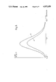
- FIGS. 4 and 5 are plots of near field intensity profiles
- FIGS. 6 and 7 are plots showing the relationship between drive current and light output at different temperatures of operation.
- FIG. 8 is a plot of the spectral characteristic at two different levels of current drive.
- a succession of layers 2, 3, 4, 5 and 6 is epitaxially grown upon an n + -type indium phosphide (InP) substrate 1.
- InP indium phosphide
- the first epitaxial layer to be grown, layer 2 is an n-type InP buffer layer. This layer is typically between 2 and 5 ⁇ min thickness. Its growth is succeeded by the growth of layer 3 which is the active layer of the device.
- the active layer is thinner, typically being in the range from 0.08 ⁇ m to 0.50 ⁇ m in thickness.
- the active layer is made of p-type or n-type InGaAsP, and its composition is chosen having regard to the wavelength of emission required from the device.
- the composition of the active layer 3 is In.sub..71 Ga.sub..29 As.sub..62 P.sub..38 and its thickness is 0.15 um.
- Layer 4 is a p-type anti-meltback/guide layer, also of quaternary InGaAsP, but of a composition corresponding to a shorter emission wavelength than that of the active layer, typically a composition corresponding to an emission wavelength of 1.18 ⁇ m or 1.06 ⁇ m.
- the thickness of this layer 4 lies typically in the range 0.1 to 0.3 ⁇ m.
- a thickness of 0.25 ⁇ m is preferred for use with the 0.15 ⁇ m thickness active layer.
- the remaining epitaxial layers of the structure, layers 5 and 6, are respectively a p-type cladding layer of InP which is typically about 1.5 ⁇ m thick, and a p-type contact layer of InGaAsP which is typically about 0.2 ⁇ m thick and may conveniently have the same composition as that of layer 4.
- wet chemical etching is employed to etch two channels through the contact and cladding layers 6 and 5 so as to define an intervening ridge 7 that is typically between 3 and 5 ⁇ m in width.
- the length of the channels is shorter than the equivalent dimension of the substrate so that the ridge 7 extends outwardly from a planar region 8.
- These channels are etched through an oxide mask (not shown) after photolithography.
- a KKI-type etch is used to remove the quaternary material of layer 6.
- An H 3 PO 4 : HCl etch is used for removal of the InP of layer 5 since, with this etch, etching is substantially halted upon exposure of the underlying quaternary material of the anti-meltback/guide layer.
- a layer 9 of silica to a depth of about 0.3 ⁇ m is deposited over the surface to provide electrical insulation, and then a window registering with the ridge is opened in this silica.
- the substrate 1 is thinned from about 300 ⁇ m to about 100 ⁇ m before the deposition of an evaporated TiPtAu p-type contact metallisation layer 10 on the top surface and an evaporated AuSnAu n-type contact metallisation layer 11 on the bottom surface.
- These metallisation layers are then alloyed in to the semiconductor material. In the case of layer 10 this alloying in occurs only on the ridge 7 because elsewhere the silica insulation 9 acts as a mask.
- composition of the layers, the layer thicknesses and the ridge width are the same as those of a class of ridge structure lasers (in which the extends the full length of the clip) whose ribs provide such lasers with a lateral waveguiding effect for the region of the active layer underlying the ridge calculated to correspond to a numerical aperture of approximately 0.2, and which operate as single transverse mode lasers.
- the ELED is thus clearly seen to be substantially mode matched with single mode fibre.
- FIGS. 1 and 2 depict a single ELED device but, in accordance with normal practice in LED and injection laser fabrication technology, the epitaxial growth, the masking, etching metallising and alloying are performed upon a wafer, which only then is cleaved up into bars and then into individual device chips.
- an anti-reflection coating (not shown) may be applied to the output facet 12 of the device, though this is not necessary in many instances. If such a coating is to be provided it will normally be applied to individual bars before they are subdivided into individual device chips.
- the length of the ridge 7 is typically in the range from 100 to 200 ⁇ m with a preferred value within this range being about 165 ⁇ m.
- the distance across the planar region 8 from the rear of the ridge 7 to the near facet opposite the output facet 12 is typically in the range 80 to 250 ⁇ m, and the preferred value for this distance is 100 ⁇ m.
- the width of the device chip is not critical, and typically is about 300 ⁇ m.
- such a device chip is depicted at 13 mounted on top of a heat sink 14, which may for instance be a diamond pedestal or a gold-plated copper header.
- the chip may be mounted p-side up or p-side down as required, and can be secured to the heat sink with a gold/tin and lead/tin solder or with an electrically conducting epoxy.
- a preferred way of collecting the emitted light from the chip and directing it into the end of a single mode optical fibre is to mount a spherical lens 15 of high index material such as zircon on the heat sink adjacent to the chip. If the chip is mounted p-side down the lens will need to be mounted on the side of the heat sink.
- the assembly is located inside a package (not shown) dimensioned so that the lens brings the emitted light to an approximate focus (disc of least confusion) at the outer surface of a window (not shown) provided in the package wall.
- FIGS. 4 and 5 depict the intensity profile of the near field pattern of a representative chip (without lens 15) measured across the middle of the pattern respectively in the long direction (in the plane of the epitaxial layers) and the short direction (normal to the layers). This is for a room temperature device driven at 50 mA.
- FIGS. 6 and 7 depict how in two representative examples of chip the light output varies as a function of drive current at different temperatures. The light output is calibrated in terms of uW collected by a 0.5 N.A. detector. Also shown, by means of broken lines, are the corresponding current/voltage characteristics of the two devices.
- FIG. 8 depicts at 80 and 81 spectral characteristics of a third device measured at 20° C. for two different current drive levels, namely 100 mA and 150 mA respectively.
- the two characteristics exhibit substantially the same full width half maximum (FWHM) of approximately 750 nm, whereas if superluminescence were occuring the higher drive current would have been associated with a significant narrowing of the spectral characteristic.
- FWHM full width half maximum
Landscapes
- Led Devices (AREA)
- Optical Couplings Of Light Guides (AREA)
- Led Device Packages (AREA)
Abstract
Description
Claims (10)
Applications Claiming Priority (2)
| Application Number | Priority Date | Filing Date | Title |
|---|---|---|---|
| GB878721491A GB8721491D0 (en) | 1987-09-12 | 1987-09-12 | Light emissive diode |
| GB8721491 | 1987-09-12 |
Publications (1)
| Publication Number | Publication Date |
|---|---|
| US4937638A true US4937638A (en) | 1990-06-26 |
Family
ID=10623688
Family Applications (1)
| Application Number | Title | Priority Date | Filing Date |
|---|---|---|---|
| US07/239,403 Expired - Lifetime US4937638A (en) | 1987-09-12 | 1988-09-01 | Edge emitting light emissive diode |
Country Status (5)
| Country | Link |
|---|---|
| US (1) | US4937638A (en) |
| EP (1) | EP0308082A3 (en) |
| JP (1) | JPH01140680A (en) |
| DK (1) | DK506988A (en) |
| GB (2) | GB8721491D0 (en) |
Cited By (3)
| Publication number | Priority date | Publication date | Assignee | Title |
|---|---|---|---|---|
| US5138624A (en) * | 1989-11-16 | 1992-08-11 | The Boeing Company | Multiwavelength LED and laser diode optical source |
| DE102004024156B4 (en) * | 2004-03-31 | 2011-01-13 | Osram Opto Semiconductors Gmbh | Edge-emitting diode laser |
| US11257388B2 (en) * | 2019-10-30 | 2022-02-22 | Honeywell International Inc. | Obstruction detection and warning system and method |
Families Citing this family (1)
| Publication number | Priority date | Publication date | Assignee | Title |
|---|---|---|---|---|
| US5382812A (en) * | 1993-04-14 | 1995-01-17 | Kobe Development Corporation | Diamond and II-VI heterojunction semiconductor light emitting device |
Citations (2)
| Publication number | Priority date | Publication date | Assignee | Title |
|---|---|---|---|---|
| GB1600965A (en) * | 1977-06-17 | 1981-10-21 | Int Standard Electric Corp | Gaa1as graded index waveguide |
| GB2090056A (en) * | 1980-11-28 | 1982-06-30 | Western Electric Co | Superluminescent light-emitting diode |
-
1987
- 1987-09-12 GB GB878721491A patent/GB8721491D0/en active Pending
-
1988
- 1988-08-16 GB GB8819471A patent/GB2209869B/en not_active Expired - Fee Related
- 1988-08-22 EP EP88307763A patent/EP0308082A3/en not_active Withdrawn
- 1988-09-01 US US07/239,403 patent/US4937638A/en not_active Expired - Lifetime
- 1988-09-09 JP JP63226332A patent/JPH01140680A/en active Pending
- 1988-09-12 DK DK506988A patent/DK506988A/en not_active Application Discontinuation
Patent Citations (2)
| Publication number | Priority date | Publication date | Assignee | Title |
|---|---|---|---|---|
| GB1600965A (en) * | 1977-06-17 | 1981-10-21 | Int Standard Electric Corp | Gaa1as graded index waveguide |
| GB2090056A (en) * | 1980-11-28 | 1982-06-30 | Western Electric Co | Superluminescent light-emitting diode |
Non-Patent Citations (4)
| Title |
|---|
| "Computer Model of a Superluminescent LED with Lateral Confinement", D. Marcuse et al., IEEE Journal of Quantum Electronics, vol. QE-17, No. 7, Jul. 1981, pp. 1234 to 1244. |
| "Lateral Confinement in GaAsP Superluminescent Diode at 1.3 μm", I. P. Kaminow et al., IEEE Journal of Quantum Electronics, vol. QE-19, No. 1, Jan. 1983, pp. 78 to 81. |
| Computer Model of a Superluminescent LED with Lateral Confinement , D. Marcuse et al., IEEE Journal of Quantum Electronics, vol. QE 17, No. 7, Jul. 1981, pp. 1234 to 1244. * |
| Lateral Confinement in GaAsP Superluminescent Diode at 1.3 m , I. P. Kaminow et al., IEEE Journal of Quantum Electronics, vol. QE 19, No. 1, Jan. 1983, pp. 78 to 81. * |
Cited By (3)
| Publication number | Priority date | Publication date | Assignee | Title |
|---|---|---|---|---|
| US5138624A (en) * | 1989-11-16 | 1992-08-11 | The Boeing Company | Multiwavelength LED and laser diode optical source |
| DE102004024156B4 (en) * | 2004-03-31 | 2011-01-13 | Osram Opto Semiconductors Gmbh | Edge-emitting diode laser |
| US11257388B2 (en) * | 2019-10-30 | 2022-02-22 | Honeywell International Inc. | Obstruction detection and warning system and method |
Also Published As
| Publication number | Publication date |
|---|---|
| EP0308082A2 (en) | 1989-03-22 |
| EP0308082A3 (en) | 1990-07-18 |
| DK506988A (en) | 1989-03-13 |
| GB2209869A (en) | 1989-05-24 |
| JPH01140680A (en) | 1989-06-01 |
| GB2209869B (en) | 1990-11-21 |
| DK506988D0 (en) | 1988-09-12 |
| GB8721491D0 (en) | 1987-10-21 |
| GB8819471D0 (en) | 1988-09-21 |
Similar Documents
| Publication | Publication Date | Title |
|---|---|---|
| US4376946A (en) | Superluminescent LED with efficient coupling to optical waveguide | |
| CA1298645C (en) | Super-luminescent diode | |
| CA1321255C (en) | High performance angled stripe superluminescent diode | |
| US4821276A (en) | Super-luminescent diode | |
| US6449296B1 (en) | Semiconductor laser device | |
| US8442084B2 (en) | High performance vertically emitting lasers | |
| US7203409B2 (en) | Superluminescent diodes having high output power and reduced internal reflections | |
| JP2000066046A (en) | Optical transmission equipment | |
| JPH10303497A (en) | Ring resonator type surface emitting semiconductor laser and method of manufacturing the same | |
| US6646317B2 (en) | High power photodiode | |
| JP2000077784A (en) | Fiber grating semiconductor laser | |
| US4937638A (en) | Edge emitting light emissive diode | |
| US4975752A (en) | Light-emitting diode | |
| US6865205B2 (en) | Semiconductor laser | |
| JPH05167197A (en) | Optical semiconductor device | |
| US20210135432A1 (en) | Quantum cascade laser | |
| JP3685925B2 (en) | Super luminescent diode | |
| JPS6386579A (en) | Light emitting diode | |
| JP2759275B2 (en) | Light emitting diode and method of manufacturing the same | |
| JPS62143486A (en) | Surface light emitting type luminous element | |
| JPH1070312A (en) | Super luminescent diode | |
| JPH0277174A (en) | End face radiation type light emitting diode | |
| KR100333902B1 (en) | Laser diode module | |
| JP2001144381A (en) | Optical transmitter and method for manufacturing the same | |
| JPS6358388B2 (en) |
Legal Events
| Date | Code | Title | Description |
|---|---|---|---|
| AS | Assignment |
Owner name: STC PLC, 10, MALTRAVERS STREET, LONDON, WC2R 3HA, Free format text: ASSIGNMENT OF ASSIGNORS INTEREST.;ASSIGNORS:BUTLIN, RICHARD S.;HOUGHTON, ANDREW J. N.;REEL/FRAME:004934/0090 Effective date: 19880817 |
|
| STCF | Information on status: patent grant |
Free format text: PATENTED CASE |
|
| FEPP | Fee payment procedure |
Free format text: PAYOR NUMBER ASSIGNED (ORIGINAL EVENT CODE: ASPN); ENTITY STATUS OF PATENT OWNER: LARGE ENTITY |
|
| FPAY | Fee payment |
Year of fee payment: 4 |
|
| AS | Assignment |
Owner name: NORTHERN TELECOM LIMITED, CANADA Free format text: ASSIGNMENT OF ASSIGNORS INTEREST;ASSIGNOR:STC LIMITED;REEL/FRAME:006796/0981 Effective date: 19931021 |
|
| FEPP | Fee payment procedure |
Free format text: PAYOR NUMBER ASSIGNED (ORIGINAL EVENT CODE: ASPN); ENTITY STATUS OF PATENT OWNER: LARGE ENTITY Free format text: PAYER NUMBER DE-ASSIGNED (ORIGINAL EVENT CODE: RMPN); ENTITY STATUS OF PATENT OWNER: LARGE ENTITY |
|
| FPAY | Fee payment |
Year of fee payment: 8 |
|
| AS | Assignment |
Owner name: NORTEL NETWORKS CORPORATION, CANADA Free format text: CHANGE OF NAME;ASSIGNOR:NORTHERN TELECOM LIMITED;REEL/FRAME:010567/0001 Effective date: 19990429 |
|
| AS | Assignment |
Owner name: NORTEL NETWORKS LIMITED, CANADA Free format text: CHANGE OF NAME;ASSIGNOR:NORTEL NETWORKS CORPORATION;REEL/FRAME:011195/0706 Effective date: 20000830 Owner name: NORTEL NETWORKS LIMITED,CANADA Free format text: CHANGE OF NAME;ASSIGNOR:NORTEL NETWORKS CORPORATION;REEL/FRAME:011195/0706 Effective date: 20000830 |
|
| FPAY | Fee payment |
Year of fee payment: 12 |
|
| AS | Assignment |
Owner name: BOOKHAM TECHNOLOGY PLC, UNITED KINGDOM Free format text: ASSIGNMENT OF ASSIGNORS INTEREST;ASSIGNOR:NORTEL NETWORKS CORPORATION;REEL/FRAME:013678/0050 Effective date: 20021218 |
|
| AS | Assignment |
Owner name: NORTEL NETWORKS CORPORATION, ONTARIO Free format text: SECURITY INTEREST;ASSIGNORS:BOOKHAM TECHNOLOGY PLC;BOOKHAM TECHNOLOGY, INC.;BOOKHAM ACQUISITION, INC.;AND OTHERS;REEL/FRAME:013691/0552 Effective date: 20021108 |
|
| AS | Assignment |
Owner name: NORTEL NETWORKS UK LIMITED, ENGLAND Free format text: ASSIGNMENT OF ASSIGNORS INTEREST;ASSIGNOR:BOOKHAM, INC.;REEL/FRAME:016309/0469 Effective date: 20041202 |
|
| AS | Assignment |
Owner name: BOOKHAM TECHNOLOGY PLC, UNITED KINGDOM Free format text: PATENT SECURITY AGREEMENT TERMINATION UNDER REEL 016309 FRAME 0469;ASSIGNOR:NORTEL NETWORKS UK LIMITED;REEL/FRAME:017097/0822 Effective date: 20060116 Owner name: BOOKHAM TECHNOLOGY PLC, UNITED KINGDOM Free format text: PATENT SECURITY AGREEMENT TERMINATION UNDER REEL 013691 FRAME 0552;ASSIGNOR:NORTEL NETWORKS CORPORATION;REEL/FRAME:017097/0770 Effective date: 20060118 Owner name: BOOKHAM, INC., CALIFORNIA Free format text: PATENT SECURITY AGREEMENT TERMINATION UNDER REEL 016309 FRAME 0469;ASSIGNOR:NORTEL NETWORKS UK LIMITED;REEL/FRAME:017097/0822 Effective date: 20060116 Owner name: BOOKHAM ACQUISITION, INC., UNITED KINGDOM Free format text: PATENT SECURITY AGREEMENT TERMINATION UNDER REEL 013691 FRAME 0552;ASSIGNOR:NORTEL NETWORKS CORPORATION;REEL/FRAME:017097/0770 Effective date: 20060118 Owner name: BOOKHAM (SWITZERLAND) AG, SWITZERLAND Free format text: PATENT SECURITY AGREEMENT TERMINATION UNDER REEL 016309 FRAME 0469;ASSIGNOR:NORTEL NETWORKS UK LIMITED;REEL/FRAME:017097/0822 Effective date: 20060116 Owner name: BOOKHAM TECHNOLOGY, INC., MARYLAND Free format text: PATENT SECURITY AGREEMENT TERMINATION UNDER REEL 013691 FRAME 0552;ASSIGNOR:NORTEL NETWORKS CORPORATION;REEL/FRAME:017097/0770 Effective date: 20060118 Owner name: BOOKHAM (US), INC., CALIFORNIA Free format text: PATENT SECURITY AGREEMENT TERMINATION UNDER REEL 016309 FRAME 0469;ASSIGNOR:NORTEL NETWORKS UK LIMITED;REEL/FRAME:017097/0822 Effective date: 20060116 Owner name: BOOKHAM (SWITZERLAND) AG, SWITZERLAND Free format text: PATENT SECURITY AGREEMENT TERMINATION UNDER REEL 013691 FRAME 0552;ASSIGNOR:NORTEL NETWORKS CORPORATION;REEL/FRAME:017097/0770 Effective date: 20060118 Owner name: BOOKHAM (CANADA) INC., CANADA Free format text: PATENT SECURITY AGREEMENT TERMINATION UNDER REEL 016309 FRAME 0469;ASSIGNOR:NORTEL NETWORKS UK LIMITED;REEL/FRAME:017097/0822 Effective date: 20060116 |
|
| AS | Assignment |
Owner name: WELLS FARGO FOOTHILL, INC.,CALIFORNIA Free format text: SECURITY AGREEMENT;ASSIGNOR:BOOKHAM TECHNOLOGY, PLC;REEL/FRAME:018524/0089 Effective date: 20060802 Owner name: WELLS FARGO FOOTHILL, INC., CALIFORNIA Free format text: SECURITY AGREEMENT;ASSIGNOR:BOOKHAM TECHNOLOGY, PLC;REEL/FRAME:018524/0089 Effective date: 20060802 |