US4923572A - Image transfer tool - Google Patents
Image transfer tool Download PDFInfo
- Publication number
- US4923572A US4923572A US07/251,174 US25117488A US4923572A US 4923572 A US4923572 A US 4923572A US 25117488 A US25117488 A US 25117488A US 4923572 A US4923572 A US 4923572A
- Authority
- US
- United States
- Prior art keywords
- image
- electroform
- pattern
- embossable
- layer
- Prior art date
- Legal status (The legal status is an assumption and is not a legal conclusion. Google has not performed a legal analysis and makes no representation as to the accuracy of the status listed.)
- Expired - Fee Related
Links
Images

Classifications
-
- B—PERFORMING OPERATIONS; TRANSPORTING
- B29—WORKING OF PLASTICS; WORKING OF SUBSTANCES IN A PLASTIC STATE IN GENERAL
- B29C—SHAPING OR JOINING OF PLASTICS; SHAPING OF MATERIAL IN A PLASTIC STATE, NOT OTHERWISE PROVIDED FOR; AFTER-TREATMENT OF THE SHAPED PRODUCTS, e.g. REPAIRING
- B29C59/00—Surface shaping of articles, e.g. embossing; Apparatus therefor
- B29C59/002—Component parts, details or accessories; Auxiliary operations
Definitions
- This invention relates to replication of images or patterns and more particularly to an image transfer tool for the replication of images.
- the embossing tool of this patent is prepared by assembling a contiguous cluster of master elements, replicating the cluster to provide a number of flexible strips, assembling the assembled strips to provide a cylinder and replicating the cylinder to provide a master cylinder.
- the master cylinder is then replicated to produce a relatively thick mother cylinder which is then replicated to produce a relatively thin, flexible and generally cylindrical embossing tool.
- Such known embossing tools when used to emboss large areas of sheet material, have seams or gaps which detract from the appearance of the replications.
- the gaps appear at the junction lines of the several masters used to impart the image over the surface of the tool.
- Another object of this invention is to provide a stamping tool for embossing an image or pattern directly on a curved surface.
- the present invention involves a method of producing a generally cylindrical image transfer or embossing tool by imparting an image or pattern which is to be replicated onto a seamless embossable material maintained in the form of a cylinder.
- An electroform in generally cylindrical form corresponding to the image or pattern to be replicated is formed from the imaged embossed material and the said electroform supported on a carrier forms the image transfer or embossing tool.
- a generally cylindrical image transfer or embossing tool which can be used for embossing a web of material in continuous manner is made by placing in conforming relationship a seamless coating or layer of an embossable material around the exterior surface of a rigid cylinder.
- a desired image or pattern is stamped over substantially the entire exposed surface of the embossable material supported by the rigid cylinder.
- An electroform of the stamped image is then made by electrodeposition of a metal such as nickel thereon and a reinforcement layer is applied over the image electroform.
- the rigid cylinder is removed to leave, in the form of a cylinder, an image carrier of the embossed layer, the electroformed image and the reinforcement layer.
- the embossed layer is stripped from the cylindrical electroformed image carrier resulting in a plating mandrel of the electroformed image and reinforcement layer.
- a second electroform is then made by electrodeposition of a metal on the first imaged electroform which is on the interior of the plating mandrel.
- the second imaged electroform is removed from the plating composite and can be used to emboss webs of material in continuous manner.
- the present invention also involves a novel tool for stamping on a curved surface an image or pattern which is to be replicated.
- the novel stamping tool has a curved stamping surface carrying an embossed image or pattern.
- the radius of curvature of the stamping surface matches the radius of curvature of a cylindrical surface which is to be stamped so as to transfer the image or pattern which is to be replicated.
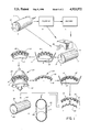
- FIG. 1 is a diagrammatic flow chart illustrating the various steps in producing a cylindrical embossing tool in accordance with one preferred embodiment of the present invention.
- FIG. 2 is a perspective view of a preferred stamping tool for use in accordance with the invention in its initial stage.
- FIG. 3 is a perspective view of the preferred stamping tool of FIG. 2 showing the undercutting thereof.
- FIG. 4 is a side view of the preferred stamping tool showing its condition after undercutting.
- FIG. 5 is a side view of the finished preferred stamping tool for use in accordance with the invention.
- Step A a coating or a seamless layer of an embossable material 11 of a polymeric or plastic material is placed as a sleeve snugly around a rigid, such as a steel, cylinder 12.
- the length and circumference of rigid cylinder 12 can be varied to produce a final image transfer or embossing tool of a desired size which will depend upon the image to be replicated and the size of the web material to be embossed.
- the embossable material can be a polymer material or a thermoplastic material such as, for example, polyesters, polystyrenes, ABS copolymers, acrylics and the like.
- the thickness of the embossable layer 11 can vary, but is generally and preferably of a thickness of about 1/8 to 1/2 inch.
- Placement of the seamless layer of embossable material onto the cylinder can be accomplished in a variety of ways.
- a thin wall tube of acrylic material of a size which permits it to slip over the cylinder can be used. Heating the acrylic one or more times to a temperature of about 190° F. and permitting it to cool causes the acrylic to shrink over the exterior of said cylinder. The acrylic tube can then be machined and polished to the desired size.
- a seamless layer of embossable material can be placed on the rigid cylinder by dipping the cylinder into a bath of a polymeric resin and permitting the resin to cure and form a layer on the cylinder. One or more dipping operations can be conducted to provide an embossable layer of desired thickness. If necessary or desired, but preferably, the exposed surface of the embossable material layer 11 is polished in Step B to produce a cylindrical shape having a polished surface.
- Step C a thin layer of a metal such as silver can be deposited on the exposed embossable layer 11 to render it electrically conductive and/or optically reflective.
- Metal deposition at Step C is optional, but is generally beneficial with respect to visual observation of the imaged or patterned surface during the process of manufacture of the embossing tool.
- the metal layer also serves to provide a release interface.
- a stamping operation is conducted at Step D to place a desired image or pattern 14 over the entire exterior surface of the embossable layer 11.
- the stamping operation is conducted using an imaging tool or a stamper 35, the stamping surface of which has a curvature corresponding to the curvature of the embossable layer on rigid cylinder 12.
- a preferred imaging tool will be described in greater detail hereinafter.
- the temperature, load and dwell time used in the stamping operation can be controlled so as to achieve a desired depth of embossment or penetration of the embossable layer 11.
- the degree of penetration of the imaged surface of the stamping tool into the layer is in the range of about 0.0001 to 0.001 inches depending upon the type of image or pattern to be replicated.
- Step E electroforming is carried out in Step E in known manner to form a nickel electroform 16 on the entire outer surface of the embossable material layer 11.
- the thickness of electroform 16 is generally on the order of about 0.010 to 0.070 inch.
- the electroform 16 is an exact negative of the image or pattern which had been stamped on the embossable material layer 11.
- a reinforcement layer 20 is then applied in Step F over the electroform 16.
- the reinforcement layer can be composed of an adhesive, epoxy resin, and a filler material, such as fiberglass particles and the like.
- the reinforcement layer 20 is added to provide greater rigidity and stability and to mask the electroform 16 during a subsequent electroforming operation. This composite is referred to as the image carrier (23) in Step G.
- the rigid cylinder 12 is removed from the image carrier 23.
- the rigid cylinder 12 can be removed by applying force along its center line and slipping it out of the now rigid reinforced image carrier 23 while preventing movement of the carrier 23.
- the image carrier 23 in the shape of a hollow cylinder consists of the embossed layer 11, metal (silver) layer, if employed, (not shown in the drawings), electroform negative image 16 and reinforcement layer 20.
- the embossed layer 11 is stripped from the image carrier 23 at Step H, leaving in the shape of a hollow cylinder a plating mandrel 25 having original electroform 16 as the interior component contained by the exterior reinforcement layer 20.
- Plating mandrel 25 is again electroplated in Step I to deposit an electroform 28 on the interior surface of the plating mandrel 25.
- the electroform 28 having a thickness of about 0.005 to 0.012 inch and a positive image replica of electroform 16 is then, at Step J, removed from the interior of the plating mandrel. This can be readily accomplished by folding its center appropriately to release it from the plating mandrel and to reduce its diameter.
- the imaged electroform 28 suitably carried forms an embossing tool which can be used to emboss webs of embossable materials in continuous manner.
- the electroform 28 can be placed over a metal carrier cylinder such as an aluminum cylinder 29 having an outer diameter so as to fit snugly within the electroform imaged sleeve 28.
- the imaged sleeve 28 can be placed over carrier cylinder 29 by introducing air into the interface of the two and then floating the imaged sleeve into its position to form a supported embossing tool 30.
- the imaged electroform 28 can be carried by a plurality of rollers 31 to form an endless belt 32 embossing tool.
- the embossing tools 30 and 32 comprising the imaged electroform 28 and a carrier therefor are now ready for use to emboss webs of embossable materials in a continuous manner.
- the embossing tool can be used to transfer images or patterns such as digitally encoded audio and/or video information, to a web of thermoplastic material as described in copending application Ser. No. 887,902, now U.S. Pat. No. 4,190,893, or in other known web embossing methods.
- the imaged electroform embossing tool 28 can be used advantageously to replicate surface images or patterns such as holograms, diffraction gratings, decorative images and the like.
- the plating mandrel 25 can be returned to Step I for electroplating again. In this way, a plurality of embossing tools can be produced.
- Important features of the present invention involve stamping the image or pattern which is to be replicated directly onto a curved cylindrical surface so as to avoid the necessity of stamping an image or pattern to be replicated on a planar surface and then converting to a cylindrical shape.
- gaps or seams are inherently produced in the replications because to do so requires that a plurality of planar images be assembled to make cylindrical segments which are nested together to form a completed cylindrical surface. The size of the gaps depends upon the ability to nest together the segments. However, for images and surface patterns viewed by the human eye discontinuities are noticeable in the assembly.
- the image or pattern to be replicated is stamped directly onto a curved cylindrical surface.
- an imaging tool or stamper 35 having a curved stamping surface is used for the stamping operation.
- a preferred form of the stamper is illustrated in FIGS. 2-5.
- FIG. 2 shows a tool 35 which is machined from a nickel electroform having a curved bottom surface 36 carrying an image or pattern 14 which is to be replicated.
- This imaged bottom surface 36 is not flat, but rather is curved and has a radius of curvature matching that of the embossable material layer 11 which is to be imaged.
- the size of the stamper 35 can be varied as desired depending on the image or pattern which is to be replicated. Machining of the nickel imaging tool 35 generally leaves a small flaw at the bottom edge of the tool in the form of a minute burr 37 next to the image. This burr 37 extends around the entire perimeter of the stamping tool. If this burr were not removed before imaging, a slight, but noticeable, seam of "optically dead” area would surround each stamp.
- the tool edge is undercut as at 38 as shown in FIGS. 3, 4 and 5.
- the undercut 38 leaves a small overhang 39 at the edge of the tool which extends approximately 0.050 of an inch (FIG. 4).
- Undercutting of the tool edge weakens its perimeter along the undercut.
- the stamping tool is then stressed to bend the overhanging edge of the stamper slightly upward into a more horizontal plane as shown in FIG. 5. Bending of the overhang edge portion 39 upwardly can be accomplished by heating the stamper to a temperature on the order of 250° F. and stamping the embossable material layer 11 with an excessive pressure so as to bend the stamping tool edge 39 very slightly upwardly. This stressing or edge bending operation does not in any way harm the integrity of the image on the tool.
- each stamp has a gentle fading of the image on the cylinder surface.
- overlapping of the stampings provides a smooth transition from one stamping to the next so that the entire stamped surface is optically active.
Abstract
Description
Claims (15)
Priority Applications (4)
| Application Number | Priority Date | Filing Date | Title |
|---|---|---|---|
| US07/251,174 US4923572A (en) | 1988-09-29 | 1988-09-29 | Image transfer tool |
| GB8921623A GB2224470A (en) | 1988-09-29 | 1989-09-25 | Image transfer tool. |
| DE3932198A DE3932198A1 (en) | 1988-09-29 | 1989-09-27 | IMPRESSION TOOL AND METHOD FOR THE PRODUCTION THEREOF |
| JP1250818A JPH02134229A (en) | 1988-09-29 | 1989-09-28 | Picture transfer tool |
Applications Claiming Priority (1)
| Application Number | Priority Date | Filing Date | Title |
|---|---|---|---|
| US07/251,174 US4923572A (en) | 1988-09-29 | 1988-09-29 | Image transfer tool |
Publications (1)
| Publication Number | Publication Date |
|---|---|
| US4923572A true US4923572A (en) | 1990-05-08 |
Family
ID=22950807
Family Applications (1)
| Application Number | Title | Priority Date | Filing Date |
|---|---|---|---|
| US07/251,174 Expired - Fee Related US4923572A (en) | 1988-09-29 | 1988-09-29 | Image transfer tool |
Country Status (4)
| Country | Link |
|---|---|
| US (1) | US4923572A (en) |
| JP (1) | JPH02134229A (en) |
| DE (1) | DE3932198A1 (en) |
| GB (1) | GB2224470A (en) |
Cited By (38)
| Publication number | Priority date | Publication date | Assignee | Title |
|---|---|---|---|---|
| US5109589A (en) * | 1991-03-11 | 1992-05-05 | United Technologies Corporation | Processes for making metal prototype parts |
| US5327825A (en) * | 1993-05-12 | 1994-07-12 | Transfer Print Foils, Inc. | Seamless holographic transfer |
| WO1995022448A2 (en) * | 1994-02-17 | 1995-08-24 | Imperial Chemical Industries Plc | Preparation of embossing shims |
| US5521030A (en) * | 1990-07-20 | 1996-05-28 | Mcgrew; Stephen P. | Process for making holographic embossing tools |
| WO1998011472A1 (en) * | 1996-09-11 | 1998-03-19 | Raul Maria Orlandi | System for regional etching of holographic microetchings, diffraction gratings, kinograms, pixelgrams or other optical elements on sheets |
| US5932150A (en) * | 1997-08-25 | 1999-08-03 | Holo-Source Corporation | Replication of diffraction images in oriented films |
| US6222157B1 (en) | 1998-04-17 | 2001-04-24 | L.A. Batchelder And Sons Consulting, Inc. | Seamless holographic transfer using laser generated optical effect patterns |
| US20040009405A1 (en) * | 2002-07-09 | 2004-01-15 | Cheng-Hsiu Chen | Hologram media printing wheel |
| US20040031404A1 (en) * | 2002-08-19 | 2004-02-19 | John Dixon | Seamless embossing shim |
| US20040099395A1 (en) * | 2000-09-07 | 2004-05-27 | Wang San Zhuang | Seamless master and method of making same |
| US20050239935A1 (en) * | 2004-04-26 | 2005-10-27 | Kang Gary Y | Roll-to-roll embossing tools and processes |
| US20060127646A1 (en) * | 2003-01-13 | 2006-06-15 | Kunstoff-Technik Scherer & Trier Gmbh & Co Kg | Laminated decorative strip and method for producing a laminated decorative strip |
| US20070042129A1 (en) * | 2005-08-22 | 2007-02-22 | Kang Gary Y | Embossing assembly and methods of preparation |
| US20070125651A1 (en) * | 2005-12-02 | 2007-06-07 | Buckley Paul W | Electroform, methods of making electroforms, and products made from electroforms |
| US20070125654A1 (en) * | 2005-12-02 | 2007-06-07 | Buckley Paul W | Electroform, methods of making electroforms, and products made from electroforms |
| US20070126148A1 (en) * | 2005-12-02 | 2007-06-07 | General Electric Company | Microstructured embossing drum and articles made therefrom |
| US20070125248A1 (en) * | 2005-12-02 | 2007-06-07 | Coyle Dennis J | Embossing drum system with removable outer sleeve and methods of use |
| US20070125655A1 (en) * | 2005-12-02 | 2007-06-07 | Buckley Paul W | Electroform, methods of making electroforms, and products made from electroforms |
| US20070125652A1 (en) * | 2005-12-02 | 2007-06-07 | Buckley Paul W | Electroform, methods of making electroforms, and products made from electroforms |
| US20070204953A1 (en) * | 2006-02-21 | 2007-09-06 | Ching-Bin Lin | Method for forming structured film as molded by tape die |
| EP1999513A1 (en) * | 2006-03-28 | 2008-12-10 | LG Chem. Ltd. | Method of forming nanopattern and substrate having pattern formed using the method |
| US20080311235A1 (en) * | 2005-01-21 | 2008-12-18 | Slafer Dennis W | Replication Tools and Related Fabrication Methods and Apparatus |
| US20090130607A1 (en) * | 2004-01-21 | 2009-05-21 | Microcontinuum, Inc | Roll-to-roll patterning of transparent and metallic layers |
| US20100116156A1 (en) * | 2008-11-10 | 2010-05-13 | Illinois Tool Works Inc. | Multi-axis diffraction grating |
| US7833389B1 (en) * | 2005-01-21 | 2010-11-16 | Microcontinuum, Inc. | Replication tools and related fabrication methods and apparatus |
| US20100319433A1 (en) * | 2006-12-07 | 2010-12-23 | Stanley Walter Vigurs | Process for producing a die |
| US20110012285A1 (en) * | 2008-03-14 | 2011-01-20 | Dong-Seob Kim | Method for fabricating 3d structure having hydrophobic surface using metal foil |
| US20110089604A1 (en) * | 2009-05-08 | 2011-04-21 | Hoowaki, Llc | Method of manufacturing products having a metal surface |
| US20110156295A1 (en) * | 2009-12-24 | 2011-06-30 | Hon Hai Precision Industry Co., Ltd. | Embossing assembly, manufacturing method thereof, and embossing method using the same |
| US20130052294A1 (en) * | 2011-03-30 | 2013-02-28 | Taiwan Green Point Enterprises Co., Ltd. | Molding tool with a three dimensional surface relief pattern and method of making the same |
| US20140232037A1 (en) * | 2011-12-06 | 2014-08-21 | Ev Group E. Thallner Gmbh | Nanostructure die, embossing roll, device and method for continuous embossing of nanostructures |
| US20150114062A1 (en) * | 2010-02-06 | 2015-04-30 | Illinois Tool Works Inc. | Seamless sleeve and seamless substrate |
| US20160067890A1 (en) * | 2012-02-16 | 2016-03-10 | Sumitomo Rubber Industries, Ltd. | Sheet conveying roller and production method thereof |
| WO2019145118A1 (en) * | 2018-01-29 | 2019-08-01 | Giesecke+Devrient Currency Technology Gmbh | Embossing plate for producing embossed structures in a valuable object and methods for producing an embossing plate |
| US10682805B2 (en) | 2006-02-27 | 2020-06-16 | Microcontinuum, Inc. | Formation of pattern replicating tools |
| US10879595B2 (en) | 2013-05-17 | 2020-12-29 | Microcontinuum, Inc. | Tools and methods for producing nanoantenna electronic devices |
| US20220016866A1 (en) * | 2020-07-16 | 2022-01-20 | Bixby International Corporation | Micro Embossing |
| CN115125589A (en) * | 2022-07-21 | 2022-09-30 | 北京工业大学 | Low-cost manufacturing method of large-area nano-structure roller die |
Families Citing this family (9)
| Publication number | Priority date | Publication date | Assignee | Title |
|---|---|---|---|---|
| JPH05214577A (en) * | 1992-01-30 | 1993-08-24 | Think Lab Kk | Manufacture of embossing pattern plate |
| DE4302472C2 (en) * | 1993-01-29 | 1996-07-25 | Horst Sitte Heispraegetechnik | Embossing tool |
| DE19780654B4 (en) * | 1996-07-09 | 2004-08-26 | Giesecke & Devrient Gmbh | Embossed form making process - involves making embossing stamp, preparing cylindrical intermediate form, using stamp on regions of it, metallising cylinder surface and removing metal layer |
| DE19627638A1 (en) * | 1996-07-09 | 1998-01-15 | Giesecke & Devrient Gmbh | Stamping cylinder for the production of stamping foils |
| DE10225615A1 (en) * | 2002-06-07 | 2003-12-18 | Giesecke & Devrient Gmbh | Stamping cylinders for the production of stamping foils |
| DE102004050984B3 (en) * | 2004-10-20 | 2006-07-06 | Hueck Folien Gmbh & Co. Kg | Method of making an endless nickel die for embossing textured surfaces |
| EP2164703B1 (en) * | 2007-06-28 | 2018-09-12 | Emot Co., Ltd | Method of duplicating nano-scaled pattern texture on object's surface by imprinting and electroforming |
| CN102107563A (en) * | 2009-12-25 | 2011-06-29 | 鸿富锦精密工业(深圳)有限公司 | Imprinting component, manufacturing method thereof and method for forming brightness enhancement film |
| CN102107564A (en) * | 2009-12-25 | 2011-06-29 | 鸿富锦精密工业(深圳)有限公司 | Impressing component, preparation method thereof and impressing forming method of light guide plate |
Citations (4)
| Publication number | Priority date | Publication date | Assignee | Title |
|---|---|---|---|---|
| US2749294A (en) * | 1952-02-19 | 1956-06-05 | Hedwin Corp | Method of making molds for thermoplastics |
| US3565978A (en) * | 1967-09-11 | 1971-02-23 | Xerox Corp | Replication of surface deformation images |
| US4478769A (en) * | 1982-09-30 | 1984-10-23 | Amerace Corporation | Method for forming an embossing tool with an optically precise pattern |
| US4486363A (en) * | 1982-09-30 | 1984-12-04 | Amerace Corporation | Method and apparatus for embossing a precision optical pattern in a resinous sheet |
-
1988
- 1988-09-29 US US07/251,174 patent/US4923572A/en not_active Expired - Fee Related
-
1989
- 1989-09-25 GB GB8921623A patent/GB2224470A/en not_active Withdrawn
- 1989-09-27 DE DE3932198A patent/DE3932198A1/en not_active Withdrawn
- 1989-09-28 JP JP1250818A patent/JPH02134229A/en active Pending
Patent Citations (4)
| Publication number | Priority date | Publication date | Assignee | Title |
|---|---|---|---|---|
| US2749294A (en) * | 1952-02-19 | 1956-06-05 | Hedwin Corp | Method of making molds for thermoplastics |
| US3565978A (en) * | 1967-09-11 | 1971-02-23 | Xerox Corp | Replication of surface deformation images |
| US4478769A (en) * | 1982-09-30 | 1984-10-23 | Amerace Corporation | Method for forming an embossing tool with an optically precise pattern |
| US4486363A (en) * | 1982-09-30 | 1984-12-04 | Amerace Corporation | Method and apparatus for embossing a precision optical pattern in a resinous sheet |
Cited By (65)
| Publication number | Priority date | Publication date | Assignee | Title |
|---|---|---|---|---|
| US5521030A (en) * | 1990-07-20 | 1996-05-28 | Mcgrew; Stephen P. | Process for making holographic embossing tools |
| US5109589A (en) * | 1991-03-11 | 1992-05-05 | United Technologies Corporation | Processes for making metal prototype parts |
| US5327825A (en) * | 1993-05-12 | 1994-07-12 | Transfer Print Foils, Inc. | Seamless holographic transfer |
| WO1995022448A2 (en) * | 1994-02-17 | 1995-08-24 | Imperial Chemical Industries Plc | Preparation of embossing shims |
| WO1995022448A3 (en) * | 1994-02-17 | 1995-10-05 | Ici Plc | Preparation of embossing shims |
| WO1998011472A1 (en) * | 1996-09-11 | 1998-03-19 | Raul Maria Orlandi | System for regional etching of holographic microetchings, diffraction gratings, kinograms, pixelgrams or other optical elements on sheets |
| US5932150A (en) * | 1997-08-25 | 1999-08-03 | Holo-Source Corporation | Replication of diffraction images in oriented films |
| US6222157B1 (en) | 1998-04-17 | 2001-04-24 | L.A. Batchelder And Sons Consulting, Inc. | Seamless holographic transfer using laser generated optical effect patterns |
| US20040099395A1 (en) * | 2000-09-07 | 2004-05-27 | Wang San Zhuang | Seamless master and method of making same |
| US8097311B2 (en) * | 2000-09-07 | 2012-01-17 | Asahi Kasei Kabushiki Kaisha | Seamless master and method of making same |
| US20040009405A1 (en) * | 2002-07-09 | 2004-01-15 | Cheng-Hsiu Chen | Hologram media printing wheel |
| WO2004016830A1 (en) * | 2002-08-19 | 2004-02-26 | Holman Technology, Inc. | Seamless embossing shim |
| US20050082699A1 (en) * | 2002-08-19 | 2005-04-21 | John Dixon | Seamless embossing shim |
| US20040031404A1 (en) * | 2002-08-19 | 2004-02-19 | John Dixon | Seamless embossing shim |
| US20100021705A1 (en) * | 2003-01-13 | 2010-01-28 | Kunststoff-Technik Scherer & Trier Gmbh & Co Kg | Laminated Decorative Strip and Method for the Producion of a Laminated Decorative Strip |
| US8968826B2 (en) | 2003-01-13 | 2015-03-03 | Kunststoff-Technik Scherer & Trier Gmbh & Co Kg | Laminated decorative strip and method for producing a laminated decorative strip |
| US20060127646A1 (en) * | 2003-01-13 | 2006-06-15 | Kunstoff-Technik Scherer & Trier Gmbh & Co Kg | Laminated decorative strip and method for producing a laminated decorative strip |
| US10546722B2 (en) | 2004-01-21 | 2020-01-28 | Microcontinuum, Inc. | Roll-to-roll patterning of transparent and metallic layers |
| US9307648B2 (en) | 2004-01-21 | 2016-04-05 | Microcontinuum, Inc. | Roll-to-roll patterning of transparent and metallic layers |
| US20090130607A1 (en) * | 2004-01-21 | 2009-05-21 | Microcontinuum, Inc | Roll-to-roll patterning of transparent and metallic layers |
| WO2005103134A3 (en) * | 2004-04-26 | 2007-04-12 | Sipix Imaging Inc | Roll-to-roll embossing tools and processes |
| WO2005103134A2 (en) * | 2004-04-26 | 2005-11-03 | Sipix Imaging, Inc. | Roll-to-roll embossing tools and processes |
| US7470386B2 (en) | 2004-04-26 | 2008-12-30 | Sipix Imaging, Inc. | Roll-to-roll embossing tools and processes |
| US20050239935A1 (en) * | 2004-04-26 | 2005-10-27 | Kang Gary Y | Roll-to-roll embossing tools and processes |
| US8062495B2 (en) | 2005-01-21 | 2011-11-22 | Microcontinuum, Inc. | Replication tools and related fabrication methods and apparatus |
| US9395623B2 (en) | 2005-01-21 | 2016-07-19 | Microcontinuum, Inc. | Replication tools and related fabrication methods and apparatus |
| US10546607B2 (en) | 2005-01-21 | 2020-01-28 | Microcontinuum, Inc. | Replication tools and related fabrication methods and apparatus |
| US20110064838A1 (en) * | 2005-01-21 | 2011-03-17 | Microcontinuum, Inc. | Replication tools and related fabrication methos and apparatus |
| US7833389B1 (en) * | 2005-01-21 | 2010-11-16 | Microcontinuum, Inc. | Replication tools and related fabrication methods and apparatus |
| US20080311235A1 (en) * | 2005-01-21 | 2008-12-18 | Slafer Dennis W | Replication Tools and Related Fabrication Methods and Apparatus |
| US7767126B2 (en) | 2005-08-22 | 2010-08-03 | Sipix Imaging, Inc. | Embossing assembly and methods of preparation |
| US20070042129A1 (en) * | 2005-08-22 | 2007-02-22 | Kang Gary Y | Embossing assembly and methods of preparation |
| US20070126148A1 (en) * | 2005-12-02 | 2007-06-07 | General Electric Company | Microstructured embossing drum and articles made therefrom |
| US20070125651A1 (en) * | 2005-12-02 | 2007-06-07 | Buckley Paul W | Electroform, methods of making electroforms, and products made from electroforms |
| US20070125654A1 (en) * | 2005-12-02 | 2007-06-07 | Buckley Paul W | Electroform, methods of making electroforms, and products made from electroforms |
| US20070125248A1 (en) * | 2005-12-02 | 2007-06-07 | Coyle Dennis J | Embossing drum system with removable outer sleeve and methods of use |
| US20070125655A1 (en) * | 2005-12-02 | 2007-06-07 | Buckley Paul W | Electroform, methods of making electroforms, and products made from electroforms |
| US20070125652A1 (en) * | 2005-12-02 | 2007-06-07 | Buckley Paul W | Electroform, methods of making electroforms, and products made from electroforms |
| US20070204953A1 (en) * | 2006-02-21 | 2007-09-06 | Ching-Bin Lin | Method for forming structured film as molded by tape die |
| US10682805B2 (en) | 2006-02-27 | 2020-06-16 | Microcontinuum, Inc. | Formation of pattern replicating tools |
| EP1999513A4 (en) * | 2006-03-28 | 2010-03-10 | Lg Chemical Ltd | Method of forming nanopattern and substrate having pattern formed using the method |
| EP1999513A1 (en) * | 2006-03-28 | 2008-12-10 | LG Chem. Ltd. | Method of forming nanopattern and substrate having pattern formed using the method |
| US20100319433A1 (en) * | 2006-12-07 | 2010-12-23 | Stanley Walter Vigurs | Process for producing a die |
| US8459086B2 (en) * | 2006-12-07 | 2013-06-11 | UEI Fine Cut Limited | Process for producing a die |
| US20110012285A1 (en) * | 2008-03-14 | 2011-01-20 | Dong-Seob Kim | Method for fabricating 3d structure having hydrophobic surface using metal foil |
| US8257630B2 (en) * | 2008-03-14 | 2012-09-04 | Postech Academy-Industry Foundation | Method for fabricating 3D structure having hydrophobic surface using metal foil |
| US20100116156A1 (en) * | 2008-11-10 | 2010-05-13 | Illinois Tool Works Inc. | Multi-axis diffraction grating |
| WO2010054329A1 (en) * | 2008-11-10 | 2010-05-14 | Illinois Tool Works Inc. | Improved multi-axis diffraction grating |
| CN102197345A (en) * | 2008-11-10 | 2011-09-21 | 伊利诺斯工具制品有限公司 | Improved multi-axis diffraction grating |
| CN102197345B (en) * | 2008-11-10 | 2017-08-18 | 伊利诺斯工具制品有限公司 | improved multi-axis diffraction grating |
| US20110089604A1 (en) * | 2009-05-08 | 2011-04-21 | Hoowaki, Llc | Method of manufacturing products having a metal surface |
| US8814954B2 (en) * | 2009-05-08 | 2014-08-26 | Hoowaki, Llc | Method of manufacturing products having a metal surface |
| US20110156295A1 (en) * | 2009-12-24 | 2011-06-30 | Hon Hai Precision Industry Co., Ltd. | Embossing assembly, manufacturing method thereof, and embossing method using the same |
| US10265745B2 (en) * | 2010-02-06 | 2019-04-23 | Illinois Tool Works Inc. | Seamless sleeve and seamless substrate |
| US20150114062A1 (en) * | 2010-02-06 | 2015-04-30 | Illinois Tool Works Inc. | Seamless sleeve and seamless substrate |
| US20130052294A1 (en) * | 2011-03-30 | 2013-02-28 | Taiwan Green Point Enterprises Co., Ltd. | Molding tool with a three dimensional surface relief pattern and method of making the same |
| US9764511B2 (en) * | 2011-12-06 | 2017-09-19 | Ev Group E. Thallner Gmbh | Nanostructure die, embossing roll, device and method for continuous embossing of nanostructures |
| US20140232037A1 (en) * | 2011-12-06 | 2014-08-21 | Ev Group E. Thallner Gmbh | Nanostructure die, embossing roll, device and method for continuous embossing of nanostructures |
| US10099405B2 (en) * | 2012-02-16 | 2018-10-16 | Sumitomo Rubber Industries, Ltd. | Sheet conveying roller and production method therefor |
| US20160067890A1 (en) * | 2012-02-16 | 2016-03-10 | Sumitomo Rubber Industries, Ltd. | Sheet conveying roller and production method thereof |
| US10879595B2 (en) | 2013-05-17 | 2020-12-29 | Microcontinuum, Inc. | Tools and methods for producing nanoantenna electronic devices |
| WO2019145118A1 (en) * | 2018-01-29 | 2019-08-01 | Giesecke+Devrient Currency Technology Gmbh | Embossing plate for producing embossed structures in a valuable object and methods for producing an embossing plate |
| US20220016866A1 (en) * | 2020-07-16 | 2022-01-20 | Bixby International Corporation | Micro Embossing |
| CN115125589A (en) * | 2022-07-21 | 2022-09-30 | 北京工业大学 | Low-cost manufacturing method of large-area nano-structure roller die |
| CN115125589B (en) * | 2022-07-21 | 2024-03-08 | 北京工业大学 | Low-cost manufacturing method of large-area nano-structure roller die |
Also Published As
| Publication number | Publication date |
|---|---|
| GB8921623D0 (en) | 1989-11-08 |
| JPH02134229A (en) | 1990-05-23 |
| GB2224470A (en) | 1990-05-09 |
| DE3932198A1 (en) | 1990-04-05 |
Similar Documents
| Publication | Publication Date | Title |
|---|---|---|
| US4923572A (en) | Image transfer tool | |
| US5327825A (en) | Seamless holographic transfer | |
| US5071597A (en) | Plastic molding of articles including a hologram or other microstructure | |
| US5521030A (en) | Process for making holographic embossing tools | |
| CA2094813C (en) | Embossing rolls | |
| US4250135A (en) | Roller for producing continuous sueded or grit type finish and method of making | |
| JPH0460815B2 (en) | ||
| JP2002508539A (en) | Method of transferring holographic image to metal surface | |
| US6099289A (en) | Forming mold cavities | |
| US3548041A (en) | Lens mold making by plating lenticulations on a masked conductive support | |
| US20040031404A1 (en) | Seamless embossing shim | |
| WO1991001225A1 (en) | Embossing machine roller | |
| US4705471A (en) | Mold for producing a plate | |
| EP1017553B1 (en) | Forming mold cavities | |
| US5183551A (en) | Method for making a continous metal band having surface impressions | |
| US4987799A (en) | Stamping die replica and method of manufacture thereof | |
| JP2002200900A (en) | Can with three-dimensional hologram | |
| JP2789599B2 (en) | Method of manufacturing hologram surface-mounted mold | |
| JPH057265B2 (en) | ||
| JPH0454238B2 (en) | ||
| JPS63178015A (en) | Genuine woodgrained resin molded item and manufacture thereof | |
| JPH0370507A (en) | Metallic ornament with fingerprint and manufacture thereof | |
| JPH0541748B2 (en) | ||
| KR100939090B1 (en) | Manufacturing method of electro forming mold for mass production of electro forming products using uv pattern transfer | |
| CN1084448A (en) | Copying hologram and grating technology on crust |
Legal Events
| Date | Code | Title | Description |
|---|---|---|---|
| AS | Assignment |
Owner name: HALLMARK CARDS, INCORPORATED, 2500 MCGEE TRAFFICWA Free format text: ASSIGNMENT OF ASSIGNORS INTEREST.;ASSIGNORS:WATKINS, JOHN;MAGEE, RAMON;DOERFLINGER, ARTHUR;REEL/FRAME:004957/0407 Effective date: 19880922 Owner name: HALLMARK CARDS, INCORPORATED, A CORP. OF MO,MISSOU Free format text: ASSIGNMENT OF ASSIGNORS INTEREST;ASSIGNORS:WATKINS, JOHN;MAGEE, RAMON;DOERFLINGER, ARTHUR;REEL/FRAME:004957/0407 Effective date: 19880922 |
|
| CC | Certificate of correction | ||
| FEPP | Fee payment procedure |
Free format text: PAYOR NUMBER ASSIGNED (ORIGINAL EVENT CODE: ASPN); ENTITY STATUS OF PATENT OWNER: LARGE ENTITY |
|
| FPAY | Fee payment |
Year of fee payment: 4 |
|
| FEPP | Fee payment procedure |
Free format text: PAYOR NUMBER ASSIGNED (ORIGINAL EVENT CODE: ASPN); ENTITY STATUS OF PATENT OWNER: LARGE ENTITY Free format text: PAYER NUMBER DE-ASSIGNED (ORIGINAL EVENT CODE: RMPN); ENTITY STATUS OF PATENT OWNER: LARGE ENTITY |
|
| REMI | Maintenance fee reminder mailed | ||
| LAPS | Lapse for failure to pay maintenance fees | ||
| STCH | Information on status: patent discontinuation |
Free format text: PATENT EXPIRED DUE TO NONPAYMENT OF MAINTENANCE FEES UNDER 37 CFR 1.362 |
|
| FP | Lapsed due to failure to pay maintenance fee |
Effective date: 20020508 |
|
| AS | Assignment |
Owner name: STERLING NATIONAL BANK, NEW YORK Free format text: SECURITY AGREEMENT;ASSIGNOR:UNIFOIL CORPORATION;REEL/FRAME:013081/0124 Effective date: 20020620 |