US4866651A - Method and circuit arrangement for adding floating point numbers - Google Patents
Method and circuit arrangement for adding floating point numbers Download PDFInfo
- Publication number
- US4866651A US4866651A US07/089,649 US8964987A US4866651A US 4866651 A US4866651 A US 4866651A US 8964987 A US8964987 A US 8964987A US 4866651 A US4866651 A US 4866651A
- Authority
- US
- United States
- Prior art keywords
- remainder
- input
- sum
- stage
- adder
- Prior art date
- Legal status (The legal status is an assumption and is not a legal conclusion. Google has not performed a legal analysis and makes no representation as to the accuracy of the status listed.)
- Expired - Fee Related
Links
Images
Classifications
-
- G—PHYSICS
- G06—COMPUTING; CALCULATING OR COUNTING
- G06F—ELECTRIC DIGITAL DATA PROCESSING
- G06F7/00—Methods or arrangements for processing data by operating upon the order or content of the data handled
- G06F7/38—Methods or arrangements for performing computations using exclusively denominational number representation, e.g. using binary, ternary, decimal representation
- G06F7/48—Methods or arrangements for performing computations using exclusively denominational number representation, e.g. using binary, ternary, decimal representation using non-contact-making devices, e.g. tube, solid state device; using unspecified devices
- G06F7/483—Computations with numbers represented by a non-linear combination of denominational numbers, e.g. rational numbers, logarithmic number system or floating-point numbers
- G06F7/485—Adding; Subtracting
Definitions
- This invention generally relates to mechanisms for performing the addition of numbers stored in "floating point" form.
- this invention relates to methods and circuitry for performing floating point addition with minimum loss of precision.
- the smaller number For adding two floating point numbers, the smaller number must be right-shifted until the exponents of both numbers are equal.
- the part of the smaller operand not considered during the addition and which after having been shifted out of the predetermined word length may be referred to as remainder is generally either discarded or considered by rounding the least-significant sum digit. This is described, for example, in IBM TDB October 1969, page 683 and IBM TDB October 1984, pages 3138 to 3140.
- the invention is based on the truncation of the remainder of the smaller operand and its output in normalized floating point notation. This permits processing the remainder in the same floating point adder stages as are used to obtain the mantissa sum of two operands and standardizing the means employed for this purpose, which is favourable for large-scale semiconductor integration. In addition, remainders are immediately processed, leading to time savings.
- the invention is well suited for existing computer structures. Even for very large exponent ranges, say, about ⁇ 5000, as are specified in recent computing standards, the present invention requires only few means, as it is not necessary to provide computer and storage means for the full exponent range straight away, their exact number rather depending on the actual problem to be solved. This leads to a high degree of flexibility, since the storage and computer means are connected as required.
- the adders used according to the invention have a single length mantissa and thus permit high-speed carry operations.
- the parallel operation of the present invention which provides for the adder stages to be series-connected in pipeline form, permits high speeds at a large number of operands, as quite a number of add operations may be carried out simultaneously with respect to input operands, intermediate sums and remainders.
- serial operation according to the present invention permits using a simple arrangement comprising a single floating point adder stage. Representation of the sum requires a plurality of storage registers, whose number, being dependent on the respective problem to be solved, is variable. Thus, a reconfiguration of existing equipment is also possible.
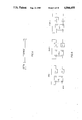
- FIG. 1 shows a data format used in the present description
- FIG. 2 shows a a floating point adder stage, consisting of FIGS. 2A and 2B, with calculation of the remainder,
- FIGS. 3 to 5 show three addition examples in the form of tables
- FIG. 6 shows a series connection of floating point adder stages according to FIG. 2 in pipeline form for parallel operation
- FIG. 7 shows an addition example concerning FIG. 6,
- FIG. 8 shows a circuit arrangement with a single adder stage according to FIG. 2 for serial operation
- FIG. 9 shows an addition example (FIGS. 9A and 9B) explaining the operation of the arrangement of FIG. 8.
- 1.234 is the digit sequence of the mantissa which by definition is assumed to have a digit other than zero before the decimal point.
- E3 indicates that the place before the decimal point has the value 10 3 , i.e., the exponent is 3.
- FIG. 1 shows the data format used in the embodiment described below.
- the 64 bits of the data word are associated as follows:
- Characteristic CH of the mantissa The characteristic is derived from the exponents of the mantissa by addition of the decimal number 64 (hex 40).
- the hexadecimal values of the characteristic of 00 to 40 correspond to a decimal exponent of -64 to 0 and the characteristic values hex 41 to hex 7F to a positive exponent of 1 to 63.
- the mantissa used below has a zero before the decimal point and its first hexidecimal digit after the point must be other than zero.
- FIG. 2 A floating point adder stage according to the invention is shown in FIG. 2 which consists of FIGS. 2A and 2B.
- the numbers in brackets denote the respective bit positions and the numbers in parentheses the number of bits on the respective bus. In some places, this number is also represented by a slash with a number.
- the two summands A and B are fed to one data shift means (DS) 4 and 6 each.
- the characteristics of the two numbers Ch A and Ch B are fed to a characteristic subtracter 2, the output of which emits the characteristic difference and the sign of the subtraction.
- Ch A ⁇ Ch B the two data selectors 4 and 6 are controlled by the sign signal such that summand A is passed by data selector 4 and summand B by data selector 6.
- the two summands are swapped by the data selector, feeding summand B to the upper bus in FIG. 2A and summand A to the lower bus. In this manner, the larger summand invariably reaches the upper bus where it is designated as A".
- the summand on the lower bus is designated as B".
- the mantissa of the smaller number must first be right-shifted such that the two exponents become equal.
- the digits (remainder) thus shifted out of the computer's mantissa width (14 hexadecimal digits) are lost unless further measures are taken for calculation.
- the shift is effected by shift means 8, with the magnitude of shift being controlled by the characteristic difference.
- Shift means 8 is a so-called funnel shifter.
- the input width of the shifter is 2 ⁇ 56 bits and the output width 1 ⁇ 56 bits.
- the right shift produces blank digits at the left end, which, as shown in conjunction with shift means 8, have to be filled with zeros.
- mantissas of the two summands may be added in mantissa adder 10.
- mantissa adder 10 also receives the signs of the two mantissas.
- the sum of the two mantissas which again has 56 bits, a signal denoting a carry, if any, and a sign signal of the sum are emitted at the output of the mantissa adder.
- LZD leading zero detector
- shift means 14 the mantissa is correspondingly left-shifted for normalization. The least-significant places must be filled with zeros, as indicated.
- the characteristic of the sum equals the characteristic of operand A".
- the characteristic of the sum must be modified in characteristic adder 16. At the output of the adder stage, the following signals are emitted with respect to the sum:
- a sum signal S consisting of 64 bits.
- a "sum overflow” signal indicating that the exponent range available has been exceeded and that further calculation without rescaling is impossible.
- a "sum underflow” signal indicating that the negative exponent range has been exceeded.
- a "sum 0" signal indicating that all digits of the sum are 0. By means of this signal, unnecessary operational steps may be skipped.
- the adder stage shown in FIG. 2 may also emit a remainder which similar to FIG. 1 consists of 64 bits.
- a remainder which similar to FIG. 1 consists of 64 bits.
- the mantissas are partly overlapping.
- the overlapping part i.e., the higher digits of the shifted mantissa B" are added to mantissa A", while the remaining lower digits are processed further as a remainder.
- mantissas are not overlapping. In this case, the entire mantissa B" must be truncated as a remainder.
- a shift means 18 is provided according to the invention, which is designed similar to shift means 8 and which truncates the respective least-significant places of mantissa B" as a remainder.
- the remaining places of the truncated mantissa B" must then be filled with zeros, as explained in connection with shift means 18.
- a leading zero detector (LZD) 20, controlling a shift means 22, is also provided for the remaining mantissa.
- the shift operation in shift means 22 depends, in addition to the number of leading zeros, on whether the sum of the two mantissas A" and B" produced a carry.
- the sum mantissa must be right-shifted by one place, as previously explained, so that the least-significant place (bits 60-63) of the sum mantissa is shifted out and entered by shift means 22 into the most-significant place of the remaining mantissa. In this case, the remaining mantissa must be right-shifted by 1 place.
- the least-significant place of the remaining mantissa is always zero, so that right-shifting the remaining mantissa by one place is unproblematical.
- the hexadecimal digit with the bit positions 60-63 shifted out of the sum mantissa at the least-significant place is fed by a gate circuit 24 to shift means 22.
- Gate circuit 24 passes this digit if the sum carry signal is "1".
- the digit shifted out of the sum may be zero, so that the associated 4 bits must also be fed to detector 20.
- the characteristic of the remainder is calculated in the characteristic adder. It is obtained from
- CH R is the characteristic of the remainder
- CH B is the characteristic of the operand B
- SHMT is the shift value emitted by detector 20
- E is the word length of the mantissa, i.e., in the present example 14 hexadecimal digits (hexadecimal E),
- CH D is the characteristic difference emitted by subtracter 2. As the maximum value of this characteristic is assumed to be 14 by definition, i.e., hex. E, 4 lines at the output of subtracter 2 are sufficient.
- SHMT ranges from 1 to -E. and for CHD from 0 to E.
- circuit signal "remainder zero" A significant signal is the circuit signal "remainder zero", as explained in detail further on.
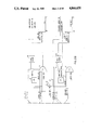
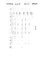
- FIGS. 3 to 5 show three addition examples in the form of tables so that FIG. 2 may be readily appreciated.
- a positive summand B is added to a negative summand A.
- the two operands are represented as hexadecimals digits.
- the two left-most digits of summand A are B4, i.e., 1001 0100.
- the first, left-most, bit denotes the sign. As this bit has the value "1", summand A is negative.
- the remaining 7 bits 011 0100, i.e., 34, represent the characteristic.
- the first two digits of summand B are 40, i.e., 0100 0000.
- the first, left-most, bit is 0, denoting that summand B is positive.
- the characteristic of summand B has the hexadecimal value 40.
- the sign bit at the output of characteristic subtracter 2 is "1", causing the two data selectors 4 and 6 to swap summands.
- Summand A thus becomes summand B" and summand B summand A", as the greater of the two summands is always fed to the upper bus.
- the difference between the two characteristics is C (decimal 12).
- the two least-significant digits of B overlap the two most-significant mantissa digits of A.
- the remaining 12 digits of A are truncated by shift means 18 as a remainder.
- the table also shows the output signals of the remaining units illustrated in FIG. 2. At the end of the table, the signals obtained at output S (for the sum) and R (for the remainder) are shown quite clearly.
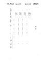
- a positive summand A is added to a negative summand B.
- the mantissas of the two operands are not overlapping.
- the difference between the two characteristics is hexadecimal 10 (decimal 16).
- the characteristic subtracter 2 emits a maximum characteristic difference of E (decimal 14), as the mantissa has only E places.
- this difference value which is too low, is incremented to the correct difference value.
- the entire summand B is emitted as a remainder.
- FIG. 2 The arrangement in FIG. 2 is implemented in purely combinatorial logic. It may also be implemented in sequential logic with buffers and repeated use of significant function groups, such as adders, shift means, etc. This substantially reduces the technical means required but also the processing speed.
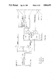
- FIG. 6 shows three series-connected floating point adder stages FPA1 to FPA3. This number has been chosen arbitrarily, which means that more adder stages FPA may be used, if required, with one adder stage corresponding to the arrangement shown in FIG. 2.
- the input of this adder stage receives the summands A and B and its output supplies the sum signal S and the remainder signal R.
- the arrangement of FIG. 6 also comprises a register pair for storing the sum and the remainder signal.
- the operands to be summed are successively applied to the input of the circuit.
- the arrangement of FIG. 6 may be used, for example, for vector operations in which a plurality of operands are successively summed.
- the registers are clocked for the receipt of the fresh value. To avoid instabilities, the registers must either be edge-controlled or be made up of master-slave flip-flops.
- the sum signal generated in the illustrated pipeline arrangement is returned to the A input of the same stage, while the generated remainder signal is fed to the B input of the subsequent stage.
- remainders produced in a particular stage and which cannot be processed therein continue to be shifted in the pipeline arrangement, becoming smaller and smaller. After there are no further operands left, these remainders are processed until finally all remainder registers are zero.
- the "remainder zero" signal of the leading zero detector 20 shown in FIG. 2B thus allows determining the time at which all summands have been summed and the exact result is available in the sum registers.
- the number of floating point adder stages required depends on the respective problem to be solved.
- Tests have shown that a relatively small number of stages are sufficient for solving a high percentage of the arithmetic problems occurring in practice.
- the number of stages required depends on the length of the mantissa and declines with increasing mantissa lengths. For the usual mantissa lengths of 52-56 bits (64 bit word length) 4 to 5 stages are sufficient for most of the problems occurring in practice.
- FIG. 7 shows a computing example in the form of a table so that FIG. 6 may be more readily appreciated. For simplicity, it is assumed that all summands are positive and the digits are in decimal notation. It is assumed that there are four operands to be added
- sum register S1 The result is stored in sum register S1 and the remainder occurring, i.e., the part truncated from operand B supplemented by a zero at the least-significant place in remainder register R1.
- this remainder is fed to input B of stage 2 and, having passed that stage, is stored in sum register S2.
- the third operand is simultaneously added to the content of register S1, which again produces a remainder.
- This remainder is stored in remainder register R1 and fed to input B of stage 2 at clock 4.
- the sum register S2 in stage 2 already contained a value other than zero, an addition is carried out in that stage, storing the result in sum register S1 and the remainder in remainder register R2.
- each new clock causes the value stored in the sum register of a stage to be applied to input A of that stage, while a stored remainder, if any, is applied to input B of the next stage.
- a stored remainder if any, is applied to input B of the next stage.
- the arithmetic operation terminates at clock 7; no further operands are applied and all remainder registers R1 to R4 are zero.
- the "remainder zero" output signal of each adder stage supplies a binary one, which may be readily detected by an AND circuit, and the arithmetic operation terminates. The exact result
- FIG. 8 shows an arrangement with a single adder circuit (FPA) 30, a remainder register 32 and a register stack 34 consisting of several sum registers SMR0-SMRm.
- Input B of the adder circuit may be connected by a changeover switch 36 to an operand input or the output of the remainder register.
- this switch Upon receipt of an operand, this switch is reset, so that subsequently input B is connected to the output of the remainder register.
- the remainder register content is then successively added to the sum register content until finally the remainder register contains only zeros.
- the switch at input B is reset and a fresh operand is applied. After the operand has been received, the switch is reset and addition is repeated until the remainder register contains only zeros. After all operands have been applied, the exact result is available in the sum registers, while the remainder register contains only zeros.
- An example illustrated in FIG. 9 serves to explain this sequence in detail.
- switch 36 connects input B to the operand input, i.e., a fresh operand is applied.
- the next column contains subclocks, if any, to the main clock. At a subclock, the content of remainder registers 32 is added to a storage register SMR. The address of the register concerned is indicated in the next column.
- the next column indicates the value of the operand SMD applied to the operand input.
- the next column contains the value of the operand applied to input B.
- the next column contains the value of the operand applied to input A, which was read from the storage register SMR with the SMR address on the left.
- the next column shows the sum of the two operands A and B.
- the next column shows the content of the remainder register 32. If that content is zero, the next clock is a main clock, i.e., a fresh operand is applied from the operand input.
- the next two columns indicate the address of a storage register SMR and its content.
- the last column denotes the respective computation step.
- the first operand 1,234E12 is applied to input B.
- Input A receives only zeros.
- the sum corresponds to operand B and is stored in register SMR0.
- the next operand 2.345E9
- This addition produces a remainder 3.450E8 which is stored in remainder register 32.
- a subclock has to be introduced which causes the content of the remainder register (at input B) to be added to the content of the next storage register (SMR 1).
- the latter content is zero, so that subsequently the remainder register SMR 1, too, stores only zeros. This reemphasizes how significant it is to detect a zero content in the remainder register and therefore FIG. 8 shows once more the respective output of the adder stage.
- the register stack may also comprise only few registers. Further registers may be added if after storage in the currently last register of the stack there is a remainder other than zero.
- the content of the remainder register is zero and there is no further operand at the operand input, so that the final result is stored in register stack 34 or, more precisely, in registers SMR 0 to SMR 3.
- FIG. 8 shows an address unit (38) which is provided with an address reset input RST which is connected to the "remainder zero" output of adder stage 30.
- the chronological sequence at a main or a subclock is such that initially storage 34 is read and the data are transferred to adder stage 30, and that subsequently the operand input or the remainder register is fed to input B of adder stage 30 and the resulting sum and remainder signals are stored.
- the exact sum determined by the method described is represented by a sequence of floating point numbers. Generally, at that stage the elements of this sequence are not yet ordered according to size, and the mantissas may be overlapping. If the described method is applied to the sequence of floating point numbers thus obtained, the result is an exact sum in which the elements are ordered and the mantissas are non-overlapping.
Landscapes
- Engineering & Computer Science (AREA)
- General Physics & Mathematics (AREA)
- Physics & Mathematics (AREA)
- Mathematical Optimization (AREA)
- Computing Systems (AREA)
- Mathematical Analysis (AREA)
- Computational Mathematics (AREA)
- Pure & Applied Mathematics (AREA)
- Theoretical Computer Science (AREA)
- Nonlinear Science (AREA)
- General Engineering & Computer Science (AREA)
- Complex Calculations (AREA)
- Error Detection And Correction (AREA)
Applications Claiming Priority (2)
| Application Number | Priority Date | Filing Date | Title |
|---|---|---|---|
| EP86115152A EP0265555B1 (de) | 1986-10-31 | 1986-10-31 | Verfahren und Schaltungsanordnung zur Addition von Gleitkommazahlen |
| DE86115152 | 1986-10-31 |
Publications (1)
| Publication Number | Publication Date |
|---|---|
| US4866651A true US4866651A (en) | 1989-09-12 |
Family
ID=8195554
Family Applications (1)
| Application Number | Title | Priority Date | Filing Date |
|---|---|---|---|
| US07/089,649 Expired - Fee Related US4866651A (en) | 1986-10-31 | 1987-08-26 | Method and circuit arrangement for adding floating point numbers |
Country Status (9)
| Country | Link |
|---|---|
| US (1) | US4866651A (ko) |
| EP (1) | EP0265555B1 (ko) |
| JP (1) | JPS63123125A (ko) |
| AT (1) | ATE67619T1 (ko) |
| AU (1) | AU589049B2 (ko) |
| BR (1) | BR8705232A (ko) |
| CA (1) | CA1270955A (ko) |
| DE (1) | DE3681591D1 (ko) |
| ES (1) | ES2026444T3 (ko) |
Cited By (9)
| Publication number | Priority date | Publication date | Assignee | Title |
|---|---|---|---|---|
| US5111421A (en) * | 1990-02-26 | 1992-05-05 | General Electric Company | System for performing addition and subtraction of signed magnitude floating point binary numbers |
| US5268856A (en) * | 1988-06-06 | 1993-12-07 | Applied Intelligent Systems, Inc. | Bit serial floating point parallel processing system and method |
| US5493520A (en) * | 1994-04-15 | 1996-02-20 | International Business Machines Corporation | Two state leading zero/one anticipator (LZA) |
| US5557734A (en) * | 1994-06-17 | 1996-09-17 | Applied Intelligent Systems, Inc. | Cache burst architecture for parallel processing, such as for image processing |
| US5790445A (en) * | 1996-04-30 | 1998-08-04 | International Business Machines Corporation | Method and system for performing a high speed floating point add operation |
| US5880983A (en) * | 1996-03-25 | 1999-03-09 | International Business Machines Corporation | Floating point split multiply/add system which has infinite precision |
| US20070277022A1 (en) * | 2006-05-24 | 2007-11-29 | International Business Machines Corporation | Method, system and program product for establishing decimal floating point operands for facilitating testing of decimal floating point instructions |
| CN105278923A (zh) * | 2015-10-22 | 2016-01-27 | 合肥工业大学 | 一种基于aic信息准则的信号源个数估计硬件电路及其实现方法 |
| US20160139881A1 (en) * | 2014-11-19 | 2016-05-19 | International Business Machines Corporation | Accuracy-conserving floating-point value aggregation |
Families Citing this family (1)
| Publication number | Priority date | Publication date | Assignee | Title |
|---|---|---|---|---|
| JP2693800B2 (ja) * | 1988-12-28 | 1997-12-24 | 甲府日本電気株式会社 | 浮動小数点データ総和演算回路 |
Citations (1)
| Publication number | Priority date | Publication date | Assignee | Title |
|---|---|---|---|---|
| US4644490A (en) * | 1983-04-11 | 1987-02-17 | Hitachi, Ltd. | Floating point data adder |
-
1986
- 1986-10-31 EP EP86115152A patent/EP0265555B1/de not_active Expired - Lifetime
- 1986-10-31 DE DE8686115152T patent/DE3681591D1/de not_active Expired - Fee Related
- 1986-10-31 AT AT86115152T patent/ATE67619T1/de not_active IP Right Cessation
- 1986-10-31 ES ES198686115152T patent/ES2026444T3/es not_active Expired - Lifetime
-
1987
- 1987-08-26 US US07/089,649 patent/US4866651A/en not_active Expired - Fee Related
- 1987-09-18 JP JP62232744A patent/JPS63123125A/ja active Granted
- 1987-10-02 BR BR8705232A patent/BR8705232A/pt not_active IP Right Cessation
- 1987-10-30 CA CA000550740A patent/CA1270955A/en not_active Expired - Fee Related
- 1987-10-30 AU AU80535/87A patent/AU589049B2/en not_active Ceased
Patent Citations (1)
| Publication number | Priority date | Publication date | Assignee | Title |
|---|---|---|---|---|
| US4644490A (en) * | 1983-04-11 | 1987-02-17 | Hitachi, Ltd. | Floating point data adder |
Non-Patent Citations (8)
| Title |
|---|
| Communications of the ACM, vol. 14, No. 11, 11/71, pp. 731 736, New York, U.S., M. A. Malcolm: On Accurate Floating point Summation , paragraph: Extended Summation with Cascading Accumulators. * |
| Communications of the ACM, vol. 14, No. 11, 11/71, pp. 731-736, New York, U.S., M. A. Malcolm: "On Accurate Floating-point Summation", paragraph: Extended Summation with Cascading Accumulators. |
| Communications of the ACM, vol. 7, No. 6, 6/64, pp. 355 356, New York, U.S. J. M. Wolfe: Reducing Truncation Errors by Programming , entire document. * |
| Communications of the ACM, vol. 7, No. 6, 6/64, pp. 355-356, New York, U.S. J. M. Wolfe: "Reducing Truncation Errors by Programming", entire document. |
| IBM Journal of Research and Development, vol. 11, No. 1, 1/67, pp. 34 53, New York, U.S., S. F. Anderson et al.: The IBM System/360 Model 91: Floating point Execution Unit , FIG. 3 and text. * |
| IBM Journal of Research and Development, vol. 11, No. 1, 1/67, pp. 34-53, New York, U.S., S. F. Anderson et al.: "The IBM System/360 Model 91: Floating-point Execution Unit", FIG. 3 and text. |
| Mini Micro Conference Record, 5/84, pp. 10/1(1) 10/1(10), Northeast, New York, U.S.; Nusra Lodhi et al: System Solutions for a High Speed Processor Using Innovative ICs , FIG. 10 and text. * |
| Mini-Micro Conference Record, 5/84, pp. 10/1(1)-10/1(10), Northeast, New York, U.S.; Nusra Lodhi et al: "System Solutions for a High-Speed Processor Using Innovative ICs", FIG. 10 and text. |
Cited By (15)
| Publication number | Priority date | Publication date | Assignee | Title |
|---|---|---|---|---|
| US5268856A (en) * | 1988-06-06 | 1993-12-07 | Applied Intelligent Systems, Inc. | Bit serial floating point parallel processing system and method |
| US5111421A (en) * | 1990-02-26 | 1992-05-05 | General Electric Company | System for performing addition and subtraction of signed magnitude floating point binary numbers |
| US5493520A (en) * | 1994-04-15 | 1996-02-20 | International Business Machines Corporation | Two state leading zero/one anticipator (LZA) |
| US5557734A (en) * | 1994-06-17 | 1996-09-17 | Applied Intelligent Systems, Inc. | Cache burst architecture for parallel processing, such as for image processing |
| US5880983A (en) * | 1996-03-25 | 1999-03-09 | International Business Machines Corporation | Floating point split multiply/add system which has infinite precision |
| US5790445A (en) * | 1996-04-30 | 1998-08-04 | International Business Machines Corporation | Method and system for performing a high speed floating point add operation |
| US20070277022A1 (en) * | 2006-05-24 | 2007-11-29 | International Business Machines Corporation | Method, system and program product for establishing decimal floating point operands for facilitating testing of decimal floating point instructions |
| US7827451B2 (en) | 2006-05-24 | 2010-11-02 | International Business Machines Corporation | Method, system and program product for establishing decimal floating point operands for facilitating testing of decimal floating point instructions |
| US20160139881A1 (en) * | 2014-11-19 | 2016-05-19 | International Business Machines Corporation | Accuracy-conserving floating-point value aggregation |
| US20160139882A1 (en) * | 2014-11-19 | 2016-05-19 | International Business Machines Corporation | Accuracy-conserving floating-point value aggregation |
| US10019227B2 (en) * | 2014-11-19 | 2018-07-10 | International Business Machines Corporation | Accuracy-conserving floating-point value aggregation |
| US10019228B2 (en) * | 2014-11-19 | 2018-07-10 | International Business Machines Corporation | Accuracy-conserving floating-point value aggregation |
| US10540142B2 (en) | 2014-11-19 | 2020-01-21 | International Business Machines Corporation | Accuracy-conserving floating-point value aggregation |
| CN105278923A (zh) * | 2015-10-22 | 2016-01-27 | 合肥工业大学 | 一种基于aic信息准则的信号源个数估计硬件电路及其实现方法 |
| CN105278923B (zh) * | 2015-10-22 | 2017-10-03 | 合肥工业大学 | 一种基于aic信息准则的信号源个数估计硬件电路及其实现方法 |
Also Published As
| Publication number | Publication date |
|---|---|
| EP0265555A1 (de) | 1988-05-04 |
| ES2026444T3 (es) | 1992-05-01 |
| BR8705232A (pt) | 1988-05-24 |
| JPH0568725B2 (ko) | 1993-09-29 |
| AU589049B2 (en) | 1989-09-28 |
| ATE67619T1 (de) | 1991-10-15 |
| DE3681591D1 (de) | 1991-10-24 |
| EP0265555B1 (de) | 1991-09-18 |
| CA1270955A (en) | 1990-06-26 |
| JPS63123125A (ja) | 1988-05-26 |
| AU8053587A (en) | 1988-05-05 |
Similar Documents
| Publication | Publication Date | Title |
|---|---|---|
| US4941120A (en) | Floating point normalization and rounding prediction circuit | |
| US4754421A (en) | Multiple precision multiplication device | |
| US4488252A (en) | Floating point addition architecture | |
| US4700324A (en) | Digital circuit performing an arithmetic operation with an overflow | |
| US4893268A (en) | Circuit and method for accumulating partial products of a single, double or mixed precision multiplication | |
| EP0754998A1 (en) | An arithmetic unit | |
| EP0127988A1 (en) | A normalizing circuit | |
| GB2267589A (en) | Performing integer and floating point division using a single SRT divider | |
| US20180052660A1 (en) | Apparatus and method for fixed point to floating point conversion and negative power of two detector | |
| US4866651A (en) | Method and circuit arrangement for adding floating point numbers | |
| US4276607A (en) | Multiplier circuit which detects and skips over trailing zeros | |
| JPH07168697A (ja) | 倍精度除算回路および方法 | |
| US4639887A (en) | Bifurcated method and apparatus for floating point addition with decreased latency time | |
| EP0416308A2 (en) | Rectangular array signed digit multiplier | |
| US4760550A (en) | Saving cycles in floating point division | |
| EP0063361B1 (en) | Correction circuit for approximate quotient | |
| US3210737A (en) | Electronic data processing | |
| EP0295788A2 (en) | Apparatus and method for an extended arithmetic logic unit for expediting selected operations | |
| US3293418A (en) | High speed divider | |
| US4130879A (en) | Apparatus for performing floating point arithmetic operations using submultiple storage | |
| JPH05250146A (ja) | 整数累乗処理を行なうための回路及び方法 | |
| US4996660A (en) | Selection of divisor multipliers in a floating point divide circuit | |
| US4295202A (en) | Hexadecimal digit shifter output control by a programmable read only memory | |
| US4935890A (en) | Format converting circuit for numeric data | |
| US3508037A (en) | Decimal add/subtract circuitry |
Legal Events
| Date | Code | Title | Description |
|---|---|---|---|
| AS | Assignment |
Owner name: INTERNATIONAL BUSINESS MACHINES CORPORATION, A COR Free format text: ASSIGNMENT OF ASSIGNORS INTEREST.;ASSIGNORS:BLEHER, JOHANNES H.;GERLICHER, AXEL T.;RUMP, SIEGFRIED M.;AND OTHERS;REEL/FRAME:005080/0532;SIGNING DATES FROM 19870925 TO 19890317 |
|
| FPAY | Fee payment |
Year of fee payment: 4 |
|
| FEPP | Fee payment procedure |
Free format text: PAYOR NUMBER ASSIGNED (ORIGINAL EVENT CODE: ASPN); ENTITY STATUS OF PATENT OWNER: LARGE ENTITY |
|
| FPAY | Fee payment |
Year of fee payment: 8 |
|
| FEPP | Fee payment procedure |
Free format text: PAYER NUMBER DE-ASSIGNED (ORIGINAL EVENT CODE: RMPN); ENTITY STATUS OF PATENT OWNER: LARGE ENTITY Free format text: PAYOR NUMBER ASSIGNED (ORIGINAL EVENT CODE: ASPN); ENTITY STATUS OF PATENT OWNER: LARGE ENTITY |
|
| REMI | Maintenance fee reminder mailed | ||
| LAPS | Lapse for failure to pay maintenance fees | ||
| FP | Lapsed due to failure to pay maintenance fee |
Effective date: 20010912 |
|
| STCH | Information on status: patent discontinuation |
Free format text: PATENT EXPIRED DUE TO NONPAYMENT OF MAINTENANCE FEES UNDER 37 CFR 1.362 |