US4851887A - Solid state imager device - Google Patents

Solid state imager device Download PDF

Info

Publication number
US4851887A
US4851887A US07/143,651 US14365188A US4851887A US 4851887 A US4851887 A US 4851887A US 14365188 A US14365188 A US 14365188A US 4851887 A US4851887 A US 4851887A
Authority
US
United States
Prior art keywords
region
charge accumulating
conductivity type
type
solid state
Prior art date
Legal status (The legal status is an assumption and is not a legal conclusion. Google has not performed a legal analysis and makes no representation as to the accuracy of the status listed.)
Expired - Fee Related
Application number
US07/143,651
Inventor
Yoshiaki Hagiwara
Current Assignee (The listed assignees may be inaccurate. Google has not performed a legal analysis and makes no representation or warranty as to the accuracy of the list.)
Sony Corp
Original Assignee
Sony Corp
Priority date (The priority date is an assumption and is not a legal conclusion. Google has not performed a legal analysis and makes no representation as to the accuracy of the date listed.)
Filing date
Publication date
Application filed by Sony Corp filed Critical Sony Corp
Assigned to SONY CORPORATION, A CORP. OF JAPAN reassignment SONY CORPORATION, A CORP. OF JAPAN ASSIGNMENT OF ASSIGNORS INTEREST. Assignors: HAGIWARA, YOSHIAKI
Application granted granted Critical
Publication of US4851887A publication Critical patent/US4851887A/en
Anticipated expiration legal-status Critical
Expired - Fee Related legal-status Critical Current

Links

Images

Classifications

    • HELECTRICITY
    • H01ELECTRIC ELEMENTS
    • H01LSEMICONDUCTOR DEVICES NOT COVERED BY CLASS H10
    • H01L27/00Devices consisting of a plurality of semiconductor or other solid-state components formed in or on a common substrate
    • H01L27/14Devices consisting of a plurality of semiconductor or other solid-state components formed in or on a common substrate including semiconductor components sensitive to infrared radiation, light, electromagnetic radiation of shorter wavelength or corpuscular radiation and specially adapted either for the conversion of the energy of such radiation into electrical energy or for the control of electrical energy by such radiation
    • H01L27/144Devices controlled by radiation
    • H01L27/146Imager structures
    • H01L27/148Charge coupled imagers
    • H01L27/14887Blooming suppression

Definitions

  • This invention relates to a solid state imager device.
  • FIG. 1 there is formed on the surface of a P-type silicon substrate 1 a charge accumulating region 2 made of an N - -type region, an overflow control gate region 3 made of a P-type region adjacent to the charge accumulating region 2, and an overflow drain region 4 made of an N + -type region adjacent to the overflow control region 3.
  • Reference numeral 5 designates a channel stopper region, 6 a charge transfer region made of an N 31 -type region, 7 a transfer electrode made of polycrystalline silicon, and 8 and 9 SiO 2 layers, respectively.
  • the above-mentioned solid state imager device is generally referred to as a lateral overflow-structured solid state imager device.
  • a lateral overflow-structured solid state imager device When excessive signal charges are produced due to the irradiation of intense light, they are drawn out from the charge accumulating region 2 through the overflow control gate region 3 to the overflow drain region 4 and consequently absorbed in the overflow drain region 4. Therefore, the imager device having such structure can satisfactorily remove brooming.
  • solid state imager device of the lateral overflow structure is such that the overflow control gate region 3 and the overflow drain region 4 are juxtaposed adjacent to the charge accumulating region 2 on the surface of the P-type silicon substrate 1, a dimension or area per one pixel is increased by these regions, so that high integration of the imager device cannot be achieved.
  • FIG. 2 There has also been proposed a so-called vertical overflow-structured solid state imager device as shown in FIG. 2.
  • a P-type diffusion region 11 is deposited on the surface of an N-type silicon substrate 10, and the charge accumulating region 2 made of an N 31 -region is formed on the surface of the P-type diffusion region 11.
  • the imager device of such, vertical overflow structure can also satisfactorily remove brooming, similar to the aforementioned that of the lateral overflow structure.
  • the solid state imager device of the vertical overflow structure has difficulty in forming the P-type diffusion region 11, so that its manufacturing process is quite restricted.
  • the present invention provides a solid state imager device having a charge accumulating region of a second conductivity type formed on the surface side of a semiconductor substrate of a first conductivity type, comprising:
  • FIG. 1 is a cross-sectional view showing a main portion of an example of a previously proposed solid state imager device
  • FIG. 2 is a cross-sectional view showing a main portion of another example of a previously proposed solid state imager device
  • FIG. 3 is a cross-sectional view showing a main portion of an embodiment of a solid state imager device according to the present invention
  • FIG. 4 is a top plan view taken along a line IV--IV' of FIG. 3;
  • FIG. 5 is a graph showing the potential level of the respective parts of the solid state imager device shown in FIG. 3;
  • FIGS. 6, 8, 10, 12, 14, 16, 18, 20 and 22 are partial plan views respectively showing a manufacturing process of the solid state imager device shown in FIG. 3;
  • FIG. 7 is a cross-sectional view taken along a line VII--VII' of FIG. 6;
  • FIG. 9 is a cross-sectional view taken along a line IX--IX' of FIG. 8;
  • FIG. 11 is a cross-sectional view taken along a line XI--XI' of FIG. 10;
  • FIG. 13 is a cross-sectional view taken along a line XIII--XIII' of FIG. 12;
  • FIG. 15 is a cross-sectional view taken along a line XV--XV' of FIG. 14;
  • FIG. 17 is a cross-sectional view taken along a line XVII--XVII' of FIG. 16;
  • FIG. 19 is a cross-sectional view taken along a line XIX--XIX' of FIG. 18;
  • FIG. 21 is a cross-sectional view taken along a line XXI--XXI' of FIG. 20.
  • FIG. 23 is a cross-sectional view taken along a line XXIII--XXIII' of FIG. 22;
  • FIGS. 3 to 23 An embodiment of a solid state imager device according to the present invention will hereinafter be described with reference to FIGS. 3 to 23. The description is given to a case where the present invention is applied to a solid state imager device which employs the interline transfer system.
  • the parts in FIGS. 3-23 corresponding to those in FIGS. 1 and 2 are designated by the same reference numerals.
  • N - -type region 2 serving as a charge accumulating region
  • N - -type region 6 sering as a charge transfer region
  • P + -type region 5 serving as a channel stopper region
  • horizontally 492 and vertically 800 of the N --type regions 2 in the form of a matrix there are provided, for example, horizontally 492 and vertically 800 of the N --type regions 2 in the form of a matrix.
  • Transfer electrodes 7A and 7B are formed on the charge transfer region 6 through an SiO 2 layer 16. These transfer electrodes 7A and 7B and the charge transfer electrode 6 form a vertical register section 17 which is operative to transfer signal charges read out of the charge accumulating region 2 to a horizontal register section (not shown) by a so-called four phase drive.
  • the transfer electrodes 7A and 7B are respectively made of polycrystalline silicon doped with impurities to reduce their resistances. Further, the transfer electrodes 7A and 7B extend over a read-out gate region 15 on the P-type silicon substrate 1 so as to be used also as the read-out gate region 15.
  • the SiO 2 layer 16 is provided, on the charge accumulating region 2, with a rectangular opening 18 which is smaller than the charge accumulating region 2 in area.
  • An output section and the horizonatal register section are constructed in a known manner, though not shown in FIGS. 3 and 4.
  • an SiO 2 layer 19 over the transfer electrodes 7A and 7B and also an SiO 2 layer 20 over the SiO 2 layers 19 and 16.
  • An opening 21 is provided through the SiO 2 layer 20 which is coincident with the opening 18 through the SiO 2 layer 16.
  • a light shielding layer 22 is provided on the upper surface of the SiO 2 layer 20 to protect the vertical register section 17 from irradiation to thereby prevent a so-called smear.
  • N --type region 12 extending over the light shielding layer 22 on the SiO 2 layer 20 through the opening 18 and the opening 21 of the SiO 2 layer 16 and the SiO 2 layer 20 is deposited by the epitaxial growth techniques.
  • the N 31 -type regions 12 and 2 form a change accumulating section 13.
  • the dimension or area of the upper surface of the N - -type region 12 is made a bit larger than the dimension or area of the N - -type region 2.
  • a P + -type region 14 is provided on the side surface of the N - -type region 12 to form a PN junction with the N - -type region 12.
  • the P + -type region 14 is provided on the surface thereof with an SiO 2 layer 23 serving as a protective layer through which formed is an opening 24 which is positioned on the P + -type region 14.
  • An alminum wiring layer 25 which is connected in ohmic with the P + -type region 14 through the opening 24 is deposited on the SiO 2 layer 23 such that it does not shield a light receiving face 26.
  • the channel stopper region 5 is made, for example, at zero volt, and the read out gate region 15, for example, at three volts.
  • the P + -type region 14 is supplied, for example, with direct-current four volts through the alminum wiring layer 25.
  • the potential level in a region indicated by a two-dot chain line X in FIG. 3, that is, in the region over the channel stopper region 5, the charge transfer region 6, the read-out gate region 15, the N - -type region 2, the N - -type region 12 and the P + -type region 14, is made as shown in FIG. 5.
  • the P + -type region 14 has a deeper potential level than that of the read-out gate region 15.
  • the P-type silicon substrate 1 is prepared and then selectively ion-implanted with P-type impurities to form the P + -type region 5 which is to serve as a channel stopper region.
  • the P-type silicon substrate 1 is selectively ion-implanted with N-type impurities to form the N - -type region 2 serving as the charge accumulating region and the N - -type region 6 serving as the charge transfer region.
  • the SiO 2 layer 16 is deposited all over the upper surface of the device shown in FIG. 9, for example, by chemical vapor deposition (CVD) techniques, and then the transfer electrode 7A made of polycrystalline silicon is formed on the SiO 2 layer 16.
  • CVD chemical vapor deposition
  • the transfer electrode 7B which serves also as the read-out gate is formed with polycrystalline silicon, as shown in FIGS. 12 and 13.
  • the transfer electrode 7B is covered with the SiO 2 layer 19 formed by the thermal oxidation. Then, the SiO 2 layer 20 is deposited all over the surface thereof by the CVD techniques.
  • the rectangular-shaped openings 18 and 21 smaller than the charge accumulating region 2 in area are provided through the SiO 2 layers 16 and 20 on the charge accumulating region 2.
  • the light shielding layer 22 made of light reflective or light absorbing material is deposited on the Si0 2 layer 20.
  • a silicon layer 27 is deposited on all the surface of the device shown in FIG. 17, with the surface of the N - -type region 2 exposed by the openings 18 and 21 used as a seeding crystal.
  • the silicon layer 27 is selectively ion-implanted with N-type impurities and P-type impurities to form the N - -type region 12, whose center portion is a silicon layer 27A in the openings 18 and 21 and whose upper plane portion is a bit wider than that of the N - -type region 2, and the P + -type region 14 occupies portions other than the N - -type region 12.
  • the SiO 2 layer 23 is deposited all over the surface of the N - -type region 12 and the P + -type region 14 by the CVD techniques. Then, the opening 24 is formed at a predetermined position of the SiO 2 layer 23 on the P + -type region 14.
  • the alminum wiring layer 25 which is ohmically connected with the P + -type region 14 through the opening 24 is deposited on the SiO 2 layer 23 such that it does not shield the light receiving face 26. Finally, the alminum wiring layer 25 is treated to be applied, for example, with direct-current four volts, whereby the solid state imager device of the present embodiment shown in FIG. 3 is completed.
  • the region, to which excessive signal charges are discharged it is not necessary to provide the region, to which excessive signal charges are discharged, on the surface of the semiconductor substrate adjacent to the charge accumulating region as the lateral overflow-structured solid state imager device, so that a dimension or area per one pixel can be reduced, whereby high integration can be achieved.
  • the present invention is applied to an interline transfer solid state imager device.
  • the present invention can be also applied to a MOS-type solid state imager device, wherein the same effects as described above can be achieved.

Abstract

A solid state imager device having a charge accumulating region of a second conductivity type formed on the surface side of a semiconductor substrate of a first conductivity type which has a charge accumulating region of the second conductivity type laminated on the charge accumulating region, the second conductivity type region and the charge accumulating region forming a charge accumulating section, and a first conductivity type region formed on the surface of and/or on the side of the second conductivity type region, wherein if an excessive signal charge is produced in the charge accumulating section, the excessive signal charge is absorbed in the first conductivity type region, whereby brooming can be satisfactorily suppressed and higher integration of the device can be achieved.

Description

BACKGROUND OF THE INVENTION
1. Field of the Invention
This invention relates to a solid state imager device.
2. Description of the Prior Art
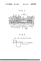
There has conventionally been proposed a solid state imager device as shown in FIG. 1.
In FIG. 1, there is formed on the surface of a P-type silicon substrate 1 a charge accumulating region 2 made of an N- -type region, an overflow control gate region 3 made of a P-type region adjacent to the charge accumulating region 2, and an overflow drain region 4 made of an N+ -type region adjacent to the overflow control region 3. Reference numeral 5 designates a channel stopper region, 6 a charge transfer region made of an N31 -type region, 7 a transfer electrode made of polycrystalline silicon, and 8 and 9 SiO2 layers, respectively.
The above-mentioned solid state imager device is generally referred to as a lateral overflow-structured solid state imager device. When excessive signal charges are produced due to the irradiation of intense light, they are drawn out from the charge accumulating region 2 through the overflow control gate region 3 to the overflow drain region 4 and consequently absorbed in the overflow drain region 4. Therefore, the imager device having such structure can satisfactorily remove brooming.
However, since solid state imager device of the lateral overflow structure is such that the overflow control gate region 3 and the overflow drain region 4 are juxtaposed adjacent to the charge accumulating region 2 on the surface of the P-type silicon substrate 1, a dimension or area per one pixel is increased by these regions, so that high integration of the imager device cannot be achieved.
There has also been proposed a so-called vertical overflow-structured solid state imager device as shown in FIG. 2. In such an imager device, a P-type diffusion region 11 is deposited on the surface of an N-type silicon substrate 10, and the charge accumulating region 2 made of an N31 -region is formed on the surface of the P-type diffusion region 11. When excessive signal charges are produced, they are drawn out through the P-type diffusion region 11 positioned directly below the charge accumulating region 2 to the N-type silicon substrate 10 and absorbed in the N-type silicon substrate 10. The imager device of such, vertical overflow structure can also satisfactorily remove brooming, similar to the aforementioned that of the lateral overflow structure.
However, the solid state imager device of the vertical overflow structure has difficulty in forming the P-type diffusion region 11, so that its manufacturing process is quite restricted.
OBJECTS AND SUMMARY OF THE INVENTION
Accordingly, it is an object of the present invention to provide a solid state imager device which is capable of removing the above-mentioned inconvenience encountered in the prior art.
To achieve the above object, the present invention provides a solid state imager device having a charge accumulating region of a second conductivity type formed on the surface side of a semiconductor substrate of a first conductivity type, comprising:
(a) a charge accumulating section of the second conductivity type formed on the charge accumulating region, the second conductivity type region and the charge accumulating region, forming a charge accumulating section; and
(b) a first conductivity type region formed on the surface of and/or on the side of the second conductivity type region,
wherein if an excessive signal charge is produced in the charge accumulating section, the excessive signal charge is absorbed in the first conductivity type region.
These and other objects, feature and advantages of the present invention will become apparent from the following detailed description of the preferred embodiment taken in conjunction with the accompanying drawings, throughout which like reference numerals designate like elements and parts.
BRIEF DESCRIPTION OF THE DRAWINGS
FIG. 1 is a cross-sectional view showing a main portion of an example of a previously proposed solid state imager device;
FIG. 2 is a cross-sectional view showing a main portion of another example of a previously proposed solid state imager device;
FIG. 3 is a cross-sectional view showing a main portion of an embodiment of a solid state imager device according to the present invention;
FIG. 4 is a top plan view taken along a line IV--IV' of FIG. 3;
FIG. 5 is a graph showing the potential level of the respective parts of the solid state imager device shown in FIG. 3;
FIGS. 6, 8, 10, 12, 14, 16, 18, 20 and 22 are partial plan views respectively showing a manufacturing process of the solid state imager device shown in FIG. 3;
FIG. 7 is a cross-sectional view taken along a line VII--VII' of FIG. 6;
FIG. 9 is a cross-sectional view taken along a line IX--IX' of FIG. 8;
FIG. 11 is a cross-sectional view taken along a line XI--XI' of FIG. 10;
FIG. 13 is a cross-sectional view taken along a line XIII--XIII' of FIG. 12;
FIG. 15 is a cross-sectional view taken along a line XV--XV' of FIG. 14;
FIG. 17 is a cross-sectional view taken along a line XVII--XVII' of FIG. 16;
FIG. 19 is a cross-sectional view taken along a line XIX--XIX' of FIG. 18;
FIG. 21 is a cross-sectional view taken along a line XXI--XXI' of FIG. 20; and
FIG. 23 is a cross-sectional view taken along a line XXIII--XXIII' of FIG. 22;
DESCRIPTION OF THE PREFERRED EMBODIMENT
An embodiment of a solid state imager device according to the present invention will hereinafter be described with reference to FIGS. 3 to 23. The description is given to a case where the present invention is applied to a solid state imager device which employs the interline transfer system. The parts in FIGS. 3-23 corresponding to those in FIGS. 1 and 2 are designated by the same reference numerals.
First, the structure of the present embodiment is explained with reference to FIGS. 3 to 5.
On the surface of a P-type silicon substrate 1, there are formed an N- -type region 2 serving as a charge accumulating region, an N- -type region 6 sering as a charge transfer region and a P+ -type region 5 serving as a channel stopper region, respectively. In this case, there are provided, for example, horizontally 492 and vertically 800 of the N--type regions 2 in the form of a matrix.
Transfer electrodes 7A and 7B are formed on the charge transfer region 6 through an SiO2 layer 16. These transfer electrodes 7A and 7B and the charge transfer electrode 6 form a vertical register section 17 which is operative to transfer signal charges read out of the charge accumulating region 2 to a horizontal register section (not shown) by a so-called four phase drive. The transfer electrodes 7A and 7B are respectively made of polycrystalline silicon doped with impurities to reduce their resistances. Further, the transfer electrodes 7A and 7B extend over a read-out gate region 15 on the P-type silicon substrate 1 so as to be used also as the read-out gate region 15. The SiO2 layer 16 is provided, on the charge accumulating region 2, with a rectangular opening 18 which is smaller than the charge accumulating region 2 in area. An output section and the horizonatal register section are constructed in a known manner, though not shown in FIGS. 3 and 4.
Further, there are deposited an SiO2 layer 19 over the transfer electrodes 7A and 7B and also an SiO2 layer 20 over the SiO2 layers 19 and 16. An opening 21 is provided through the SiO2 layer 20 which is coincident with the opening 18 through the SiO2 layer 16. A light shielding layer 22 is provided on the upper surface of the SiO2 layer 20 to protect the vertical register section 17 from irradiation to thereby prevent a so-called smear.
An N--type region 12 extending over the light shielding layer 22 on the SiO2 layer 20 through the opening 18 and the opening 21 of the SiO2 layer 16 and the SiO2 layer 20 is deposited by the epitaxial growth techniques. The N31 - type regions 12 and 2 form a change accumulating section 13. The dimension or area of the upper surface of the N- -type region 12 is made a bit larger than the dimension or area of the N- -type region 2.
A P+ -type region 14 is provided on the side surface of the N- -type region 12 to form a PN junction with the N- -type region 12. The P+ -type region 14 is provided on the surface thereof with an SiO2 layer 23 serving as a protective layer through which formed is an opening 24 which is positioned on the P+ -type region 14. An alminum wiring layer 25 which is connected in ohmic with the P+ -type region 14 through the opening 24 is deposited on the SiO2 layer 23 such that it does not shield a light receiving face 26.
In this embodiment, the channel stopper region 5 is made, for example, at zero volt, and the read out gate region 15, for example, at three volts. The P+ -type region 14 is supplied, for example, with direct-current four volts through the alminum wiring layer 25. The potential level in a region indicated by a two-dot chain line X in FIG. 3, that is, in the region over the channel stopper region 5, the charge transfer region 6, the read-out gate region 15, the N- -type region 2, the N- -type region 12 and the P+ -type region 14, is made as shown in FIG. 5. To be specific, the P+ -type region 14 has a deeper potential level than that of the read-out gate region 15.
Next, how the solid state imager device of the present embodiment is manufactured will be explained with reference to FIGS. 6 to 23. However, the explanation is limited to only the parts shown in FIGS. 3 and 4.
Referring first to FIGS. 6 and 7, the P-type silicon substrate 1 is prepared and then selectively ion-implanted with P-type impurities to form the P+ -type region 5 which is to serve as a channel stopper region.
Next, as shown in FIGS. 8 and 9, the P-type silicon substrate 1 is selectively ion-implanted with N-type impurities to form the N- -type region 2 serving as the charge accumulating region and the N- -type region 6 serving as the charge transfer region.
Next, as shown in FIGS. 10 and 11, the SiO2 layer 16 is deposited all over the upper surface of the device shown in FIG. 9, for example, by chemical vapor deposition (CVD) techniques, and then the transfer electrode 7A made of polycrystalline silicon is formed on the SiO2 layer 16.
Next, after forming an inter-layer insulating layer on the transfer electrodes 7A, the transfer electrode 7B which serves also as the read-out gate is formed with polycrystalline silicon, as shown in FIGS. 12 and 13.
Next, as shown in FIGS. 14 and 15, the transfer electrode 7B is covered with the SiO2 layer 19 formed by the thermal oxidation. Then, the SiO2 layer 20 is deposited all over the surface thereof by the CVD techniques.
Next, as shown in FIGS. 16 and 17, the rectangular-shaped openings 18 and 21 smaller than the charge accumulating region 2 in area are provided through the SiO2 layers 16 and 20 on the charge accumulating region 2. Then, the light shielding layer 22 made of light reflective or light absorbing material is deposited on the Si02 layer 20.
Next, as shown in FIGS. 18 and 19, a silicon layer 27 is deposited on all the surface of the device shown in FIG. 17, with the surface of the N- -type region 2 exposed by the openings 18 and 21 used as a seeding crystal.
Next, as shown in FIGS. 20 and 21, the silicon layer 27 is selectively ion-implanted with N-type impurities and P-type impurities to form the N- -type region 12, whose center portion is a silicon layer 27A in the openings 18 and 21 and whose upper plane portion is a bit wider than that of the N- -type region 2, and the P+ -type region 14 occupies portions other than the N- -type region 12.
Next, as shown in FIGS. 22 and 23, the SiO2 layer 23 is deposited all over the surface of the N- -type region 12 and the P+ -type region 14 by the CVD techniques. Then, the opening 24 is formed at a predetermined position of the SiO2 layer 23 on the P+ -type region 14.
Next, the alminum wiring layer 25 which is ohmically connected with the P+ -type region 14 through the opening 24 is deposited on the SiO2 layer 23 such that it does not shield the light receiving face 26. Finally, the alminum wiring layer 25 is treated to be applied, for example, with direct-current four volts, whereby the solid state imager device of the present embodiment shown in FIG. 3 is completed.
Signal charges produced when the light receiving face 26 is irradiated with light are accumulated in the charge accumulating section 13 formed of the N- - type regions 2 and 12 and ordinally read out to the vertical register section 17 through the read-out gate region 15.
On the other hand, if signal charges exceeding the capacity of the charge accumulating section 13 are produced by intense light irradiating the light receiving face 26, since the potential level of the P+ -type region 14 is made lower than that of the gateregion 15, the excessive signal charges never flow into other charge accumulating regions but are drawn out to the P+ -type region 14. In this case, the P+ -type region 14 and the N- -type region 12 form the PN junction and holes exist in the P+ -type region 14 as the majority carrier, so that the signal charges (electrons) drawn to the P+ -type region 14 are recombined with the holes in the P+ -type region 14. Thus, brooming can be satisfactorily removed.
According to the present embodiment, it is not necessary to provide the region, to which excessive signal charges are discharged, on the surface of the semiconductor substrate adjacent to the charge accumulating region as the lateral overflow-structured solid state imager device, so that a dimension or area per one pixel can be reduced, whereby high integration can be achieved.
Also, in this invention it is not necessary to form on the N-type silicon substrate the P-type diffusion region which has difficulty in forming conditions, as the vertical overflow-structured solid state imager device, so that the manufacture thereof becomes more easily.
The above-described embodiment is the case where the present invention is applied to an interline transfer solid state imager device. Apart from that, the present invention can be also applied to a MOS-type solid state imager device, wherein the same effects as described above can be achieved.
The above description is given on a single preferred embodiment of the invention but it will be apparent that many modifications and variations could be effected by one skilled in the art without departing from the spirits or scope of the novel concepts of the invention so that the scope of the invention shou1d be determined by the appended claim only.

Claims (1)

I claim as my invention:
1. A solid state imager device having a charge accumulating region of a second conductivity type formed on the surface side of a semiconductor substrate of a first conductivity type, comprising:
(a) a charge accumulating section of the second conductivity type formed on said charge accumulating region, said second conductivity type region and said charge accumulating region, forming a charge accumulating section; and
(b) a first conductivity type region formed on the surface of and/or on the side of said second conductivity type region,
wherein if an excessive signal charge is produced in said charge accumulating section, said excessive signal charge is absorbed in said first conductivity type region.
US07/143,651 1987-01-16 1988-01-13 Solid state imager device Expired - Fee Related US4851887A (en)

Applications Claiming Priority (2)

Application Number Priority Date Filing Date Title
JP62007655A JPS63177460A (en) 1987-01-16 1987-01-16 Solid-state image device
JP62-7655 1987-01-16

Publications (1)

Publication Number Publication Date
US4851887A true US4851887A (en) 1989-07-25

Family

ID=11671832

Family Applications (1)

Application Number Title Priority Date Filing Date
US07/143,651 Expired - Fee Related US4851887A (en) 1987-01-16 1988-01-13 Solid state imager device

Country Status (4)

Country Link
US (1) US4851887A (en)
EP (1) EP0275180A3 (en)
JP (1) JPS63177460A (en)
KR (1) KR880009450A (en)

Cited By (10)

* Cited by examiner, † Cited by third party
Publication number Priority date Publication date Assignee Title
US4994876A (en) * 1988-08-31 1991-02-19 Mitsubishi Denki Kabushiki Kaisha Light detecting element and light detecting array
US5005062A (en) * 1988-08-10 1991-04-02 U.S. Philips Corporation Image sensor device of the frame transfer type
US5051798A (en) * 1989-04-07 1991-09-24 Mitsubishi Denki Kabushiki Kaisha Solid state image sensing device having an overflow drain structure
US5055930A (en) * 1989-09-13 1991-10-08 Olympus Optical Co., Ltd. Image sensing and recording device having a multilayer analog memory stacked on an image sensing array
WO1992001312A1 (en) * 1990-07-12 1992-01-23 Eastman Kodak Company Antiblooming structure for solid-state image sensor
US5170236A (en) * 1991-05-01 1992-12-08 Kabushiki Kaisha Toshiba Layer-built solid state image sensing device
US5235198A (en) * 1989-11-29 1993-08-10 Eastman Kodak Company Non-interlaced interline transfer CCD image sensing device with simplified electrode structure for each pixel
US5313081A (en) * 1990-07-19 1994-05-17 Kabushiki Kaisha Toshiba Solid-state imaging device with transport channels between photosensitive elements
US5343061A (en) * 1992-05-27 1994-08-30 Kabushiki Kaisha Toshiba Solid-state imaging device suppressing dark-current noise
US20030162273A1 (en) * 2002-02-04 2003-08-28 Anastasios Melis Modulation of sulfate permease for photosynthetic hydrogen production

Families Citing this family (1)

* Cited by examiner, † Cited by third party
Publication number Priority date Publication date Assignee Title
JP6386777B2 (en) * 2014-05-08 2018-09-05 浜松ホトニクス株式会社 Distance image sensor

Citations (4)

* Cited by examiner, † Cited by third party
Publication number Priority date Publication date Assignee Title
US4369458A (en) * 1980-07-01 1983-01-18 Westinghouse Electric Corp. Self-aligned, flip-chip focal plane array configuration
US4737833A (en) * 1985-02-22 1988-04-12 Fuji Photo Film Co., Ltd. Solid-state color image pickup device with accumulated-layer structure
US4740824A (en) * 1985-07-18 1988-04-26 Kabushiki Kaisha Toshiba Solid-state image sensor
US4748486A (en) * 1984-08-27 1988-05-31 Sharp Kabushiki Kaisha Solid-state image sensor

Family Cites Families (3)

* Cited by examiner, † Cited by third party
Publication number Priority date Publication date Assignee Title
JPS5812481A (en) * 1981-07-15 1983-01-24 Toshiba Corp Solidstate image pickup element
JPS6029095A (en) * 1983-07-28 1985-02-14 Matsushita Electric Ind Co Ltd Image pickup device and its manufacturing method
JPS61187267A (en) * 1985-02-14 1986-08-20 Matsushita Electric Ind Co Ltd Solid-state image pickup device

Patent Citations (4)

* Cited by examiner, † Cited by third party
Publication number Priority date Publication date Assignee Title
US4369458A (en) * 1980-07-01 1983-01-18 Westinghouse Electric Corp. Self-aligned, flip-chip focal plane array configuration
US4748486A (en) * 1984-08-27 1988-05-31 Sharp Kabushiki Kaisha Solid-state image sensor
US4737833A (en) * 1985-02-22 1988-04-12 Fuji Photo Film Co., Ltd. Solid-state color image pickup device with accumulated-layer structure
US4740824A (en) * 1985-07-18 1988-04-26 Kabushiki Kaisha Toshiba Solid-state image sensor

Cited By (11)

* Cited by examiner, † Cited by third party
Publication number Priority date Publication date Assignee Title
US5005062A (en) * 1988-08-10 1991-04-02 U.S. Philips Corporation Image sensor device of the frame transfer type
US4994876A (en) * 1988-08-31 1991-02-19 Mitsubishi Denki Kabushiki Kaisha Light detecting element and light detecting array
US5051798A (en) * 1989-04-07 1991-09-24 Mitsubishi Denki Kabushiki Kaisha Solid state image sensing device having an overflow drain structure
US5114865A (en) * 1989-04-07 1992-05-19 Mitsubishi Denki Kabushiki Kaisha Method of manufacturing a solid-state image sensing device having an overflow drain structure
US5055930A (en) * 1989-09-13 1991-10-08 Olympus Optical Co., Ltd. Image sensing and recording device having a multilayer analog memory stacked on an image sensing array
US5235198A (en) * 1989-11-29 1993-08-10 Eastman Kodak Company Non-interlaced interline transfer CCD image sensing device with simplified electrode structure for each pixel
WO1992001312A1 (en) * 1990-07-12 1992-01-23 Eastman Kodak Company Antiblooming structure for solid-state image sensor
US5313081A (en) * 1990-07-19 1994-05-17 Kabushiki Kaisha Toshiba Solid-state imaging device with transport channels between photosensitive elements
US5170236A (en) * 1991-05-01 1992-12-08 Kabushiki Kaisha Toshiba Layer-built solid state image sensing device
US5343061A (en) * 1992-05-27 1994-08-30 Kabushiki Kaisha Toshiba Solid-state imaging device suppressing dark-current noise
US20030162273A1 (en) * 2002-02-04 2003-08-28 Anastasios Melis Modulation of sulfate permease for photosynthetic hydrogen production

Also Published As

Publication number Publication date
EP0275180A3 (en) 1989-06-28
KR880009450A (en) 1988-09-15
JPS63177460A (en) 1988-07-21
EP0275180A2 (en) 1988-07-20

Similar Documents

Publication Publication Date Title
US4373167A (en) Solid state image sensor with overflow protection and high resolution
US5051797A (en) Charge-coupled device (CCD) imager and method of operation
US4168444A (en) Imaging devices
US4851887A (en) Solid state imager device
US5306931A (en) CCD image sensor with improved antiblooming characteristics
FR2641417A1 (en) MOS TYPE SEMICONDUCTOR DEVICE
US4686555A (en) Solid state image sensor
US4975777A (en) Charge-coupled imager with dual gate anti-blooming structure
GB1394520A (en) Charge coupled device area imaging array
JPH07107928B2 (en) Solid-state imaging device
JPS6065565A (en) Solid-state image sensor
US4974043A (en) Solid-state image sensor
US5196692A (en) Photoelectric transducer switchable to a high-resolution or high-sensitivity mode
US6403994B1 (en) Solid-state imaging device and method of fabricating the same
CA1106477A (en) Overflow channel for charge transfer imaging devices
GB2054961A (en) Excess Charge Removal in Charge Transfer Devices
JPS58125970A (en) Solid-state image pickup device
JPS6043031B2 (en) infrared detection device
JPS6318387B2 (en)
JPH0449787B2 (en)
JP2901328B2 (en) Solid-state imaging device
JPS6320384B2 (en)
JP2805848B2 (en) Solid-state imaging device
JPS6320385B2 (en)
KR970004493B1 (en) A method for manufacture and structure of semiconductor device

Legal Events

Date Code Title Description
AS Assignment

Owner name: SONY CORPORATION, 7-35 KITASHINAGAWA-6, SHINAGAWA-

Free format text: ASSIGNMENT OF ASSIGNORS INTEREST.;ASSIGNOR:HAGIWARA, YOSHIAKI;REEL/FRAME:004822/0163

Effective date: 19871228

Owner name: SONY CORPORATION, A CORP. OF JAPAN,JAPAN

Free format text: ASSIGNMENT OF ASSIGNORS INTEREST;ASSIGNOR:HAGIWARA, YOSHIAKI;REEL/FRAME:004822/0163

Effective date: 19871228

FEPP Fee payment procedure

Free format text: PAYOR NUMBER ASSIGNED (ORIGINAL EVENT CODE: ASPN); ENTITY STATUS OF PATENT OWNER: LARGE ENTITY

FPAY Fee payment

Year of fee payment: 4

REMI Maintenance fee reminder mailed
LAPS Lapse for failure to pay maintenance fees
FP Lapsed due to failure to pay maintenance fee

Effective date: 19970730

STCH Information on status: patent discontinuation

Free format text: PATENT EXPIRED DUE TO NONPAYMENT OF MAINTENANCE FEES UNDER 37 CFR 1.362