US4757610A - Surface mount network and method of making - Google Patents
Surface mount network and method of making Download PDFInfo
- Publication number
- US4757610A US4757610A US07/110,323 US11032387A US4757610A US 4757610 A US4757610 A US 4757610A US 11032387 A US11032387 A US 11032387A US 4757610 A US4757610 A US 4757610A
- Authority
- US
- United States
- Prior art keywords
- end caps
- network
- grooves
- set forth
- parallel
- Prior art date
- Legal status (The legal status is an assumption and is not a legal conclusion. Google has not performed a legal analysis and makes no representation as to the accuracy of the status listed.)
- Expired - Fee Related
Links
Images

Classifications
-
- H—ELECTRICITY
- H05—ELECTRIC TECHNIQUES NOT OTHERWISE PROVIDED FOR
- H05K—PRINTED CIRCUITS; CASINGS OR CONSTRUCTIONAL DETAILS OF ELECTRIC APPARATUS; MANUFACTURE OF ASSEMBLAGES OF ELECTRICAL COMPONENTS
- H05K5/00—Casings, cabinets or drawers for electric apparatus
- H05K5/0091—Housing specially adapted for small components
-
- H—ELECTRICITY
- H01—ELECTRIC ELEMENTS
- H01C—RESISTORS
- H01C13/00—Resistors not provided for elsewhere
- H01C13/02—Structural combinations of resistors
-
- H—ELECTRICITY
- H01—ELECTRIC ELEMENTS
- H01C—RESISTORS
- H01C17/00—Apparatus or processes specially adapted for manufacturing resistors
- H01C17/006—Apparatus or processes specially adapted for manufacturing resistors adapted for manufacturing resistor chips
-
- H—ELECTRICITY
- H05—ELECTRIC TECHNIQUES NOT OTHERWISE PROVIDED FOR
- H05K—PRINTED CIRCUITS; CASINGS OR CONSTRUCTIONAL DETAILS OF ELECTRIC APPARATUS; MANUFACTURE OF ASSEMBLAGES OF ELECTRICAL COMPONENTS
- H05K3/00—Apparatus or processes for manufacturing printed circuits
- H05K3/30—Assembling printed circuits with electric components, e.g. with resistor
- H05K3/301—Assembling printed circuits with electric components, e.g. with resistor by means of a mounting structure
-
- Y—GENERAL TAGGING OF NEW TECHNOLOGICAL DEVELOPMENTS; GENERAL TAGGING OF CROSS-SECTIONAL TECHNOLOGIES SPANNING OVER SEVERAL SECTIONS OF THE IPC; TECHNICAL SUBJECTS COVERED BY FORMER USPC CROSS-REFERENCE ART COLLECTIONS [XRACs] AND DIGESTS
- Y10—TECHNICAL SUBJECTS COVERED BY FORMER USPC
- Y10T—TECHNICAL SUBJECTS COVERED BY FORMER US CLASSIFICATION
- Y10T29/00—Metal working
- Y10T29/49—Method of mechanical manufacture
- Y10T29/49002—Electrical device making
- Y10T29/49082—Resistor making
- Y10T29/49087—Resistor making with envelope or housing
-
- Y—GENERAL TAGGING OF NEW TECHNOLOGICAL DEVELOPMENTS; GENERAL TAGGING OF CROSS-SECTIONAL TECHNOLOGIES SPANNING OVER SEVERAL SECTIONS OF THE IPC; TECHNICAL SUBJECTS COVERED BY FORMER USPC CROSS-REFERENCE ART COLLECTIONS [XRACs] AND DIGESTS
- Y10—TECHNICAL SUBJECTS COVERED BY FORMER USPC
- Y10T—TECHNICAL SUBJECTS COVERED BY FORMER US CLASSIFICATION
- Y10T29/00—Metal working
- Y10T29/49—Method of mechanical manufacture
- Y10T29/49002—Electrical device making
- Y10T29/49117—Conductor or circuit manufacturing
- Y10T29/49124—On flat or curved insulated base, e.g., printed circuit, etc.
- Y10T29/4913—Assembling to base an electrical component, e.g., capacitor, etc.
Definitions
- the present invention relates generally to an assembly of electrical components on a common support, hereinafter called a network, said network capable of being mounted on the surface of a printed circuit board.
- the present invention also relates to a method of making said network.
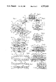
- FIG. 1 illustrates one method of assembling varying components to make one form of the surface mount network.
- FIG. 2 is an exploded partial sectional view of the surface mount network shown in FIG. 1 and also illustrating a portion of a printed circuit board.
- FIG. 3 is a section taken generally along the line 3--3 in FIG. 1 of a completed first form of surface mount network, the network being inverted and shown mounted on a printed circuit board.
- FIG. 4 is a section taken generally along the line 4--4 in FIG. 3.
- FIG. 5 shows a second form of a surface mount network, parts being broken out for purposes of clarity.
- FIG. 6 is a section taken generally along the line 6--6 in FIG. 5, this section also being inverted and shown mounted on a printed circuit board.
- FIG. 6A is a view similar to FIG. 6 showing an alternate construction of the second form of the surface mount network of FIGS. 5 and 6.
- FIGS. 7, 8 and 9 are side, top and end views, respectively, of a third form of the surface mount network of this invention.
- FIG. 10 is a schematic illustration showing how individual electrical components can be molded into a network.
- FIGS. 1-4 A first form of resistor network is illustrated in FIGS. 1-4, this form being a single in-line resistor network.
- the network indicated generally at 10, includes a column or array of a plurality of identically dimensioned resistors, indicated generally at 12, which are disposed within a rigid common dielectric support 16.
- Each of the resistors consists of a cylindrical resistance body 18 consisting of an aluminous slug having a spirally cut nichrome layer and a pair of electrically conductive end caps 20, the cylindrical walls 22 of the end caps being press fit onto opposite ends of the aluminous slug.
- the rigid common support 16 which is illustrated in FIGS. 1-4 is a rigid bar stock 16a of dielectric material which may be initially of a generally rectangular cross section having parallel sides 24 and 26, and parallel surfaces 28 and 29 at right angles to the surface 24 and 26. Grooves 14 are formed in the bar stock in such a manner that they are parallel to each other and at right angles to parallel sides 24, 26. Thus, the grooves can be cut into surface 28 of the bar stock, or alternatively the support 16a can be molded to its final form.
- the distance between the two parallel sides 24, 26 of the support 16 is equal to or preferably slightly less than the distance of the elongated component body 18 between end caps 20.
- the grooves 14 are identically dimensioned and each groove has a cylindrical bottom 30, all bottoms 30 lying in a common plane parallel to the surface 28.
- the depth of the grooves 14 from the surface 28 does not exceed the diameter of the cylindrical component body plus the thickness of a cylindrical wall 22 so that after the components 12 are fully mounted within the grooves an exposed exterior surface portion 32 of the end caps will project above the surface 28.
- the exposed surface portion 32 of each end cap will lie in a common plane on the periphery of the network.
- the support further includes dielectric material 16b which is placed over the surface portion of the component bodies which is initially exposed after the component body has been placed within the grooves 14 of the bar stock 16.
- the thickness of the insulating material is such that it does not project beyond the common plane defined by the exposed portions 32. As the plane of the exposed portions 32 are on the periphery of the network, these portions can be mounted upon the conductive traces 36 of a printed circuit board 38.
- an adhesive in the groove to rigidly secure the resistor in place within the groove, such an adhesive, for example, being a one component epoxy which glues when heated.
- the insulation which is placed over the resistors after they have been placed in the grooves can be a liquid epoxy or any other suitable material. In any event, it is essential that the exposed portions 32 of the end caps which are to contact the conductive trace 36 on the printed circuit board all lie in the same plane and thus dimensioning is very critical.
- the metalized aluminous slug be completely sealed from moisture from end cap to end cap. This can be accomplished by the assembly procedure set forth above. However, in some situations, this will be done as a separate step. Thus, after the end caps have been applied to the nichrome coated aluminous slug, the slug can be coated with a suitable moisture proofing coating from end cap to end cap.
- FIGS. 5-9 Dual in-line networks are illustrated in FIGS. 5-9.
- the forms illustrated in FIGS. 5, 6 and 6A will be called parallel dual in-line networks in that the resistors will be mounted parallel to the surface of the printed circuit board.
- FIGS. 7-9 will be referred to as perpendicular dual in-line networks.
- a rigid common support 40 of dielectric material which again can initially be of rectangular cross section, is initially provided with a channel 42, the channel being parallel to parallel sides 44, 46.
- the channel will also be of rectangular cross section and it too will have parallel adjacent sides 48, 50.
- the distance between the surfaces 44 and 48 and also between the surfaces 50 and 46 is less than, but preferably nearly equal to, the length of the component body between the end caps of the resistors which are to be placed in the grooves.
- the distance between the surfaces 48 and 50 is at least equal to the length of a pair of adjacent end caps and preferably is sufficiently wide so that a common bus 54 may be electrically connected between adjacent end caps. As can be seen from FIG. 6, in most applications only the outermost end caps will be secured to the conductive traces.
- a parallel dual in-line resistor network can also be constructed by mounting two single in-line resistor networks on a common support 56 by welding or by utilizing a suitable adhesive, the common support 56 being substantially rigid.
- the common bus 54a which extends between the end caps, may be of a ribbon form rather than the wire form shown in FIG. 6 to facilitate the assembliy of the parts.
- resistors When using a single in-line resistor network of the design of FIG. 1, resistors will be selected for insertion into the grooves, which resistors may correspond to the required values of a particular circuit, or which alternatively may be a range of resistors.
- one of the selected resistors 12a may be a zero ohm resistor.
- a zero ohm resistor has a cylindrical copper core disposed between its end caps.
- the resistors may be selected having differing values and by properly connecting the end caps to the conductive traces on the printed circuit board, a wide variety of values may be secured from a single network package.
- FIGS. 7-9 A perpendicular dual in-line resistor network is illustrated in FIGS. 7-9.
- the two in-line resistors can be identically dimensioned, as illustrated, or they may have varying spacings between the individual resistors.
- a common bus 58 is placed between adjacent end caps 20. Again one of the various components may be a zero ohm resistor.
- FIGS. 7-9 utilizes two separate single inline resistor networks which are adhered to each other, an alternate design may be to employ a common rigid support which is then provided with two rows of identically dimensioned grooves on opposite sides, the electrical components then being placed within the various grooves.
- Insulation is then placed over the resistors after they have been placed in the grooves in a manner similar to that illustrated in FIG. 1.
- the design is such that the planar surface 62 of the end caps not connected to bus 58 all lie in a common plane on the periphery of the network.
- an indicator may be provided on the common support to indicate one of the electrical components to facilitate assembly onto a printed circuit board.
- an indicator 60 may be provided. While an indicator has only been shown in connections with the design of FIGS. 7-9, it should be obvious that an indicator may be provided in any network design of this invention.
- the support 16 can be an integral piece of rigid dielectric material molded about the resistors 12. More specifically, with reference to FIG. 10, individual resistors 12 can be suitably positioned in a mold cavity 64 in the lower half of a mold. When the mold cavity is closed by bringing the top half 68 and the bottom half 66 together, the end caps will be engaged by the mold. It is then only necessary to introduce the molding material through feed 70, feeder base 72, runner 74, and gate 76, the air within the mold being bled to atmosphere through bleed 78.
- the lower mold half 66 is provided with suitable alignment pins 80 which are received within suitable bushings (not shown) in the upper mold half 68. If this were the case, opposed end caps 20 would be supported by a suitable mold in a columnar array, the support then being molded about the cylindrical resistance bodies to the final form. If desired, the resistance bodies can be coated prior to molding with a moisture resistant material. Hoewver, in most molding processes, such as transfer molding, compression molding, and injection molding, if there is suitable adhesion between the molding material and the cylindrical resistance bodies, it will not be necessary to provide any additional moisture resistance material.
- the final molded product will not have the end caps covered with molding material, at least upon the surface which is to be in contact with the conductive traces 36 on the printed circuit board, and if there is any flashing material in this area, it can readily be removed. Any flashing which is present to the sides of the support 16 will not have to be removed unless it is excessive. While only one form of a suitable mold is illustrated in the drawings, the design of various other molds should be obvious to one having ordinary skill in the molding art from the above description.
- a parallel dual in-line resistor network may also be formed by molding wherein opposed end caps of aligned resistors are firmly held by a mold to maintain adjacent pairs in relatively coaxially alignment, the common bus either being secured between adjacent end caps prior to molding or by inserting a mold resist material between end caps prior to molding, the resist material subsequently being removed and the common bus then being secured between adjacent caps.
- the perpendicular dual in-line resistor network can also be formed by a molding process wherein all of the end caps shown at the bottom in FIG. 7 are placed within suitable apertures in the bottom of a mold, and the molding material being molded up to the top surface 26 shown in FIG. 7. The bus 58 can then be inserted.
- the various networks of this invention can be assembled onto the surface of a printed circuit board by conventional methods.
- the completed components can be picked and placed onto the conductive strips of the board, which would initially have a solder paste on the board where the desired connections are to be made, and which could also have an adhesive to hold the network on the board.
- the board is then heated to melt the solder paste and to set an adhesive if an adhesive is used. After these steps are performed, the printed circuit board is then washed.
Abstract
Description
Claims (24)
Priority Applications (1)
| Application Number | Priority Date | Filing Date | Title |
|---|---|---|---|
| US07/110,323 US4757610A (en) | 1986-02-21 | 1987-10-20 | Surface mount network and method of making |
Applications Claiming Priority (2)
| Application Number | Priority Date | Filing Date | Title |
|---|---|---|---|
| US83158286A | 1986-02-21 | 1986-02-21 | |
| US07/110,323 US4757610A (en) | 1986-02-21 | 1987-10-20 | Surface mount network and method of making |
Related Parent Applications (1)
| Application Number | Title | Priority Date | Filing Date |
|---|---|---|---|
| US83158286A Continuation-In-Part | 1986-02-21 | 1986-02-21 |
Publications (1)
| Publication Number | Publication Date |
|---|---|
| US4757610A true US4757610A (en) | 1988-07-19 |
Family
ID=26807914
Family Applications (1)
| Application Number | Title | Priority Date | Filing Date |
|---|---|---|---|
| US07/110,323 Expired - Fee Related US4757610A (en) | 1986-02-21 | 1987-10-20 | Surface mount network and method of making |
Country Status (1)
| Country | Link |
|---|---|
| US (1) | US4757610A (en) |
Cited By (7)
| Publication number | Priority date | Publication date | Assignee | Title |
|---|---|---|---|---|
| US4829406A (en) * | 1988-03-04 | 1989-05-09 | General Instrument Corp. | Square body leadless electrical device |
| US6097277A (en) * | 1998-11-05 | 2000-08-01 | Cts | Resistor network with solder sphere connector |
| US20050024839A1 (en) * | 2003-07-31 | 2005-02-03 | Bloom Terry R. | Ball grid array package |
| US20050035450A1 (en) * | 2003-08-13 | 2005-02-17 | David Poole | Ball grid array package having testing capability after mounting |
| US20050052854A1 (en) * | 2003-09-09 | 2005-03-10 | Hewlett-Packard Company | Configurable circuit board and fabrication method |
| USRE39453E1 (en) | 1999-10-28 | 2007-01-02 | Coilcraft, Incorporated | Low profile inductive component |
| US9978486B2 (en) * | 2016-01-19 | 2018-05-22 | Fluke Corporation | Load resistor supports |
Citations (27)
| Publication number | Priority date | Publication date | Assignee | Title |
|---|---|---|---|---|
| US1932650A (en) * | 1930-12-18 | 1933-10-31 | Int Resistance Co | Resistance |
| US2441960A (en) * | 1943-02-02 | 1948-05-25 | Eisler Paul | Manufacture of electric circuit components |
| US2552626A (en) * | 1948-02-17 | 1951-05-15 | Bell Telephone Labor Inc | Silicon-germanium resistor and method of making it |
| US2777039A (en) * | 1954-06-29 | 1957-01-08 | Standard Coil Prod Co Inc | Resistor elements adapted for use in connection with printed circuits |
| US2903666A (en) * | 1955-08-23 | 1959-09-08 | Speer Carbon Company | Resistors with integral molded metal terminals |
| US3272909A (en) * | 1964-11-04 | 1966-09-13 | Avco Corp | Printed circuit package with indicia |
| US3302272A (en) * | 1963-12-26 | 1967-02-07 | Air Reduction | Forming a resistor with thin, compressed, contact portions |
| US3345598A (en) * | 1964-04-25 | 1967-10-03 | Telefunken Patent | Circuit element |
| US3346775A (en) * | 1965-06-19 | 1967-10-10 | Interlego Ag | Components for making structures comprising electrical circuits |
| US3410949A (en) * | 1967-10-16 | 1968-11-12 | Tischler Morris | Plastic embedded color-coded printed circuit |
| US3444436A (en) * | 1967-04-26 | 1969-05-13 | Erie Technological Prod Inc | Mounted capacitor with spaced terminal feet |
| US3456159A (en) * | 1963-08-08 | 1969-07-15 | Ibm | Connections for microminiature functional components |
| US3550228A (en) * | 1967-11-29 | 1970-12-29 | Jean Claude Asscher | Method of assembling leads to an electrical component and potting same |
| US3697818A (en) * | 1970-01-23 | 1972-10-10 | Sovcor Electronique | Encapsulated cordwood type electronic or electrical component assembly |
| US3930306A (en) * | 1974-04-24 | 1976-01-06 | General Instrument Corporation | Process for attaching a lead member to a semiconductor device |
| US3967296A (en) * | 1972-10-12 | 1976-06-29 | General Electric Company | Semiconductor devices |
| US4208005A (en) * | 1978-02-08 | 1980-06-17 | Hitachi, Ltd. | Method for mounting parts on circuit boards |
| US4267927A (en) * | 1979-10-22 | 1981-05-19 | English Jr Edgar | Article of manufacture comprising protective packaging for packageable objects of a fragile or perishable nature |
| US4312692A (en) * | 1979-03-09 | 1982-01-26 | Matsushita Electric Industrial Co., Ltd. | Method of mounting electronic components |
| US4337453A (en) * | 1979-03-08 | 1982-06-29 | Fuji Sangyo Kabushiki Kaisha | Fundamental electrical element array |
| US4339785A (en) * | 1979-04-26 | 1982-07-13 | Sony Corporation | Electronic circuit arrangement mounted on printed circuit board |
| US4349860A (en) * | 1979-04-13 | 1982-09-14 | Sony Corporation | Tantalum condenser |
| US4417298A (en) * | 1980-05-16 | 1983-11-22 | Koreaki Nakata | Chip type tantalum capacitor |
| US4449769A (en) * | 1979-04-11 | 1984-05-22 | Alps Electric Co., Ltd. | Substrate for mounting electric parts |
| US4489487A (en) * | 1981-02-10 | 1984-12-25 | Robert Bosch Gmbh | Electronic component and adhesive strip combination, and method of attachment of component to a substrate |
| US4542439A (en) * | 1984-06-27 | 1985-09-17 | At&T Technologies, Inc. | Surface mount component |
| US4564885A (en) * | 1984-09-10 | 1986-01-14 | General Instrument Corporation | Rectifier with slug construction and mold for fabricating same |
-
1987
- 1987-10-20 US US07/110,323 patent/US4757610A/en not_active Expired - Fee Related
Patent Citations (27)
| Publication number | Priority date | Publication date | Assignee | Title |
|---|---|---|---|---|
| US1932650A (en) * | 1930-12-18 | 1933-10-31 | Int Resistance Co | Resistance |
| US2441960A (en) * | 1943-02-02 | 1948-05-25 | Eisler Paul | Manufacture of electric circuit components |
| US2552626A (en) * | 1948-02-17 | 1951-05-15 | Bell Telephone Labor Inc | Silicon-germanium resistor and method of making it |
| US2777039A (en) * | 1954-06-29 | 1957-01-08 | Standard Coil Prod Co Inc | Resistor elements adapted for use in connection with printed circuits |
| US2903666A (en) * | 1955-08-23 | 1959-09-08 | Speer Carbon Company | Resistors with integral molded metal terminals |
| US3456159A (en) * | 1963-08-08 | 1969-07-15 | Ibm | Connections for microminiature functional components |
| US3302272A (en) * | 1963-12-26 | 1967-02-07 | Air Reduction | Forming a resistor with thin, compressed, contact portions |
| US3345598A (en) * | 1964-04-25 | 1967-10-03 | Telefunken Patent | Circuit element |
| US3272909A (en) * | 1964-11-04 | 1966-09-13 | Avco Corp | Printed circuit package with indicia |
| US3346775A (en) * | 1965-06-19 | 1967-10-10 | Interlego Ag | Components for making structures comprising electrical circuits |
| US3444436A (en) * | 1967-04-26 | 1969-05-13 | Erie Technological Prod Inc | Mounted capacitor with spaced terminal feet |
| US3410949A (en) * | 1967-10-16 | 1968-11-12 | Tischler Morris | Plastic embedded color-coded printed circuit |
| US3550228A (en) * | 1967-11-29 | 1970-12-29 | Jean Claude Asscher | Method of assembling leads to an electrical component and potting same |
| US3697818A (en) * | 1970-01-23 | 1972-10-10 | Sovcor Electronique | Encapsulated cordwood type electronic or electrical component assembly |
| US3967296A (en) * | 1972-10-12 | 1976-06-29 | General Electric Company | Semiconductor devices |
| US3930306A (en) * | 1974-04-24 | 1976-01-06 | General Instrument Corporation | Process for attaching a lead member to a semiconductor device |
| US4208005A (en) * | 1978-02-08 | 1980-06-17 | Hitachi, Ltd. | Method for mounting parts on circuit boards |
| US4337453A (en) * | 1979-03-08 | 1982-06-29 | Fuji Sangyo Kabushiki Kaisha | Fundamental electrical element array |
| US4312692A (en) * | 1979-03-09 | 1982-01-26 | Matsushita Electric Industrial Co., Ltd. | Method of mounting electronic components |
| US4449769A (en) * | 1979-04-11 | 1984-05-22 | Alps Electric Co., Ltd. | Substrate for mounting electric parts |
| US4349860A (en) * | 1979-04-13 | 1982-09-14 | Sony Corporation | Tantalum condenser |
| US4339785A (en) * | 1979-04-26 | 1982-07-13 | Sony Corporation | Electronic circuit arrangement mounted on printed circuit board |
| US4267927A (en) * | 1979-10-22 | 1981-05-19 | English Jr Edgar | Article of manufacture comprising protective packaging for packageable objects of a fragile or perishable nature |
| US4417298A (en) * | 1980-05-16 | 1983-11-22 | Koreaki Nakata | Chip type tantalum capacitor |
| US4489487A (en) * | 1981-02-10 | 1984-12-25 | Robert Bosch Gmbh | Electronic component and adhesive strip combination, and method of attachment of component to a substrate |
| US4542439A (en) * | 1984-06-27 | 1985-09-17 | At&T Technologies, Inc. | Surface mount component |
| US4564885A (en) * | 1984-09-10 | 1986-01-14 | General Instrument Corporation | Rectifier with slug construction and mold for fabricating same |
Cited By (12)
| Publication number | Priority date | Publication date | Assignee | Title |
|---|---|---|---|---|
| US4829406A (en) * | 1988-03-04 | 1989-05-09 | General Instrument Corp. | Square body leadless electrical device |
| US6097277A (en) * | 1998-11-05 | 2000-08-01 | Cts | Resistor network with solder sphere connector |
| USRE39453E1 (en) | 1999-10-28 | 2007-01-02 | Coilcraft, Incorporated | Low profile inductive component |
| US20050024839A1 (en) * | 2003-07-31 | 2005-02-03 | Bloom Terry R. | Ball grid array package |
| US7180186B2 (en) | 2003-07-31 | 2007-02-20 | Cts Corporation | Ball grid array package |
| US20070164433A1 (en) * | 2003-07-31 | 2007-07-19 | Bloom Terry R | Ball grid array package |
| US20050035450A1 (en) * | 2003-08-13 | 2005-02-17 | David Poole | Ball grid array package having testing capability after mounting |
| US6946733B2 (en) | 2003-08-13 | 2005-09-20 | Cts Corporation | Ball grid array package having testing capability after mounting |
| US20050052854A1 (en) * | 2003-09-09 | 2005-03-10 | Hewlett-Packard Company | Configurable circuit board and fabrication method |
| US7245501B2 (en) | 2003-09-09 | 2007-07-17 | Hewlett-Packard Development Company, L.P. | Configurable circuit board and fabrication method |
| US20070195510A1 (en) * | 2003-09-09 | 2007-08-23 | Kotson Michael A | Configurable circuit board and fabrication method |
| US9978486B2 (en) * | 2016-01-19 | 2018-05-22 | Fluke Corporation | Load resistor supports |
Similar Documents
| Publication | Publication Date | Title |
|---|---|---|
| US4547756A (en) | Multiple reed switch module | |
| US4193106A (en) | Monolithic ceramic capacitor with fuse link | |
| US4199209A (en) | Electrical interconnecting device | |
| US4494172A (en) | High-speed wire wrap board | |
| DE4013812A1 (en) | HERMETICALLY SEALED ELECTRICAL CONDUCTION WITH ELECTRIC FILTER ELEMENTS IN CHIPFORM | |
| JP3589494B2 (en) | Printed circuit board device with conductive mounting pins and its manufacturing method. | |
| EP0833550A2 (en) | Circuit board with strain relief for connecting cable, process for manufacturing and connecting the same as well as its use | |
| US3362005A (en) | Hinge type connector for circuit boards | |
| US5597326A (en) | Laminated miniature multi-conductor connector and method for manufacture | |
| JPH0412609B2 (en) | ||
| US4757610A (en) | Surface mount network and method of making | |
| GB8503454D0 (en) | Chip resistors | |
| EP0234838A2 (en) | Surface mount network and method of making | |
| US4406062A (en) | Method of forming a multichannel connector | |
| US4872092A (en) | Coupler terminal block | |
| US6587351B2 (en) | Surface mount standoff for printed circuit board assembly | |
| CA1080818A (en) | Electrical connection between two circuits cards | |
| JPS5812401Y2 (en) | Parallel resistor | |
| JP2580784Y2 (en) | Electronic circuit experiment equipment | |
| US4389697A (en) | Circuit assembly having a component with leads extending therefrom and a connector both supported on a planar substrate | |
| JPS6150365B2 (en) | ||
| JPH0126620Y2 (en) | ||
| US4777562A (en) | Wire wrap single in-line package | |
| US5244419A (en) | Electronic connector | |
| JPS6249614A (en) | Manufacture of electronic component |
Legal Events
| Date | Code | Title | Description |
|---|---|---|---|
| AS | Assignment |
Owner name: AMERICAN PRECISION INDUSTRIES, INC., 2777 WALDEN A Free format text: ASSIGNMENT OF ASSIGNORS INTEREST.;ASSIGNORS:MC ELHENY, DONALD C.;PONIVAS, DALE A.;REEL/FRAME:004820/0260 Effective date: 19871019 Owner name: AMERICAN PRECISION INDUSTRIES, INC., A CORP. OF NE Free format text: ASSIGNMENT OF ASSIGNORS INTEREST;ASSIGNORS:MC ELHENY, DONALD C.;PONIVAS, DALE A.;REEL/FRAME:004820/0260 Effective date: 19871019 |
|
| AS | Assignment |
Owner name: AMERICAN PRECISION INDUSTRIES INC., A DE CORP Free format text: MERGER;ASSIGNOR:AMERICAN PRECISION INDUSTRIES INC., A NEW YORK CORP;REEL/FRAME:004929/0436 Effective date: 19861209 |
|
| FEPP | Fee payment procedure |
Free format text: PAYOR NUMBER ASSIGNED (ORIGINAL EVENT CODE: ASPN); ENTITY STATUS OF PATENT OWNER: LARGE ENTITY |
|
| CC | Certificate of correction | ||
| REMI | Maintenance fee reminder mailed | ||
| LAPS | Lapse for failure to pay maintenance fees | ||
| FP | Lapsed due to failure to pay maintenance fee |
Effective date: 19920719 |
|
| STCH | Information on status: patent discontinuation |
Free format text: PATENT EXPIRED DUE TO NONPAYMENT OF MAINTENANCE FEES UNDER 37 CFR 1.362 |