US4656367A - Speed up of up-going transition of TTL or DTL circuits under high _capacitive load - Google Patents
Speed up of up-going transition of TTL or DTL circuits under high _capacitive load Download PDFInfo
- Publication number
- US4656367A US4656367A US06/789,250 US78925085A US4656367A US 4656367 A US4656367 A US 4656367A US 78925085 A US78925085 A US 78925085A US 4656367 A US4656367 A US 4656367A
- Authority
- US
- United States
- Prior art keywords
- transistor
- circuit
- logic circuits
- capacitive load
- binary logic
- Prior art date
- Legal status (The legal status is an assumption and is not a legal conclusion. Google has not performed a legal analysis and makes no representation as to the accuracy of the status listed.)
- Expired - Fee Related
Links
- 230000007704 transition Effects 0.000 title description 16
- 230000002708 enhancing effect Effects 0.000 abstract description 2
- 239000003990 capacitor Substances 0.000 description 4
- 238000010586 diagram Methods 0.000 description 3
- 230000000694 effects Effects 0.000 description 3
- 230000008901 benefit Effects 0.000 description 2
- 230000005669 field effect Effects 0.000 description 2
- 239000002184 metal Substances 0.000 description 2
- 229920006395 saturated elastomer Polymers 0.000 description 2
- 230000005540 biological transmission Effects 0.000 description 1
- 230000000295 complement effect Effects 0.000 description 1
- 230000000630 rising effect Effects 0.000 description 1
- 239000004065 semiconductor Substances 0.000 description 1
Images

Classifications
-
- H—ELECTRICITY
- H03—ELECTRONIC CIRCUITRY
- H03K—PULSE TECHNIQUE
- H03K19/00—Logic circuits, i.e. having at least two inputs acting on one output; Inverting circuits
- H03K19/02—Logic circuits, i.e. having at least two inputs acting on one output; Inverting circuits using specified components
- H03K19/08—Logic circuits, i.e. having at least two inputs acting on one output; Inverting circuits using specified components using semiconductor devices
- H03K19/082—Logic circuits, i.e. having at least two inputs acting on one output; Inverting circuits using specified components using semiconductor devices using bipolar transistors
- H03K19/088—Transistor-transistor logic
-
- H—ELECTRICITY
- H03—ELECTRONIC CIRCUITRY
- H03K—PULSE TECHNIQUE
- H03K19/00—Logic circuits, i.e. having at least two inputs acting on one output; Inverting circuits
- H03K19/01—Modifications for accelerating switching
- H03K19/013—Modifications for accelerating switching in bipolar transistor circuits
- H03K19/0136—Modifications for accelerating switching in bipolar transistor circuits by means of a pull-up or down element
Definitions
- the invention relates generally to circuits for digital equipment and more particularly to circuitry for enhancing the ability of digital circuits to drive highly capacitive loads.
- the circuitry in accordance with the invention has particular utility when employed with logic circuits such as "TTL” (Transistor-Transistor Logic) and "DTL” (Diode Transistor Logic).
- the up-going transition of TTL or DTL circuits employing passive pull-up circuit means is slow when applied, or driving, a high capacitive load.
- This effect is a significant problem for VLSI logic chips.
- the invention may be summarized as a line charging, or speed-up, circuit the employment of which materially increases the speed with which a logic circuit, or the like, can drive, or charge-up a high capacitive load.
- the "speed-up" circuit includes a transistor circuit means for rapidly charging the capacitive load and also transistor circuit means for isolating the input of the charging circuit from the output of the charging circuit during the up-going transition of an input signal, i.e. charging of the capacitive load.
- the charging circuit further includes means for aiding the discharge of the capacitive load during a down-level transition of an input signal.
- DTL and TTL logic circuits are well known and extensively taught in the art. Further complete descriptions of Diode Transistor Logic Circuits and Transistor--Transistor logic circuits are set-forth in the following texts:
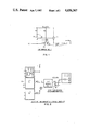
- FIG. 1 is the schematic diagram of the line charger or speed-up circuit in accordance with the invention.
- FIG. 2 is a block diagram of the line charger as employed in a typical logic gate configuration. It should be noted that the maximum benefit of the line charger is achieved when the line charger is physically located near the driving circuits.
- the capacitor pictured on the output of the line charger represents the land capacitance of the metal connecting the output of the driving circuits to the input of the load circuits.
- FIG. 3 discloses the simulated block diagram circuits employed to determine the delta in switching speed provided by the line charger.
- FIG. 4 discloses a plot showing the simulated response of TTL gates A and B (FIG. 3) to a falling transition.
- TTL gate B responded in time t.
- TTL gate A in cooperation with the line charger responded in time 0.3t.
- the speed-up circuit (line charger circuit) has its input connected to the collector dot output of three TTL circuits.
- the output of the line charger circuit is connected to the emitter input of a number of TTL circuits.
- the capacitor shown in FIG. 2 at the output of the line charger represents the high capacitance load attributable to the circuitry connected to the output of the line charger.
- the capacitor and the legend "capacitance of wiring (interconnecting metal)" represent the capacitive load on the output of the line charger circuit due to wiring and circuitry, such as logical circuits.
- the legend "Load/F.O.” load fan-out
- the circuitry such as logical circuits connected to the output of the line charger circuit.
- the up-going transition of TTL or DTL circuits is slow when applied to a high capacitive load. This effect turns out to be a major problem for VLSI logic chips.
- the circuit shown in FIG. 1 is an active pullup circuit to be connected between the output of the driving circuit and its load as shown in FIG. 2.
- the operation of the speed-up circuit is as follows. With the output of the TTL gate in FIG. 2 at a down level the components of the attached line charger as shown in FIG. 1 will be as follows.
- the base to emitter diode formed by transistor T1 will be forward biased clamping the voltage at node 1 to a V BE above the input voltage. Likewise, the base to emitter junction of transistor T3B will be forwarded biased causing T3B to operate in the saturated mode.
- the operation of the Line Charger while stimulated by an upgoing transition is as follows.
- the voltage at node 1 will rise along with the input voltage.
- the rising voltage at node 1 will activate transistor T2.
- the current conducted from collector to emitter of device T2 will charge the load capacitance connected to the output.
- Transistor T3B isolates the effect of the load capacitance at the output from the input during this transition.
- transistors T1 and T3B are forward biased and transistor T2 becomes inactive. With T3B active the load capacitance at the output is discharged and the output voltage falls to the low state.
- the circuit shown in FIG. 3 was simulated in order to compare the switching speed of a TTL gate with the aid of a line charger (gate A) and of a TTL gate without the aid of a line charger (gate B).
- the voltage at node 4 the output of gate B, FIG. 4 rose to the threshold voltage in time t after being stimulated by the input voltage at node 1.
- the output voltage of the line charger, node 3, FIG. 3 responded to the input stimulus in 0.3t.
- Transistor T2 charges the capacitive load very rapidly.
- Transistor T3B isolates the capacitive load on the output from the input, during the up-going transition.
- Transistor T1 and resistor R1 transfer the fast up-going transition of the input to the base of the driving transistor T2.
- the ⁇ line charger ⁇ is placed physically close to the driving TTL gate. Therefore, the input to the ⁇ line charger ⁇ is only lightly loaded and fast.
- the ⁇ line charger ⁇ circuit has an active up-going transition supported by T2, and an active down-going transition of the TTL circuit provided by T3B.
- Diode connected transistor T3A is used to reduce the inverse current in transistor T3B during saturation of T3B.
Landscapes
- Engineering & Computer Science (AREA)
- Physics & Mathematics (AREA)
- Computer Hardware Design (AREA)
- Computing Systems (AREA)
- General Engineering & Computer Science (AREA)
- Mathematical Physics (AREA)
- Power Engineering (AREA)
- Logic Circuits (AREA)
- Electronic Switches (AREA)
Priority Applications (5)
| Application Number | Priority Date | Filing Date | Title |
|---|---|---|---|
| US06/789,250 US4656367A (en) | 1985-10-18 | 1985-10-18 | Speed up of up-going transition of TTL or DTL circuits under high _capacitive load |
| CA000507289A CA1263716A (en) | 1985-10-18 | 1986-04-22 | Speed up of up-going transition of ttl or dtl circuits under high capacitive load |
| JP61209794A JPS6298914A (ja) | 1985-10-18 | 1986-09-08 | 高速集積回路チツプ |
| EP86113860A EP0219040B1 (de) | 1985-10-18 | 1986-10-07 | Schaltung zum Beschleunigen der ansteigenden Übergänge in TTL- oder DTL-Schaltungen mit hoher kapazitiver Belastung |
| DE8686113860T DE3676620D1 (de) | 1985-10-18 | 1986-10-07 | Schaltung zum beschleunigen der ansteigenden uebergaenge in ttl- oder dtl-schaltungen mit hoher kapazitiver belastung. |
Applications Claiming Priority (1)
| Application Number | Priority Date | Filing Date | Title |
|---|---|---|---|
| US06/789,250 US4656367A (en) | 1985-10-18 | 1985-10-18 | Speed up of up-going transition of TTL or DTL circuits under high _capacitive load |
Publications (1)
| Publication Number | Publication Date |
|---|---|
| US4656367A true US4656367A (en) | 1987-04-07 |
Family
ID=25147050
Family Applications (1)
| Application Number | Title | Priority Date | Filing Date |
|---|---|---|---|
| US06/789,250 Expired - Fee Related US4656367A (en) | 1985-10-18 | 1985-10-18 | Speed up of up-going transition of TTL or DTL circuits under high _capacitive load |
Country Status (5)
| Country | Link |
|---|---|
| US (1) | US4656367A (de) |
| EP (1) | EP0219040B1 (de) |
| JP (1) | JPS6298914A (de) |
| CA (1) | CA1263716A (de) |
| DE (1) | DE3676620D1 (de) |
Citations (17)
| Publication number | Priority date | Publication date | Assignee | Title |
|---|---|---|---|---|
| US3439186A (en) * | 1965-10-18 | 1969-04-15 | Motorola Inc | Diode transistor logic circuit having improved turn-on drive |
| US3457435A (en) * | 1965-12-21 | 1969-07-22 | Rca Corp | Complementary field-effect transistor transmission gate |
| US3491251A (en) * | 1965-12-20 | 1970-01-20 | Motorola Inc | Logic circuit having noise immunity capability which exceeds one-half the logic swing in both directions |
| US3560760A (en) * | 1970-02-02 | 1971-02-02 | Texas Instruments Inc | Logic nand gate circuits |
| US3576445A (en) * | 1968-04-01 | 1971-04-27 | Bell Telephone Labor Inc | Transistor logic arrangements |
| US3603816A (en) * | 1968-08-09 | 1971-09-07 | Bunker Ramo | High speed digital circuits |
| US3727081A (en) * | 1971-10-15 | 1973-04-10 | Motorola Inc | Regulator for controlling capacitor charge to provide complex waveform |
| US3867644A (en) * | 1974-01-07 | 1975-02-18 | Signetics Corp | High speed low power schottky integrated logic gate circuit with current boost |
| US4000429A (en) * | 1974-05-07 | 1976-12-28 | Tokyo Shibaura Electric Co., Ltd. | Semiconductor circuit device |
| US4070589A (en) * | 1976-10-29 | 1978-01-24 | The Singer Company | High speed-high voltage switching with low power consumption |
| US4071783A (en) * | 1976-11-29 | 1978-01-31 | International Business Machines Corporation | Enhancement/depletion mode field effect transistor driver |
| US4110637A (en) * | 1975-08-08 | 1978-08-29 | Ebauches S.A. | Electronic system for capacitively storing a signal voltage of predetermined level |
| US4137464A (en) * | 1976-03-26 | 1979-01-30 | International Business Machines Corporation | Charge-transfer binary search generating circuit |
| US4250411A (en) * | 1978-01-31 | 1981-02-10 | Siemens Aktiengesellschaft | Dynamic resistor current leakage compensation arrangement |
| US4344003A (en) * | 1980-08-04 | 1982-08-10 | Rca Corporation | Low power voltage multiplier circuit |
| US4424456A (en) * | 1979-12-26 | 1984-01-03 | Tokyo Shibaura Denki Kabushiki Kaisha | Driver circuit for charge coupled device |
| US4491748A (en) * | 1981-04-16 | 1985-01-01 | International Business Machines Corporation | High performance FET driver circuit |
Family Cites Families (4)
| Publication number | Priority date | Publication date | Assignee | Title |
|---|---|---|---|---|
| JPS555295B2 (de) * | 1971-09-10 | 1980-02-05 | ||
| DE2351128B2 (de) * | 1973-10-11 | 1976-05-20 | Siemens AG, 1000 Berlin und 8000 München | Schaltungsanordnung zum periodischen anschalten einer kapazitiven last an eine speisespannungsquelle |
| US4239981A (en) * | 1978-09-25 | 1980-12-16 | Ampex Corporation | Fast semiconductor digital logic inverter gate |
| US4458162A (en) * | 1981-07-10 | 1984-07-03 | International Business Machines Corporation | TTL Logic gate |
-
1985
- 1985-10-18 US US06/789,250 patent/US4656367A/en not_active Expired - Fee Related
-
1986
- 1986-04-22 CA CA000507289A patent/CA1263716A/en not_active Expired
- 1986-09-08 JP JP61209794A patent/JPS6298914A/ja active Granted
- 1986-10-07 EP EP86113860A patent/EP0219040B1/de not_active Expired
- 1986-10-07 DE DE8686113860T patent/DE3676620D1/de not_active Expired - Lifetime
Patent Citations (17)
| Publication number | Priority date | Publication date | Assignee | Title |
|---|---|---|---|---|
| US3439186A (en) * | 1965-10-18 | 1969-04-15 | Motorola Inc | Diode transistor logic circuit having improved turn-on drive |
| US3491251A (en) * | 1965-12-20 | 1970-01-20 | Motorola Inc | Logic circuit having noise immunity capability which exceeds one-half the logic swing in both directions |
| US3457435A (en) * | 1965-12-21 | 1969-07-22 | Rca Corp | Complementary field-effect transistor transmission gate |
| US3576445A (en) * | 1968-04-01 | 1971-04-27 | Bell Telephone Labor Inc | Transistor logic arrangements |
| US3603816A (en) * | 1968-08-09 | 1971-09-07 | Bunker Ramo | High speed digital circuits |
| US3560760A (en) * | 1970-02-02 | 1971-02-02 | Texas Instruments Inc | Logic nand gate circuits |
| US3727081A (en) * | 1971-10-15 | 1973-04-10 | Motorola Inc | Regulator for controlling capacitor charge to provide complex waveform |
| US3867644A (en) * | 1974-01-07 | 1975-02-18 | Signetics Corp | High speed low power schottky integrated logic gate circuit with current boost |
| US4000429A (en) * | 1974-05-07 | 1976-12-28 | Tokyo Shibaura Electric Co., Ltd. | Semiconductor circuit device |
| US4110637A (en) * | 1975-08-08 | 1978-08-29 | Ebauches S.A. | Electronic system for capacitively storing a signal voltage of predetermined level |
| US4137464A (en) * | 1976-03-26 | 1979-01-30 | International Business Machines Corporation | Charge-transfer binary search generating circuit |
| US4070589A (en) * | 1976-10-29 | 1978-01-24 | The Singer Company | High speed-high voltage switching with low power consumption |
| US4071783A (en) * | 1976-11-29 | 1978-01-31 | International Business Machines Corporation | Enhancement/depletion mode field effect transistor driver |
| US4250411A (en) * | 1978-01-31 | 1981-02-10 | Siemens Aktiengesellschaft | Dynamic resistor current leakage compensation arrangement |
| US4424456A (en) * | 1979-12-26 | 1984-01-03 | Tokyo Shibaura Denki Kabushiki Kaisha | Driver circuit for charge coupled device |
| US4344003A (en) * | 1980-08-04 | 1982-08-10 | Rca Corporation | Low power voltage multiplier circuit |
| US4491748A (en) * | 1981-04-16 | 1985-01-01 | International Business Machines Corporation | High performance FET driver circuit |
Non-Patent Citations (2)
| Title |
|---|
| I.B.M. Tech. Disc. Bul., vol. 26, No. 5, 10/83, "Compatible Circuits Implemented in DDL and TTL Technology". |
| I.B.M. Tech. Disc. Bul., vol. 26, No. 5, 10/83, Compatible Circuits Implemented in DDL and TTL Technology . * |
Also Published As
| Publication number | Publication date |
|---|---|
| EP0219040A3 (en) | 1987-07-01 |
| JPS6298914A (ja) | 1987-05-08 |
| JPH0563054B2 (de) | 1993-09-09 |
| CA1263716A (en) | 1989-12-05 |
| DE3676620D1 (de) | 1991-02-07 |
| EP0219040B1 (de) | 1990-12-27 |
| EP0219040A2 (de) | 1987-04-22 |
Similar Documents
| Publication | Publication Date | Title |
|---|---|---|
| KR910003597B1 (ko) | 데이터출력버퍼회로 및 전위변동 감축방법 | |
| US4813020A (en) | Semiconductor device | |
| US4948991A (en) | Load controlled ECL transient driver | |
| US4291242A (en) | Driver circuit for use in an output buffer | |
| KR840007326A (ko) | 반도체 직접회로 | |
| US4628218A (en) | Driving circuit suppressing peak value of charging current from power supply to capacitive load | |
| US4038567A (en) | Memory input signal buffer circuit | |
| US4689505A (en) | High speed bootstrapped CMOS driver | |
| EP0220870B1 (de) | Schnittstellenschaltung zur Umsetzung von ECL-Signalpegeln in FET-Logiksignalpegel | |
| US4937480A (en) | BICMOS buffer circuit | |
| US5157284A (en) | Integrated circuit including an input buffer circuit having nand and nor gates | |
| US4112314A (en) | Logical current switch | |
| JPH02222216A (ja) | BiCMOSドライバ回路 | |
| US4529895A (en) | Active high before open three state integrated circuit output stage | |
| US3604952A (en) | Tri-level voltage generator circuit | |
| EP0202582B1 (de) | NMOS-Datenspeicherzelle und Schieberegister | |
| US4081699A (en) | Depletion mode coupling device for a memory line driving circuit | |
| US3679917A (en) | Integrated circuit system having single power supply | |
| US5148048A (en) | CMOS output circuit having controlled slope | |
| GB2024550A (en) | Integrated driver circuits | |
| US4041333A (en) | High speed input buffer circuit | |
| US4656367A (en) | Speed up of up-going transition of TTL or DTL circuits under high _capacitive load | |
| KR0159324B1 (ko) | 데이터 출력회로 | |
| US3358154A (en) | High speed, low dissipation logic gates | |
| US4924116A (en) | Feedback source coupled FET logic |
Legal Events
| Date | Code | Title | Description |
|---|---|---|---|
| AS | Assignment |
Owner name: INTERNATIONAL BUSINESS MACHINES CORPORATION, ARMON Free format text: ASSIGNMENT OF ASSIGNORS INTEREST.;ASSIGNORS:CULICAN, EDWARD F.;PRITZLAFF, PHILIP E. JR.;SCHETTLER, HELMUT;AND OTHERS;REEL/FRAME:004479/0705;SIGNING DATES FROM 19850923 TO 19851016 |
|
| FPAY | Fee payment |
Year of fee payment: 4 |
|
| FPAY | Fee payment |
Year of fee payment: 8 |
|
| REMI | Maintenance fee reminder mailed | ||
| LAPS | Lapse for failure to pay maintenance fees | ||
| FP | Lapsed due to failure to pay maintenance fee |
Effective date: 19990407 |
|
| STCH | Information on status: patent discontinuation |
Free format text: PATENT EXPIRED DUE TO NONPAYMENT OF MAINTENANCE FEES UNDER 37 CFR 1.362 |