EP0219040A2 - Schaltung zum Beschleunigen der ansteigenden Übergänge in TTL- oder DTL-Schaltungen mit hoher kapazitiver Belastung - Google Patents
Schaltung zum Beschleunigen der ansteigenden Übergänge in TTL- oder DTL-Schaltungen mit hoher kapazitiver Belastung Download PDFInfo
- Publication number
- EP0219040A2 EP0219040A2 EP86113860A EP86113860A EP0219040A2 EP 0219040 A2 EP0219040 A2 EP 0219040A2 EP 86113860 A EP86113860 A EP 86113860A EP 86113860 A EP86113860 A EP 86113860A EP 0219040 A2 EP0219040 A2 EP 0219040A2
- Authority
- EP
- European Patent Office
- Prior art keywords
- transistor
- circuit
- collector
- base
- capacitive load
- Prior art date
- Legal status (The legal status is an assumption and is not a legal conclusion. Google has not performed a legal analysis and makes no representation as to the accuracy of the status listed.)
- Granted
Links
Images

Classifications
-
- H—ELECTRICITY
- H03—ELECTRONIC CIRCUITRY
- H03K—PULSE TECHNIQUE
- H03K19/00—Logic circuits, i.e. having at least two inputs acting on one output; Inverting circuits
- H03K19/02—Logic circuits, i.e. having at least two inputs acting on one output; Inverting circuits using specified components
- H03K19/08—Logic circuits, i.e. having at least two inputs acting on one output; Inverting circuits using specified components using semiconductor devices
- H03K19/082—Logic circuits, i.e. having at least two inputs acting on one output; Inverting circuits using specified components using semiconductor devices using bipolar transistors
- H03K19/088—Transistor-transistor logic
-
- H—ELECTRICITY
- H03—ELECTRONIC CIRCUITRY
- H03K—PULSE TECHNIQUE
- H03K19/00—Logic circuits, i.e. having at least two inputs acting on one output; Inverting circuits
- H03K19/01—Modifications for accelerating switching
- H03K19/013—Modifications for accelerating switching in bipolar transistor circuits
- H03K19/0136—Modifications for accelerating switching in bipolar transistor circuits by means of a pull-up or down element
Definitions
- the invention relates generally to circuits for digital equipment, and more particularly to circuitry for enhancing the ability of digital circuits to drive highly capacitive loads, especially for speeding up the up-going transitions occurring.
- the circuitry in accordance with the invention has particular utility when employed with logic circuits such as "TTL” (Tranistor-Transistor Logic) and "DTL” (Diode Transistor Logic).
- the up-going transition of TTL or DTL circuits employing passive pull-up circuit means is slow when applied to, or driving, a high capacitive load.
- This effect is a significant problem for VLSI logic chips.
- the invention may be summarized as a line charging, or speed-up, circuit the employment of which materially increases the speed with which a logic circuit, or the like, can drive, or charge-up a high capacitive load.
- the "speed-up" circuit includes transistor circuit means for rapidly charging the capacitive load and also transistor circuit means for isolating the input of the charging circuit from the output of the charging circuit during the up-going transition of an input signal, i.e. charging of the capacitive load.
- the charging circuit further includes means for aiding the discharge of the capacitive load during a down-level transition of an input signal.
- the up-going transition of TTL or DTL circuits is slow when applied to a high capacitive load. This effect turns out to be a major problem for VLSI logic chips.
- the circuit shown in figure 1 is an active pull-up circuit 15 to be connected between the output of the driving circuit 11, 12, 13 and its load 14 and the logic circuits 16 and connected to output node 3, as shown in figure 2.
- Capacitive load 14 may comprise the capacitance of the wiring as well as the input capacitance of said logic circuits.
- the operation of the speed-up circuit is as follows: With the output of the TTL gate 11, 12, 13 in figure 2 at a down level, the base-to-emitter diode formed by transistor Tl will be forwarded biased clamping the voltage at node 1 to a level V BE above the input voltage.
- the base-to-emitter junction of transistor T3B will be forward biased by a diode 10 causing it to operate in the saturated mode.
- the base-to-collector voltage of transistor T3B is integrated in parallel.
- the relation of the output voltage to the input voltage will be governed by the collector-to-emitter saturation voltage (V CE SAT) of transistor T3B.
- Transistor T2 will not be conducting current in this mode since the voltage from node 1 to the output node 3 is not great enough to forward bias the base-to-emitter junction of transistor T2.
- the operation of the Line Charger 15 of figure 1, while stimulated by an up-going transition is as follows: The voltage at node 1 will rise along with the input voltage. The rising voltage at node 1 will activate transistor T2. The current conducted from collector to emitter of transistor T2 will charge the load capacitance 14 connected to the output node 3. Transistor T3B isolates the effect of the load capacitance at output node 3 from input 5 during this transition.
- the circuit operation is as follows: The input voltage, node 1 and node 2 will have risen to the level of supply voltage to V C . Transistors Tl, T3A and T3B will be inactive. Transistor T2 will be forward biased clamping the output voltage to a level V BE below the supply voltage VC.
- transistors Tl and T3B are forward biased and transistor T2 becomes inactive. With transistor T3B active, the load capacitance at output node 3 is discharged and the output voltage falls to the low state.
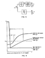
- the circuit shown in figure 3 was simulated in order to compare the switching speed of a TTL gate with the aid of a line charger (gate A) and of a TTL gate without the aid of a line charger (gate B).
- the voltage at node 4 the output voltage of gate B, figure 4 rose to the threshold voltage in a time t after having been stimulated by the input voltage at node 1.
- Transistor T2 charges the capacitive load 14 very rapidly.
- Transistor T3B isolates the capacitive load 14 on the output node 3 from the input 5, during the up-going transistor.
- Transistor Tl and resistor Rl transfer the fast up-going transition of the input voltage to the base of the driving transistor T2.
- the 'line charger' 15 is placed physically close to the driving TTL gate. Therefore, the input to the 'line charger' is only slightly loaded and fast.
- transistor T3B is on and connects the output node 3 to the input 5.
- the 'line charger' circuit has an active up-going transition supported by transistor T2, and an active down-going transition of the TTL circuit provided by transistor T3B.
- Diode-connected transistor T3A is used to reduce the inverse current in transistor T3B during the saturation thereof.
Landscapes
- Engineering & Computer Science (AREA)
- Physics & Mathematics (AREA)
- Computer Hardware Design (AREA)
- Computing Systems (AREA)
- General Engineering & Computer Science (AREA)
- Mathematical Physics (AREA)
- Power Engineering (AREA)
- Logic Circuits (AREA)
- Electronic Switches (AREA)
Applications Claiming Priority (2)
| Application Number | Priority Date | Filing Date | Title |
|---|---|---|---|
| US06/789,250 US4656367A (en) | 1985-10-18 | 1985-10-18 | Speed up of up-going transition of TTL or DTL circuits under high _capacitive load |
| US789250 | 1985-10-18 |
Publications (3)
| Publication Number | Publication Date |
|---|---|
| EP0219040A2 true EP0219040A2 (de) | 1987-04-22 |
| EP0219040A3 EP0219040A3 (en) | 1987-07-01 |
| EP0219040B1 EP0219040B1 (de) | 1990-12-27 |
Family
ID=25147050
Family Applications (1)
| Application Number | Title | Priority Date | Filing Date |
|---|---|---|---|
| EP86113860A Expired EP0219040B1 (de) | 1985-10-18 | 1986-10-07 | Schaltung zum Beschleunigen der ansteigenden Übergänge in TTL- oder DTL-Schaltungen mit hoher kapazitiver Belastung |
Country Status (5)
| Country | Link |
|---|---|
| US (1) | US4656367A (de) |
| EP (1) | EP0219040B1 (de) |
| JP (1) | JPS6298914A (de) |
| CA (1) | CA1263716A (de) |
| DE (1) | DE3676620D1 (de) |
Family Cites Families (21)
| Publication number | Priority date | Publication date | Assignee | Title |
|---|---|---|---|---|
| US3439186A (en) * | 1965-10-18 | 1969-04-15 | Motorola Inc | Diode transistor logic circuit having improved turn-on drive |
| US3491251A (en) * | 1965-12-20 | 1970-01-20 | Motorola Inc | Logic circuit having noise immunity capability which exceeds one-half the logic swing in both directions |
| US3457435A (en) * | 1965-12-21 | 1969-07-22 | Rca Corp | Complementary field-effect transistor transmission gate |
| US3576445A (en) * | 1968-04-01 | 1971-04-27 | Bell Telephone Labor Inc | Transistor logic arrangements |
| US3603816A (en) * | 1968-08-09 | 1971-09-07 | Bunker Ramo | High speed digital circuits |
| US3560760A (en) * | 1970-02-02 | 1971-02-02 | Texas Instruments Inc | Logic nand gate circuits |
| JPS555295B2 (de) * | 1971-09-10 | 1980-02-05 | ||
| US3727081A (en) * | 1971-10-15 | 1973-04-10 | Motorola Inc | Regulator for controlling capacitor charge to provide complex waveform |
| DE2351128B2 (de) * | 1973-10-11 | 1976-05-20 | Siemens AG, 1000 Berlin und 8000 München | Schaltungsanordnung zum periodischen anschalten einer kapazitiven last an eine speisespannungsquelle |
| US3867644A (en) * | 1974-01-07 | 1975-02-18 | Signetics Corp | High speed low power schottky integrated logic gate circuit with current boost |
| JPS50142128A (de) * | 1974-05-07 | 1975-11-15 | ||
| CH609200B (fr) * | 1975-08-08 | Ebauches Sa | Dispositif pour maintenir dans un etat determine le potentiel electrique d'un point d'un circuit electronique. | |
| GB1562774A (en) * | 1976-03-26 | 1980-03-19 | Ibm | Circuits for generating sequences of signals |
| US4070589A (en) * | 1976-10-29 | 1978-01-24 | The Singer Company | High speed-high voltage switching with low power consumption |
| US4071783A (en) * | 1976-11-29 | 1978-01-31 | International Business Machines Corporation | Enhancement/depletion mode field effect transistor driver |
| DE2804142C3 (de) * | 1978-01-31 | 1982-02-11 | Siemens AG, 1000 Berlin und 8000 München | Schaltungsanordnung zur Kompensation von Verlustströmen, die in einem zur Verstärkungsregelung von integrierten, breitbandigen Differenzverstärkern verwendeten dynamischen Widerstand durch parasitäre Transistoren bedingt sind |
| US4239981A (en) * | 1978-09-25 | 1980-12-16 | Ampex Corporation | Fast semiconductor digital logic inverter gate |
| EP0031583B1 (de) * | 1979-12-26 | 1988-08-17 | Kabushiki Kaisha Toshiba | Treiberschaltung für eine ladungsgekoppelte Vorrichtung |
| US4344003A (en) * | 1980-08-04 | 1982-08-10 | Rca Corporation | Low power voltage multiplier circuit |
| US4491748A (en) * | 1981-04-16 | 1985-01-01 | International Business Machines Corporation | High performance FET driver circuit |
| US4458162A (en) * | 1981-07-10 | 1984-07-03 | International Business Machines Corporation | TTL Logic gate |
-
1985
- 1985-10-18 US US06/789,250 patent/US4656367A/en not_active Expired - Fee Related
-
1986
- 1986-04-22 CA CA000507289A patent/CA1263716A/en not_active Expired
- 1986-09-08 JP JP61209794A patent/JPS6298914A/ja active Granted
- 1986-10-07 EP EP86113860A patent/EP0219040B1/de not_active Expired
- 1986-10-07 DE DE8686113860T patent/DE3676620D1/de not_active Expired - Lifetime
Also Published As
| Publication number | Publication date |
|---|---|
| EP0219040A3 (en) | 1987-07-01 |
| JPS6298914A (ja) | 1987-05-08 |
| JPH0563054B2 (de) | 1993-09-09 |
| CA1263716A (en) | 1989-12-05 |
| DE3676620D1 (de) | 1991-02-07 |
| EP0219040B1 (de) | 1990-12-27 |
| US4656367A (en) | 1987-04-07 |
Similar Documents
| Publication | Publication Date | Title |
|---|---|---|
| US4948991A (en) | Load controlled ECL transient driver | |
| US4638186A (en) | BIMOS logic gate | |
| KR840007326A (ko) | 반도체 직접회로 | |
| US4605870A (en) | High speed low power current controlled gate circuit | |
| US4112314A (en) | Logical current switch | |
| JPH02222216A (ja) | BiCMOSドライバ回路 | |
| US5132564A (en) | Bus driver circuit with low on-chip dissipation and/or pre-biasing of output terminal during live insertion | |
| US4593205A (en) | Macrocell array having an on-chip clock generator | |
| US4623803A (en) | Logic level translator circuit for integrated circuit semiconductor devices having transistor-transistor logic output circuitry | |
| US3778640A (en) | Signal voltage level translating circuit | |
| US4675555A (en) | IC input buffer emitter follower with current source value dependent upon connection length for equalizing signal delay | |
| US3358154A (en) | High speed, low dissipation logic gates | |
| EP0046498B1 (de) | Bootstrap-Treiberschaltung | |
| US4531067A (en) | Push-pull Darlington current sink (PPDCS) logic circuit | |
| US5124582A (en) | Bi-cmos circuit with high-speed active pull-down output currents | |
| EP0219040A2 (de) | Schaltung zum Beschleunigen der ansteigenden Übergänge in TTL- oder DTL-Schaltungen mit hoher kapazitiver Belastung | |
| US5066874A (en) | Signal output circuit having bipolar transistor in output stage and arranged in cmos semiconductor integrated circuit | |
| US4459496A (en) | Semiconductor integrated circuit having stacked integrated injection logic circuits | |
| US3452216A (en) | Logic circuit | |
| US4709167A (en) | Three-state output buffer with anti-saturation control | |
| US4749885A (en) | Nonsaturating bipolar logic gate having a low number of components and low power dissipation | |
| US4570240A (en) | AC Transient driver for memory cells | |
| KR890016769A (ko) | 바이폴라트랜지스터와 mosfet의 복합으로 형성된 논리회로 | |
| EP0285068A3 (de) | Logikschaltung | |
| US4947058A (en) | TTL current sinking circuit with transient performance enhancement during output transition from high to low |
Legal Events
| Date | Code | Title | Description |
|---|---|---|---|
| PUAI | Public reference made under article 153(3) epc to a published international application that has entered the european phase |
Free format text: ORIGINAL CODE: 0009012 |
|
| AK | Designated contracting states |
Kind code of ref document: A2 Designated state(s): DE FR GB IT |
|
| PUAL | Search report despatched |
Free format text: ORIGINAL CODE: 0009013 |
|
| AK | Designated contracting states |
Kind code of ref document: A3 Designated state(s): DE FR GB IT |
|
| 17P | Request for examination filed |
Effective date: 19870821 |
|
| 17Q | First examination report despatched |
Effective date: 19890321 |
|
| GRAA | (expected) grant |
Free format text: ORIGINAL CODE: 0009210 |
|
| AK | Designated contracting states |
Kind code of ref document: B1 Designated state(s): DE FR GB IT |
|
| PG25 | Lapsed in a contracting state [announced via postgrant information from national office to epo] |
Ref country code: IT Free format text: LAPSE BECAUSE OF FAILURE TO SUBMIT A TRANSLATION OF THE DESCRIPTION OR TO PAY THE FEE WITHIN THE PRESCRIBED TIME-LIMIT;WARNING: LAPSES OF ITALIAN PATENTS WITH EFFECTIVE DATE BEFORE 2007 MAY HAVE OCCURRED AT ANY TIME BEFORE 2007. THE CORRECT EFFECTIVE DATE MAY BE DIFFERENT FROM THE ONE RECORDED. Effective date: 19901227 |
|
| REF | Corresponds to: |
Ref document number: 3676620 Country of ref document: DE Date of ref document: 19910207 |
|
| ET | Fr: translation filed | ||
| PLBE | No opposition filed within time limit |
Free format text: ORIGINAL CODE: 0009261 |
|
| STAA | Information on the status of an ep patent application or granted ep patent |
Free format text: STATUS: NO OPPOSITION FILED WITHIN TIME LIMIT |
|
| 26N | No opposition filed | ||
| PGFP | Annual fee paid to national office [announced via postgrant information from national office to epo] |
Ref country code: GB Payment date: 19950926 Year of fee payment: 10 |
|
| PGFP | Annual fee paid to national office [announced via postgrant information from national office to epo] |
Ref country code: FR Payment date: 19951009 Year of fee payment: 10 |
|
| PGFP | Annual fee paid to national office [announced via postgrant information from national office to epo] |
Ref country code: DE Payment date: 19951030 Year of fee payment: 10 |
|
| PG25 | Lapsed in a contracting state [announced via postgrant information from national office to epo] |
Ref country code: GB Effective date: 19961007 |
|
| GBPC | Gb: european patent ceased through non-payment of renewal fee |
Effective date: 19961007 |
|
| PG25 | Lapsed in a contracting state [announced via postgrant information from national office to epo] |
Ref country code: FR Effective date: 19970630 |
|
| PG25 | Lapsed in a contracting state [announced via postgrant information from national office to epo] |
Ref country code: DE Effective date: 19970701 |
|
| REG | Reference to a national code |
Ref country code: FR Ref legal event code: ST |