US4549788A - Intensity of a light beam applied to a layered semiconductor structure controls the beam - Google Patents
Intensity of a light beam applied to a layered semiconductor structure controls the beam Download PDFInfo
- Publication number
- US4549788A US4549788A US06/455,461 US45546183A US4549788A US 4549788 A US4549788 A US 4549788A US 45546183 A US45546183 A US 45546183A US 4549788 A US4549788 A US 4549788A
- Authority
- US
- United States
- Prior art keywords
- layers
- interface
- charge
- light beam
- energy band
- Prior art date
- Legal status (The legal status is an assumption and is not a legal conclusion. Google has not performed a legal analysis and makes no representation as to the accuracy of the status listed.)
- Expired - Lifetime
Links
- 239000004065 semiconductor Substances 0.000 title claims abstract description 24
- 230000003287 optical effect Effects 0.000 claims abstract description 81
- 239000000463 material Substances 0.000 claims description 94
- 230000035515 penetration Effects 0.000 claims description 2
- 230000007423 decrease Effects 0.000 description 7
- 239000007787 solid Substances 0.000 description 6
- 238000010586 diagram Methods 0.000 description 4
- 229910001218 Gallium arsenide Inorganic materials 0.000 description 3
- 230000001419 dependent effect Effects 0.000 description 3
- 230000005374 Kerr effect Effects 0.000 description 2
- 230000005540 biological transmission Effects 0.000 description 2
- 239000000758 substrate Substances 0.000 description 2
- 238000010521 absorption reaction Methods 0.000 description 1
- 229910045601 alloy Inorganic materials 0.000 description 1
- 239000000956 alloy Substances 0.000 description 1
- 239000000969 carrier Substances 0.000 description 1
- 230000003247 decreasing effect Effects 0.000 description 1
- 239000007789 gas Substances 0.000 description 1
- 239000007788 liquid Substances 0.000 description 1
- 230000000737 periodic effect Effects 0.000 description 1
- 238000002310 reflectometry Methods 0.000 description 1
- 239000011343 solid material Substances 0.000 description 1
- 238000001228 spectrum Methods 0.000 description 1
- 230000005428 wave function Effects 0.000 description 1
Images


Classifications
-
- G—PHYSICS
- G02—OPTICS
- G02F—OPTICAL DEVICES OR ARRANGEMENTS FOR THE CONTROL OF LIGHT BY MODIFICATION OF THE OPTICAL PROPERTIES OF THE MEDIA OF THE ELEMENTS INVOLVED THEREIN; NON-LINEAR OPTICS; FREQUENCY-CHANGING OF LIGHT; OPTICAL LOGIC ELEMENTS; OPTICAL ANALOGUE/DIGITAL CONVERTERS
- G02F1/00—Devices or arrangements for the control of the intensity, colour, phase, polarisation or direction of light arriving from an independent light source, e.g. switching, gating or modulating; Non-linear optics
- G02F1/35—Non-linear optics
- G02F1/3511—Self-focusing or self-trapping of light; Light-induced birefringence; Induced optical Kerr-effect
-
- B—PERFORMING OPERATIONS; TRANSPORTING
- B82—NANOTECHNOLOGY
- B82Y—SPECIFIC USES OR APPLICATIONS OF NANOSTRUCTURES; MEASUREMENT OR ANALYSIS OF NANOSTRUCTURES; MANUFACTURE OR TREATMENT OF NANOSTRUCTURES
- B82Y20/00—Nanooptics, e.g. quantum optics or photonic crystals
-
- G—PHYSICS
- G02—OPTICS
- G02F—OPTICAL DEVICES OR ARRANGEMENTS FOR THE CONTROL OF LIGHT BY MODIFICATION OF THE OPTICAL PROPERTIES OF THE MEDIA OF THE ELEMENTS INVOLVED THEREIN; NON-LINEAR OPTICS; FREQUENCY-CHANGING OF LIGHT; OPTICAL LOGIC ELEMENTS; OPTICAL ANALOGUE/DIGITAL CONVERTERS
- G02F1/00—Devices or arrangements for the control of the intensity, colour, phase, polarisation or direction of light arriving from an independent light source, e.g. switching, gating or modulating; Non-linear optics
- G02F1/01—Devices or arrangements for the control of the intensity, colour, phase, polarisation or direction of light arriving from an independent light source, e.g. switching, gating or modulating; Non-linear optics for the control of the intensity, phase, polarisation or colour
- G02F1/015—Devices or arrangements for the control of the intensity, colour, phase, polarisation or direction of light arriving from an independent light source, e.g. switching, gating or modulating; Non-linear optics for the control of the intensity, phase, polarisation or colour based on semiconductor elements having potential barriers, e.g. having a PN or PIN junction
- G02F1/017—Structures with periodic or quasi periodic potential variation, e.g. superlattices, quantum wells
- G02F1/01716—Optically controlled superlattice or quantum well devices
Definitions
- the invention relates to an arrangement for controlling a beam of light and more particularly to an arrangement including a layered semiconductor structure for controlling an input beam by varying the intensity of the beam.
- nonlinear optical materials In various arrangements, gases, liquids, and solids have been used as nonlinear optical materials.
- an optical device including a layered semiconductor structure having a variable input light beam applied to the structure with an E field component polarized normal to the layers. Intensity of the input light beam controls charge trapped in the layers, the dielectric constant of the layers containing the trapped charge, and the propagation of the input light beam within the device.
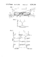
- FIG. 1 is a schematic diagram of an optical device embodying the invention
- FIG. 2 is a characteristic curve for the device of FIG. 1;
- FIG. 3 is a cross-section of a layered structure together with two different charge density function curves that occur under certain operating conditions
- FIG. 4 is a schematic diagram of another optical device embodying the invention.
- FIGS. 5, 6 and 7 are a group of operating characteristic curves for the device of FIG. 4;
- FIG. 8 is a schematic diagram of still another optical device embodying the invention.
- FIG. 9 is a schematic diagram of a further optical device embodying the invention.
- an optical device 10 is a nonlinear switching arrangement including an optical interface 12 between a linear optical material 14 and a nonlinear optical material 16.
- the linear optical material 14 is a solid substrate material, such as a semiconductor material.
- Ga 1-x Al x As is an alloy system from which a suitable linear optical material can be selected.
- the linear optical material 14 has an index of refraction n o .
- the nonlinear optical material 16 is a layered semiconductor structure containing alternate layers of small energy band gap material 18 and a large energy band gap material 19. The layers of materials are lattice matched with the substrate.
- One type of layered semiconductor material is a multiple quantum well structure that includes layers of GaAs as the material 18 and layers of Ga 1-x Al x As as the material 19.
- I is the intensity of the input beam
- n 1 is the zero-intensity refractive index
- n 2 is the optical Kerr coefficient.
- a superlattice structure Another type of suitable layered semiconductor material is called a superlattice structure. It is a special case of the just described multiple quantum well structure wherein the layers are periodic with a period of the order of a few hundred Angstroms.
- the structure is designed for trapping a predetermined quantity of charge in the layers of small energy band gap material 18.
- the layers 18 are extrinsic semiconductor layers, such as GaAs, illustratively doped with n-type carriers leaving a predetermined quantity of trapped charge in those layers 18 while the material is not energized externally.
- a wave function of the trapped charge in the layers 18 is an oscillating sine waveform.
- An intrinsic semiconductor, such as Ga 1-x Al x As, is formed into the layers of large energy band gap material 19 which are thick enough so that the trapped charge in any layer 18 is isolated from the charge in every other layer 18. Any trapped charge which spreads into the layers 19, decreases exponentially therein.
- the trapped charge penetrates into the layers 19 on the order of 10 to 20 angstroms. With the layers 19 being 5-10 times thicker than the penetration of the trapped charge, each layer 18 operates as an independent square well.
- a variable input beam source 20 of monochromatic light produces a polarized light beam 21 that is applied to the optical device 10.
- This input light beam is directed through the layered nonlinear optical material to the optical interface 12 between the nonlinear optical material 16 and the linear optical material 14.
- the input light beam 21 is directed along an axis which is positioned at an angle of incidence ⁇ that is greater than the critical angle of incidence for low intensity light and is less than the critical angle of incidence for high intensity light.
- the input light beam 21 has an E field component 22 that is polarized normal to the layers of the multiple quantum well structure for reasons to be presented subsequently.
- the source 20 is arranged to vary the intensity I of the input light beam 21.
- the reflectivity of the interface 12 is intensity dependent.
- the source of light 20 produces a beam of light having an intensity which can be varied through a range of intensities.
- an effective critical angle of incidence is greater than the angle of incidence ⁇ and the beam is totally internally reflected at the interface.
- the reflected beam 23 is reflected from the interface through the layered nonlinear optical material 16 to an optical detector 28. No beam is transmitted through the linear material 14.
- the effective critical angle equals the angle of incidence ⁇ .
- the total internal reflection switches to nearly total transmission of the input beam through the interface 12 into and through the linear optical material 14.
- the effective critical angle is less than the angle of incidence ⁇ and the beam traverses the multiple quantum well structure and the optical interface 12. Then the transmitted output beam 25 is transmitted through the linear optical material 14 away from the detector 28.
- the detector 28 of FIG. 1 determines whether the intensity of the input light beam is above or below the critical intensity I c . As shown by the solid curve 30 in FIG. 2, for input beam intensities below the critical intensity I c , the detector receives most of the light from the input beam and indicates a high output beam intensity. When the input beam intensity is approximately equal to the critical intensity I c , the output beam applied to the detector has a rapidly falling intensity. For input beam intensities above the critical intensity I c , the output beam applied to the detector is a low intensity.
- the dotted curve 34 in FIG. 2 represents the operating characteristic of the arrangement of FIG. 1 when the detector is positioned in an alternate position shown by a dotted detector 29.
- FIG. 3 there are shown a pair of charge distribution curves 31 and 32 which are associated with a layered structure 35 like the layered structure 16 of FIG. 1.
- the layered structure 35 contains trapped charge which is shown illustratively as minus signs in the layered structure. As shown the charge is concentrated within layers of small energy band gap material 38. Some of this charge penetrates slightly into layers of large energy band gap material 39.
- FIG. 3 shows only negative charge, a device similar to device 10 can be made and operated with positive trapped charge.
- the density of the charge in the layers is distributed symmetrically, as shown by the curve 31.
- Most of the charge is trapped in the layers 38, as shown by the peaks in curve 31 and by the density of minus signs in the layers 38 of the structure 35.
- a small portion spills over into the adjacent regions of the layers 39, as shown in the lower portions of the peaks in curve 31 and by the scattered minus signs in the layers 39 of the structure 35.
- the semiconductor layers 39 are thick enough to isolate the charge of each separate layer 38. Thus the charge is trapped in the layers of small energy band gap material 38.
- the optical device either nearly totally reflects the input beam to the detector 28 or else transmits most of it through the linear material away from the detector.
- control of the incident light beam at the interface between the layered semiconductor structure and the linear material is dependent upon the intensity of the input beam itself.
- K is the number of elementary tubes per unit volume.
- K also equals the number of elementary tubes per unit of surface times the number of layers 19 per unit of length.
- d 2 is the thickness of the layer 19.
- N e typically has a value in the range from 10 17 to 3 ⁇ 10 17 . With a value for N e selected within that range, the device 10 of FIG. 1 would have a nonlinearity x.sup.(3) in a range between 2 ⁇ 10 -4 esu and 8 ⁇ 10 -5 esu.
- the operative phenomenon is a dynamic movement of the trapped charge in response to changes of intensity of the input beam of light, the speed of operation potentially is very high.
- a layered nonlinear optical material 41 such as a multiple quantum well structure, forms an optical interface with a linear optical material 42 similar to the arrangement of FIG. 1 except that charge is not doped into the layers of small energy band gap material 48 of the layered nonlinear optical material 41. Instead a light source 45 produces a charge energizing beam 46 which is directed into the layered structure where it is absorbed for creating charge in the layers 48. As long as the beam 46 is applied, the charge is trapped in those layers 48.
- FIG. 5 shows a plot of the charge density in the layers 48 in response to the intensity of the charge energizing beam 46.
- a variable input beam light source 50 produces a monochromatic light beam 51 which is applied to the optical interface between the linear and nonlinear optical materials at an angle of incidence ⁇ which is larger than the effective critical angle for high intensity beams and smaller than the effective critical angle for low intensity beams.
- the input beam 51 traverses the optical interface and is transmitted on through the layered nonlinear optical material 41 away from a detector 53.
- the intensity of the input beam 51 is varied from a low value to a high value, the dielectric constant and the refractive index n of the layered material change as a result of the optical Kerr effect.
- the effective critical angle of the input beam equals the angle of incidence ⁇ and the nearly total transmission switches to internal reflection.
- the effective critical angle is larger than the angle of incidence ⁇ and the beam 51 is entirely internally reflected along a path 52 to the optical detector 53.
- FIG. 7 there is shown an operating characteristic for the device 40 of FIG. 4.
- the solid curve 71 represents the operating function when the detector 53 is positioned as shown in FIG. 4.
- the dotted characteristic curve 72 also shown in FIG. 7, represents the characteristic curve which is applicable to the arrangement of FIG. 4 with the detector positioned, as shown by an alternative detector 55 that is dotted in FIG. 4.
- the charge beam source 45 is shown in FIG. 4 as applying the charge energizing beam 46 incident upon the upper surface of the layered material.
- the charge beam source 45 can be positioned to apply the charge energizing beam to the lower surface of the linear material so long as the beam penetrates to the layered material for generating the desired trapped charge.
- the charge energizing beam has a wavelength in a range of 0.6-0.9 micrometers.
- FIGS. 8 and 9 there are shown other arrangements of nonlinear optical devices using layered semiconductor structures.
- FIG. 8 there is an optical device arrangement 80 including a linear optical material 81 and a layered nonlinear optical material 82 wherein the refractive index n o of the linear optical material is larger than the zero-intensity input beam refractive index n 1 of the layered nonlinear material.
- Charge is doped into the layers 84 as described with respect to the embodiment of FIG. 1.
- the monochromatic input beam 83 is applied through the linear optical material to the optical interface at an angle of incidence ⁇ exceeding the effective critical angle of incidence for high intensity light and smaller than the effective critical angle for low intensity light. For low intensities of the input beam, it is transmitted on through the layered nonlinear material 82 away from a detector 85.
- the refractive index of the nonlinear media decreases and the effective critical angle decreases.
- the input light beam 83 is totally internally reflected.
- a characteristic curve similar to the solid curve 71 in FIG. 7 results.
- the dotted characteristic curve 72 of FIG. 7 applies to the operation of the device 80 in FIG. 8 when the detector is placed in the alternate position of detector 87, shown dotted, in FIG. 8.
- the device 80 operates effectively in a wavelength range above 0.85 micrometers.
- FIG. 9 there is an optical device arrangement 90 including a linear optical material 91 and a layered nonlinear optical material 92 wherein the refractive index n o of the linear optical material is less than the zero-intensity input beam refractive index n 1 of the layered nonlinear material.
- Charge is generated in the layers of the layered nonlinear optical material 92 by a charge energizing light beam from a charge beam source 93, as in the arrangement described with respect to FIG. 4.
- the monochromatic input beam 94 is applied through the layered nonlinear optical material to the interface at an angle of incidence ⁇ exceeding the critical angle of incidence for low intensity light.
- the input beam 94 is totally internally reflected to the detector 96 for low intensities of the input beam.
- a resulting characteristic curve is similar to the solid curve shown in FIG. 2.
- the dotted characteristic curve of FIG. 2 applies to the device shown in FIG. 9 when the detector is placed in the alternate position of detector 98, shown dotted in FIG. 9.
- devices operating in accordance with the prior discussion can perform in a wide range of wavelengths.
- devices fabricated in the mentioned material system provide devices for wavelengths of the input beam larger than 0.85 micrometers and for wavelengths of the charge energizing beam in a range of 0.6-0.9 micrometers.
- the resulting devices can be operated with the wavelength of the input beam larger than 1.3 and 1.5 micrometers, respectively, and with the wavelength of the energizing beam in a range of 1.0-1.5 micrometers.
- the materials may be selected from either of the material systems.
- trapped positive charge may be provided by doping the layers of the low energy band gap material or by energizing the charge optically.
Landscapes
- Physics & Mathematics (AREA)
- Nonlinear Science (AREA)
- Optics & Photonics (AREA)
- General Physics & Mathematics (AREA)
- Chemical & Material Sciences (AREA)
- Engineering & Computer Science (AREA)
- Nanotechnology (AREA)
- Life Sciences & Earth Sciences (AREA)
- Biophysics (AREA)
- Crystallography & Structural Chemistry (AREA)
- Photo Coupler, Interrupter, Optical-To-Optical Conversion Devices (AREA)
- Optical Modulation, Optical Deflection, Nonlinear Optics, Optical Demodulation, Optical Logic Elements (AREA)
Priority Applications (6)
| Application Number | Priority Date | Filing Date | Title |
|---|---|---|---|
| US06/455,461 US4549788A (en) | 1983-01-03 | 1983-01-03 | Intensity of a light beam applied to a layered semiconductor structure controls the beam |
| JP84500712A JPS60500231A (ja) | 1983-01-03 | 1983-12-29 | 層状半導体構造に与えられる光ビ−ムの強度が該ビ−ムを制御する |
| EP84900582A EP0131042B1 (de) | 1983-01-03 | 1983-12-29 | Die intensität eines lichtstrahls gerichtet auf eine integrierte schaltung steuert den strahl |
| PCT/US1983/002054 WO1984002783A1 (en) | 1983-01-03 | 1983-12-29 | Intensity of a light beam applied to a layered semiconductor structure controls the beam |
| DE8484900582T DE3382289D1 (de) | 1983-01-03 | 1983-12-29 | Die intensitaet eines lichtstrahls gerichtet auf eine integrierte schaltung steuert den strahl. |
| CA000444492A CA1206575A (en) | 1983-01-03 | 1983-12-30 | Light beam director utilizing variation of beam intensity impinging on layered semiconductor structure |
Applications Claiming Priority (1)
| Application Number | Priority Date | Filing Date | Title |
|---|---|---|---|
| US06/455,461 US4549788A (en) | 1983-01-03 | 1983-01-03 | Intensity of a light beam applied to a layered semiconductor structure controls the beam |
Publications (1)
| Publication Number | Publication Date |
|---|---|
| US4549788A true US4549788A (en) | 1985-10-29 |
Family
ID=23808897
Family Applications (1)
| Application Number | Title | Priority Date | Filing Date |
|---|---|---|---|
| US06/455,461 Expired - Lifetime US4549788A (en) | 1983-01-03 | 1983-01-03 | Intensity of a light beam applied to a layered semiconductor structure controls the beam |
Country Status (6)
| Country | Link |
|---|---|
| US (1) | US4549788A (de) |
| EP (1) | EP0131042B1 (de) |
| JP (1) | JPS60500231A (de) |
| CA (1) | CA1206575A (de) |
| DE (1) | DE3382289D1 (de) |
| WO (1) | WO1984002783A1 (de) |
Cited By (11)
| Publication number | Priority date | Publication date | Assignee | Title |
|---|---|---|---|---|
| US4737003A (en) * | 1983-12-23 | 1988-04-12 | Hitachi, Ltd. | Optical switching device utilizing multiple quantum well structures between intersecting waveguides |
| US4761620A (en) * | 1986-12-03 | 1988-08-02 | American Telephone And Telegraph Company, At&T Bell Laboratories | Optical reading of quantum well device |
| US4784476A (en) * | 1987-01-27 | 1988-11-15 | Hughes Aircraft Company | Nipi refractive index modulation apparatus and method |
| US4828368A (en) * | 1986-06-30 | 1989-05-09 | Hughes Aircraft Company | Near bandgap radiation modulation spatial light modulators |
| US4829269A (en) * | 1987-09-17 | 1989-05-09 | Spectrolab, Inc. | Harmonic plasma switch |
| US4851840A (en) * | 1988-01-06 | 1989-07-25 | Wright State University | Optical analog to digital converter |
| US4863245A (en) * | 1984-02-28 | 1989-09-05 | Exxon Research And Engineering Company | Superlattice electrooptic devices |
| US4872744A (en) * | 1988-01-15 | 1989-10-10 | Bell Communications Research, Inc. | Single quantum well optical modulator |
| US5005933A (en) * | 1988-09-30 | 1991-04-09 | Canon Kabushiki Kaisha | Non-linear optical device |
| US5016990A (en) * | 1988-02-12 | 1991-05-21 | U.S. Philips Corp. | Method of modulating an optical beam |
| US5986828A (en) * | 1988-11-01 | 1999-11-16 | The United States Of America As Represented By The Secretary Of The Army | Optical power limiter utilizing nonlinear refraction |
Families Citing this family (3)
| Publication number | Priority date | Publication date | Assignee | Title |
|---|---|---|---|---|
| JPH0834479B2 (ja) * | 1987-10-22 | 1996-03-29 | 国際電信電話株式会社 | 光パケット交換方式 |
| JPH0769549B2 (ja) * | 1987-10-22 | 1995-07-31 | 国際電信電話株式会社 | 光駆動形スイッチ |
| US5004325A (en) * | 1990-01-16 | 1991-04-02 | At&T Bell Laboratories | Optical processing using a multilayer heterostructure |
Citations (2)
| Publication number | Priority date | Publication date | Assignee | Title |
|---|---|---|---|---|
| US3746879A (en) * | 1972-05-25 | 1973-07-17 | Ibm | Superlattice harmonic generator & mixer for electromagnetic waves |
| US4190811A (en) * | 1975-05-22 | 1980-02-26 | Canadian Patents And Development Limited | Laser controlled optical switching in semiconductors |
-
1983
- 1983-01-03 US US06/455,461 patent/US4549788A/en not_active Expired - Lifetime
- 1983-12-29 EP EP84900582A patent/EP0131042B1/de not_active Expired
- 1983-12-29 JP JP84500712A patent/JPS60500231A/ja active Granted
- 1983-12-29 DE DE8484900582T patent/DE3382289D1/de not_active Expired - Fee Related
- 1983-12-29 WO PCT/US1983/002054 patent/WO1984002783A1/en active IP Right Grant
- 1983-12-30 CA CA000444492A patent/CA1206575A/en not_active Expired
Patent Citations (2)
| Publication number | Priority date | Publication date | Assignee | Title |
|---|---|---|---|---|
| US3746879A (en) * | 1972-05-25 | 1973-07-17 | Ibm | Superlattice harmonic generator & mixer for electromagnetic waves |
| US4190811A (en) * | 1975-05-22 | 1980-02-26 | Canadian Patents And Development Limited | Laser controlled optical switching in semiconductors |
Non-Patent Citations (18)
| Title |
|---|
| Gibbs et al., "Optical Bistability in Semiconductors", App. Phys. Letts., 9-1979, pp. 451-453. |
| Gibbs et al., "Room-Temperature Excitonic Optical Bistability in a GaAs-GaAlAs Superlattice Etalon", Applied Physics Lett., 8-1-1982, pp. 221-222. |
| Gibbs et al., Optical Bistability in Semiconductors , App. Phys. Letts., 9 1979, pp. 451 453. * |
| Gibbs et al., Room Temperature Excitonic Optical Bistability in a GaAs GaAlAs Superlattice Etalon , Applied Physics Lett., 8 1 1982, pp. 221 222. * |
| Kaplan, A. E., "Theory of Hysteresis Reflection & Refraction of Light by a Boundry of a Nonlinear Medium", Sov. Phys., JETP 45(5) 5-1977, pp. 896-905. |
| Kaplan, A. E., Theory of Hysteresis Reflection & Refraction of Light by a Boundry of a Nonlinear Medium , Sov. Phys., JETP 45(5) 5 1977, pp. 896 905. * |
| Miller et al., "Large Room-Temperature Optical Nonlinearity in GaAs/Ga1-4 Al4 As Multiple Quantum Well Structures", App. Phys. Lett. 41(8) 10-1982, pp. 679-681. |
| Miller et al., Large Room Temperature Optical Nonlinearity in GaAs/Ga 1 4 Al 4 As Multiple Quantum Well Structures , App. Phys. Lett. 41(8) 10 1982, pp. 679 681. * |
| Reinhart et al., "Efficient GaAs-Alx Ga1-x As Double-Heterstructure Light Modulators", App. Phys. Lett., 1-1972, pp. 36-38. |
| Reinhart et al., Efficient GaAs Al x Ga 1 x As Double Heterstructure Light Modulators , App. Phys. Lett., 1 1972, pp. 36 38. * |
| Smith et al., "Bistable Optical Devices Promise Subpicosecond Switching", IEEE Spectrum 6-1981, pp. 26-31. |
| Smith et al., "Experimental Studies of a nonlinear Interface", IEEE Jr. of Quantum Electronics, vol. 17, 3-1981, pp. 340-348. |
| Smith et al., Bistable Optical Devices Promise Subpicosecond Switching , IEEE Spectrum 6 1981, pp. 26 31. * |
| Smith et al., Experimental Studies of a nonlinear Interface , IEEE Jr. of Quantum Electronics, vol. 17, 3 1981, pp. 340 348. * |
| Streifer et al., "Optical Analysis of Multiple-Quantum-Well Lasers", App. Optics, 11-1979, pp. 3547-3548. |
| Streifer et al., Optical Analysis of Multiple Quantum Well Lasers , App. Optics, 11 1979, pp. 3547 3548. * |
| Van Der Ziel et al., "Laser Oscillation from Quantum States in Very Thin GaAs-Al0.2 Ga0.8 s Multilayer Structures", App. Phys. Lett. 4-1975, pp. 463-465. |
| Van Der Ziel et al., Laser Oscillation from Quantum States in Very Thin GaAs Al 0.2 Ga 0.8 s Multilayer Structures , App. Phys. Lett. 4 1975, pp. 463 465. * |
Cited By (11)
| Publication number | Priority date | Publication date | Assignee | Title |
|---|---|---|---|---|
| US4737003A (en) * | 1983-12-23 | 1988-04-12 | Hitachi, Ltd. | Optical switching device utilizing multiple quantum well structures between intersecting waveguides |
| US4863245A (en) * | 1984-02-28 | 1989-09-05 | Exxon Research And Engineering Company | Superlattice electrooptic devices |
| US4828368A (en) * | 1986-06-30 | 1989-05-09 | Hughes Aircraft Company | Near bandgap radiation modulation spatial light modulators |
| US4761620A (en) * | 1986-12-03 | 1988-08-02 | American Telephone And Telegraph Company, At&T Bell Laboratories | Optical reading of quantum well device |
| US4784476A (en) * | 1987-01-27 | 1988-11-15 | Hughes Aircraft Company | Nipi refractive index modulation apparatus and method |
| US4829269A (en) * | 1987-09-17 | 1989-05-09 | Spectrolab, Inc. | Harmonic plasma switch |
| US4851840A (en) * | 1988-01-06 | 1989-07-25 | Wright State University | Optical analog to digital converter |
| US4872744A (en) * | 1988-01-15 | 1989-10-10 | Bell Communications Research, Inc. | Single quantum well optical modulator |
| US5016990A (en) * | 1988-02-12 | 1991-05-21 | U.S. Philips Corp. | Method of modulating an optical beam |
| US5005933A (en) * | 1988-09-30 | 1991-04-09 | Canon Kabushiki Kaisha | Non-linear optical device |
| US5986828A (en) * | 1988-11-01 | 1999-11-16 | The United States Of America As Represented By The Secretary Of The Army | Optical power limiter utilizing nonlinear refraction |
Also Published As
| Publication number | Publication date |
|---|---|
| JPS60500231A (ja) | 1985-02-21 |
| EP0131042B1 (de) | 1991-05-15 |
| WO1984002783A1 (en) | 1984-07-19 |
| EP0131042A1 (de) | 1985-01-16 |
| DE3382289D1 (de) | 1991-06-20 |
| EP0131042A4 (de) | 1987-12-09 |
| CA1206575A (en) | 1986-06-24 |
| JPH0578015B2 (de) | 1993-10-27 |
Similar Documents
| Publication | Publication Date | Title |
|---|---|---|
| US4626075A (en) | Light beam applied to a layered semiconductor structure is controlled by another light beam | |
| US5047822A (en) | Electro-optic quantum well device | |
| US4549788A (en) | Intensity of a light beam applied to a layered semiconductor structure controls the beam | |
| US4701030A (en) | Thermal stable optical logic element | |
| WO1999040478A1 (en) | Large aperture optical image shutter | |
| EP0137037A1 (de) | Nichtlineare optische vorrichtung | |
| US4784476A (en) | Nipi refractive index modulation apparatus and method | |
| US5406407A (en) | Third order room temperature nonlinear optical switches | |
| US6172793B1 (en) | Apparatus for coherently controlling an optical transition | |
| EP0130216B1 (de) | Ein lichtstrahl zugewandt zu einer integrierten schaltung ist von einem anderen strahl gesteuert | |
| JPH0296720A (ja) | 光学あるいは光―電子デバイスを含む装置 | |
| CA1248381A (en) | Selection and application of highly nonlinear optical media | |
| JPH06125141A (ja) | 半導体量子井戸光学素子 | |
| US5035479A (en) | Device for optical signal processing showing transistor operation | |
| JPS6310125A (ja) | 平面型光制御素子 | |
| JPH08160367A (ja) | 光リミッタ回路 | |
| CA1037133A (en) | Digital optical computer techniques | |
| JP2940238B2 (ja) | 光スイッチ | |
| JPS6358412A (ja) | 光スイツチ | |
| EP0965872A1 (de) | Optisch aktive Vorrichtung | |
| JPS61270726A (ja) | 導波型光ゲ−トスイツチ | |
| GB2307784A (en) | Bistable optical semiconductor device | |
| Sinha et al. | Design parameters of a tunable multiple-quantum-well interference filter | |
| JPH01287627A (ja) | 光スイッチング方法 | |
| JPS63148242A (ja) | 光制御方法 |
Legal Events
| Date | Code | Title | Description |
|---|---|---|---|
| AS | Assignment |
Owner name: BELL TELEPHONE LABORATORIES, INCORPORATED 600 MOUN Free format text: ASSIGNMENT OF ASSIGNORS INTEREST.;ASSIGNOR:CHEMLA, DANIEL S.;REEL/FRAME:004084/0072 Effective date: 19821230 |
|
| STCF | Information on status: patent grant |
Free format text: PATENTED CASE |
|
| FEPP | Fee payment procedure |
Free format text: PAYOR NUMBER ASSIGNED (ORIGINAL EVENT CODE: ASPN); ENTITY STATUS OF PATENT OWNER: LARGE ENTITY |
|
| FPAY | Fee payment |
Year of fee payment: 4 |
|
| FPAY | Fee payment |
Year of fee payment: 8 |
|
| FEPP | Fee payment procedure |
Free format text: PAYER NUMBER DE-ASSIGNED (ORIGINAL EVENT CODE: RMPN); ENTITY STATUS OF PATENT OWNER: LARGE ENTITY Free format text: PAYOR NUMBER ASSIGNED (ORIGINAL EVENT CODE: ASPN); ENTITY STATUS OF PATENT OWNER: LARGE ENTITY |
|
| FPAY | Fee payment |
Year of fee payment: 12 |