US4485370A - Thin film bar resistor - Google Patents

Thin film bar resistor Download PDF

Info

Publication number
US4485370A
US4485370A US06/584,966 US58496684A US4485370A US 4485370 A US4485370 A US 4485370A US 58496684 A US58496684 A US 58496684A US 4485370 A US4485370 A US 4485370A
Authority
US
United States
Prior art keywords
thin film
substrate
resistor
terminals
unanodized
Prior art date
Legal status (The legal status is an assumption and is not a legal conclusion. Google has not performed a legal analysis and makes no representation as to the accuracy of the status listed.)
Expired - Fee Related
Application number
US06/584,966
Inventor
C. Edward Poisel
Current Assignee (The listed assignees may be inaccurate. Google has not performed a legal analysis and makes no representation or warranty as to the accuracy of the list.)
Nippon Light Metal Co Ltd
AT&T Corp
Original Assignee
AT&T Technologies Inc
Priority date (The priority date is an assumption and is not a legal conclusion. Google has not performed a legal analysis and makes no representation as to the accuracy of the date listed.)
Filing date
Publication date
Application filed by AT&T Technologies Inc filed Critical AT&T Technologies Inc
Priority to US06/584,966 priority Critical patent/US4485370A/en
Assigned to AMERICAN TELEPHONE AND TELEGRAPH COMPANY A NY CORP reassignment AMERICAN TELEPHONE AND TELEGRAPH COMPANY A NY CORP ASSIGNMENT OF ASSIGNORS INTEREST. Assignors: POISEL, C. EDWARD
Application granted granted Critical
Publication of US4485370A publication Critical patent/US4485370A/en
Assigned to NIPPON LIGHT METAL COMPANY LIMITED, reassignment NIPPON LIGHT METAL COMPANY LIMITED, ASSIGNMENT OF ASSIGNORS INTEREST. Assignors: HIRAYAMA, YOSHIO, HOTTA, KUNIHIKO, KAJIYAMA, TAKASHI, OKA, YASUO, YOSHIDA, KOICHI
Anticipated expiration legal-status Critical
Expired - Fee Related legal-status Critical Current

Links

Images

Classifications

    • HELECTRICITY
    • H01ELECTRIC ELEMENTS
    • H01CRESISTORS
    • H01C17/00Apparatus or processes specially adapted for manufacturing resistors
    • H01C17/22Apparatus or processes specially adapted for manufacturing resistors adapted for trimming
    • H01C17/26Apparatus or processes specially adapted for manufacturing resistors adapted for trimming by converting resistive material
    • HELECTRICITY
    • H01ELECTRIC ELEMENTS
    • H01CRESISTORS
    • H01C7/00Non-adjustable resistors formed as one or more layers or coatings; Non-adjustable resistors made from powdered conducting material or powdered semi-conducting material with or without insulating material
    • H01C7/006Thin film resistors

Definitions

  • This invention relates generally to resistors and more particularly to resistors comprising an insulative substrate and thin film elements thereon designed to introduce resistance into electric circuits.
  • a thin film resistor comprises an insulative substrate and portions of a thin metallic film (which may be a composite film) deposited on the substrate and designed to provide resistance of a preselected value in an electrical circuit.
  • the thin film is deposited on the substrate by vacuum deposition, evaporation, sputtering or other process, and the film has a thickness which is less than one micron.
  • a "thin film” is to be distinguished from “thick films” which have a separate technology, are usually formed by the deposition of pastes or the like on a substrate and have a thickness exceeding 10 microns.
  • the thin film elements of thin film resistors are often parts of a much larger thin film pattern produced by well known processes on a substrate to provide thin film integrated circuits each comprising many electric circuit components (such as resistors and capacitors) and conductive leads for coupling the circuit components together.
  • the trend in the manufacture of such integrated circuits has been to miniaturize them insofar as possible in order to realize advantages such as cost and space saving and increased speed of operation of the circuits.
  • the degree however to which such circuits and the electric circuit components thereon can be miniaturized is constrained by limitations in the techniques used to manufacture such circuits.
  • anodized thin film bar resistor is meant herein a thin film resistor of which the resistance is primarily provided by a rectangular thin film body which has been anodized to trim its resistance.
  • a thin film bar resistor with a conventional structure comprises an insulative substrate and thin film elements thereon including a pair of spaced conductive resistor terminals, a rectangular resistance body disposed between the terminals so to be separated from them by guard margins and comprising a lower unanodized layer and an upper anodized layer, unanodized thin film strip regions occupying such margins and electrically coupling the terminals to opposite ends of the resistance body, and a pair of conductive leads respectively connected to the two terminals.
  • That conventional structure thin film bar resistor is improved according to the invention by (a) providing by at least one of such leads a conductive circuit path which is spaced transversely outward on the substrate from a portion of the resistance body which is adjacent to that path and to the terminal to which such lead is connected, and which portion is on one of the transversely opposite sides of the body, and by (b) including in the resistor a supplementary unanodized thin film region deposited on the substrate and integrally joined to that side portion and to a length of such path to form an electrical bridge providing a current shunt around the mentioned terminal and its adjacent strip region.
  • FIG. 1 is a plan view of an exemplary thin film bar resistor according to the invention
  • FIG. 2 is a front elevation in cross section, not-to scale, taken as indicated by the arrows 2--2 in FIG. 1, of the FIG. 1 resistor;
  • FIG. 3 is a side elevation in cross section, not-to scale, taken as indicated by the arrows 3--3 in FIG. 1, of the FIG. 1 resistor.
  • a thin film on a substrate has a characteristic R s which is known as "sheet” resistance, and which is equal to the specific resistivity in centimeter 3 of the thin film material, divided by the thickness in centimeter of the film.
  • the sheet resistance R s can be considered as the resistance offered by one square centimeter of the film to passage of electric current from one side to the other of the square.
  • the characteristic has however a greater significance.
  • the thin film is in the shape of a rectangular (square or oblong) bar having a length l and a width w, the lengthwise resistance of such bar evidently will be R s ⁇ l/w.
  • the quantity (l/w) is dimensionless (i.e., is a pure number) so that, as a consequence, rectangular thin film regions of the same thinness and of the same material and having the same ratio of length l to width w will have the same lengthwise resistance for any size whatever of those regions. If the width w equals the length l so that the ratio (l/w) equals 1.0, each of those regions will be square in shape, from which it follows that the sheet resistance R s of the thin film can be considered not only to be a characteristic of the thin film as such (whatever its size or shape) but also the actual lengthwise resistance of a square region of any size provided by the thin film. For this reason, the value of R s is often expressed as "ohms per square.”
  • An approach used in determining the lengthwise resistance of a rectangular thin film region is to, in effect, divide it into a number of squares of which the sides of each are equal to the width of the region, such width being sometimes referred to as the "line width.” Numerically this is done by dividing the length l of the region by its width w to arrive at a number n which represents the number of such squares, and which may be either greater or less than 1.0 in dependence on whether l is greater or less than w.
  • any such region can be considered as being so many "squares" or a specified fraction of a "square.” For example, particular regions may be said to be “2.0 squares” or "0.5 square.” In the case of a thin film bar resistor comprising several rectangular regions in series, the number of squares in each such region is computed, and the individual "square" values of those regions are then added to yield a figure which is the value in "squares" of the whole resistor.
  • a way of determining the resistance value of a thin film bar resistor is to multiply the sheet resistance value R s of the included thin film by the value of n which expresses the sum of the number of squares contained in each of the constituent rectangular film regions of the resistor which contribute to its resistance. That is, the resistance of such resistor is the product of an electrical factor, R s (sheet resistance), and of a geometric factor, n (number of squares), determined by the shape but not by the size of the resistor.
  • the factor R s will be fixed in value.
  • the only way to reduce the resistance value of any size bar resistor made of such thin film is to reduce the geometric factor n characterizing the resistor or, in other words, the "square" value resulting from the geometry of the resistor.
  • Such square value is reduced as later explained in the thin film bar resistor which is shown in the figures hereof, and which resistor will now be described.
  • the reference numeral 10 designates a thin film bar resistor which may be a discrete resistor but which is more likely to be (and is considered herein as being) a part of a larger thin film integrated circuit primarily provided by a pattern formed in a thin film 11 constituted in some places in the pattern of a single film layer and in other places in the pattern of a plurality of thin film layers.
  • Resistor 10 includes an insulative substrate 12 which supports all of the thin film pattern of such circuit but which, for convenience, is shown (FIG. 1) as being broken away so that only the portion of substrate 12 allocable to resistor 10 illustrated.
  • Substrate 12 is preferably a glazed or unglazed alumina substrate.
  • Substrate 12 supports thereon the elements of thin film 11 which are included in resistor 10.
  • a pair of longitudinally-spaced, transversely-extending resistor terminals 15a, 15b comprising (a) a pair of transverse strip regions 16a, 16b (FIG. 2) of valve metal deposited directly on substrate 12 and providing the primary film layer of film 11, and (b) electrically conductive film layer strips 17a, 17b deposited on regions 16a, 16b and constituted of a metallic material of much lower resistance than the mentioned valve metal. That is, strips 17a, 17b render terminals 15a, 15b electrically conductive in the sense of offering insignificant resistance as compared to the portions of film 11 included in resistor 10 and not overlain by such conductive film layers.
  • the mentioned valve metal is tantalum nitride
  • the term "tantalum nitride” as used herein includes in its meaning oxygen doped tantalum nitride which is frequently referred to as “tantalum oxynitride.”
  • the valve metal which provides the primary film layer of film 11 may be one of the other valve metals described in TFT, Section 5.4 and listed in TFT, FIG. 5-8.
  • the strip regions are 42 ohm per square tantalum nitride on an unglazed alumina substrate, they are about 900 Angstroms thick.
  • the metallic material constituting the conductive film layer strips 17a, 17b is shown as being a homogenous layer, but in practice such strips are preferably multi-layer structures each comprising a titanium layer about 700 Angstroms thick on the tantalum nitride, a palladium layer about 2000 Angstroms thick on the titanium and a gold layer about 15,000 Angstroms thick on the palladium.
  • suitable conductive layer structures are given in TFT, Section 7.4.
  • a rectangular thin film resistance body 20 Disposed between conductive resistor terminals 15a, 15b is a rectangular thin film resistance body 20 which is shown in FIG. 1 as being a square body with recesses for pattern registration errors.
  • Body 20 is constituted before anodization of tantalum nitride about 900 Angstroms thick.
  • the opposite longitudinal ends of body 20 are separated from terminals 15a, 15b by the guard margins 21a, 21b, the purpose of which is later explained.
  • Such guard margins are occupied by transverse film layer strip regions 22a, 22b of unanodized tantalum nitride valve metal, about 900 Angstroms thick, which are integrally joined with body 20 and terminals 15a, to 15b electrically connect the former and latter together.
  • the terminals 15a, 15b have connected thereto a pair of conductive leads 25a, 25b of the same structure as such terminals in that leads 25a, 25b are constituted (FIG. 3) of underlying film layer regions 26a, 26b of tantalum nitride valve metal and of overlying conductive film layer strips 27a, 27b having the same composition as the strips 17 of the terminals 15a, 15b.
  • Leads 25a, 25b continue on substrate 12 beyond the places where such substrate is shown broken away (FIG. 1) to connect the thin film bar resistor 10 to other parts of the thin film integrated circuit on such substrate.
  • the leads 25a, 25b may be considered to be, structurally speaking, extension of the terminals 15a, 15b.
  • resistance body 20 in the manufacture of a thin film integrated circuit, it is a common practice to simultaneously trim the resistance of all the component resistors of such circuit to values preselected for such resistors. Such trimming is done by a process which increases the resistance of such resistors beyond their original resistance value.
  • anodization which is, as described in TFT, Sections 5.4 and 7.3, accomplished by (a) masking the thin film circuit with a mask having windows registering with the resistance bodies of the resistors of the circuit, (b) introducing a liquid or semi-liquid electrolyte into these windows to make contact with these bodies, and (c) passing electric current through the electrolyte and through such bodies (connected as anodes) to produce an anodizing (i.e., oxidizing) of them.
  • the anodizing progresses from the bodies' top surfaces downward to reduce the thickness of their remaining unanodized metal until the resistance of the resistors has been increased to the value desired therefor, the anodizing current being thereupon discontinued.
  • FIG. 1 depicts the results on resistor 10 of anodization.
  • resistance body 20 comprises a lower layer 30 of unanodized tantalum nitride and an upper layer 31 of anodized tantalum nitride which is substantially non-conducting.
  • Layer 30 is about 450 Angstroms thick so as to have a lesser thickness than the adjacent strip regions 22 of unanodized metal of about 900 Angstroms thickness.
  • the (FIG. 1) dash-dash line 32 represents the outline of the window used during anodization to contain the electrolyte and to limit the area covered thereby to approximately that of body 20.
  • guard margins such as margins 22 must be provided to prevent the electrolyte from reaching one or both of the resistor terminals 15a, 15b or reaching adjacent conductive leads 25a, 25b.
  • the reason why such happening must be avoided is that the contact of the electrolyte with those conductive terminals would produce a "short" by-passing resistance body 20, and that body accordingly would not become anodized in response to passage of the mentioned current.
  • it is necessary to assure complete coverage of the resistor body by providing an electrolyte window slightly larger than the width of the resistor body to allow for error in mask registration.
  • resistor 10 is known to the art.
  • the smallest size of the width and length that defines the window is the least of such size that surface tension forces characterizing the anodizing electrolyte will not prevent it from passing through the window and contacting the resistance body, and be such that when the mask containing the window is removed, the electrolyte will remain deposited on the resistance body 20.
  • the minimum length and width dimensions of the anodizing window evidently are the same and form a square area. It follows that the smallest length of the body of a bar resistor is equal to the smallest practical anodizing window, and the length between resistor terminals 15a, 15b is equal to the length of the window 32 plus the guard margins 22a, 22b.
  • the width of the anodizing window together with required guard margins determines the minimum distance between adjacent thin film elements such as conductive leads 25a, 25b which traverse the lengthwise direction of resistor 10.
  • the guard margins are required to prevent the electrolyte from shorting to the adjacent conductors.
  • resistor 10 obtains for an anodized thin film bar resistor the minimum resistance heretofore thought possible for a resistor of such kind which has been miniaturized insofar as manufacturing techniques will permit.
  • the geometric factor of such minimum resistance resistor has a value which, taking into account not only the square value for the anodized body 20 but also the square values of un-anodized strip regions 22, is about 1.4 square.
  • circuit path 40a is spaced outward in that transverse direction from a side portion 45a of body 20 which is adjacent to terminal 15a and is on that one of the transversely opposite sides of body 20 which is nearest to such circuit path.
  • circuit path 40a is the form of an "L" having (a) a conductive transverse arm 41a integrally joined with and extending outward in the first transverse direction from terminal 15a, and (b) a conductive longitudinal arm 42a extending from an angular junction 43a with arms 41a longitudinally past side portion 45a.
  • circuit path 40a having such "L" configuration and being so disposed in relation to side portion 45a, the result is that arms 41a, 42a and that side portion bound three sides of a rectangular area 50a defined on substrate 12 by those elements, such arms and side portion enclosing the rectangular area 50a by a three sided enclosure which is continuous from one end to the other of the enclosure except for a gap 44a occurring between the transverse arm 41a and the side portion 45a.
  • circuit path 40b is spaced from body 20 in the second of the mentioned transverse directions, such second direction being downward in FIG. 1.
  • region 55a (FIGS. 1 and 3) about 900 Angstroms thick of unanodized tantalum nitride valve metal deposited on substrate 12.
  • Region 55a (FIG. 3) may conveniently be integrally joined with, and an extension of, guard margin strip region 22a, and region 55a is, in any event, integrally joined (FIG. 3) with (a) the unanodized tantalum nitride thin film layer 30 underlying the side portion 45a (FIG. 1) of body 20 and (b) the unanodized thin film tantalum nitride layer 26a (FIG. 3) underlying longitudinal arm 42a.
  • region 55a is also integrally joined with the unanodized tantalum nitride thin film layer underlying transverse arm 41a to thereby be electrically connected with that conductive arm over its length.
  • Region 55a, 55b thus forms an electrical bridge extending between side portion 45a and a length of circuit path 40a to provide a current shunt for resistor 10 around its terminal 15a and its guard margin strip region 22a.
  • the presence of that shunt eliminates a significant amount of the resistance of resistor 10 which is seen between its leads and is introduced in part into the resistor by the presence therein of its strip region 22a.
  • the bridge region 55a is alone adopted to lower the geometric factor of the resistance of resistor 10 below 1.4 square.
  • the resistance lowering effect of bridge region 55a is supplemented by providing the matching bridge region 55b which further lowers the resistance of resistor 10. While either of regions 55a, 55b may have any desired longitudinal dimension so long as that region provides a current shunt around its adjacent guard margin strip region, the resistance reducing effect of each of such regions becomes larger with increase in its longitudinal dimension.
  • resistor 10 having the geometry shown in FIG. 1 so that each of the side regions 45a, 45b which bound the bridge regions 55a, 55b has a length only slightly less than one-half of the entire length of body 20, the geometric factor for the resistance of resistor 10 (as seen between its leads 25a, 25b is reduced from 1.4 square to 1.18 square or to about 84% of the value which such factor has when resistor 10 is conventional in its geometry.
  • Resistors of the same form factor as shown in FIG. 1 but utilizing only one side termination extending 80% of the length have been produced that yielded 0.9 square.
  • a practical value of approximately 0.6 square can be achieved by the extension of the side terminations on both sides of the resistor body shown in FIG. 1 for 80% of the entire lengths of such sides.
  • the invention hereof permits a substantial lowering beyond that heretofore thought possible in the resistance of anodized thin film bar resistors which have been miniaturized as much as their manufacturing techniques permit, thus extending the lower range of values available to circuit designers.
  • the length and width dimensions of its body 20 may each conveniently be 1500 microns with the other dimensions of such resistor being to scale in FIG. 1, such dimensions being not limitative of the invention.

Landscapes

  • Engineering & Computer Science (AREA)
  • Microelectronics & Electronic Packaging (AREA)
  • Manufacturing & Machinery (AREA)
  • Physics & Mathematics (AREA)
  • Electromagnetism (AREA)
  • Apparatuses And Processes For Manufacturing Resistors (AREA)

Abstract

A thin film bar resistor comprises: an insulative substrate, a pair of conductive thin film resistor terminals spaced apart on the substrate, an approximately square thin film resistance body disposed on the substrate between the terminals to be separated from them by guard margins, the body consisting of lower and upper layers of unanodized and anodized tantalum nitride, thin film regions of unanodized tantalum nitride in the guard margins to connect such body to the terminals, and thin film conductive leads connected to the terminals. The resistance of the resistor is lowered by configuring the leads to be of "L" shape near the terminal so as to define rectangular areas on the substrate bounded by the arms of each "L" and by portions of the body on transversely opposite sides of, and at longitudinally opposite end of the body, and by having supplemental thin film regions in such areas of unanodized tantalum nitride, these supplemental regions constituting electrical bridges between the "L" shaped parts of the leads and such body portions so as to provide current shunts around the terminals and guard margin regions of the resistor. The remaining side edges of the resistor body are recessed slightly inward from the otherwise square outline to allow for error in registration of the anodization mask. The anodization mask is used to apply semi-liquid electrolyte which is used to anodically trim the value of the resistance.

Description

TECHNICAL FIELD
This invention relates generally to resistors and more particularly to resistors comprising an insulative substrate and thin film elements thereon designed to introduce resistance into electric circuits.
BACKGROUND OF THE INVENTION
In numerous applications in the electrical art, the resistance needed in circuits are provided by what has become known as thin film resistors. A thin film resistor comprises an insulative substrate and portions of a thin metallic film (which may be a composite film) deposited on the substrate and designed to provide resistance of a preselected value in an electrical circuit. The thin film is deposited on the substrate by vacuum deposition, evaporation, sputtering or other process, and the film has a thickness which is less than one micron. A "thin film" is to be distinguished from "thick films" which have a separate technology, are usually formed by the deposition of pastes or the like on a substrate and have a thickness exceeding 10 microns.
The disclosure hereof regarding thin films is derived in part from the text Thin Film Technology authored by R. W. Berry, P. M. Hall and M. T. Harris and published in 1968 by D. Van Nostrand and Company ("TFT"). Such text and all the references cited therein are incorporated herein by reference.
The thin film elements of thin film resistors are often parts of a much larger thin film pattern produced by well known processes on a substrate to provide thin film integrated circuits each comprising many electric circuit components (such as resistors and capacitors) and conductive leads for coupling the circuit components together. The trend in the manufacture of such integrated circuits has been to miniaturize them insofar as possible in order to realize advantages such as cost and space saving and increased speed of operation of the circuits. The degree however to which such circuits and the electric circuit components thereon can be miniaturized is constrained by limitations in the techniques used to manufacture such circuits. In particular, when a thin film bar resistor is anodized to trim its resistance, size and shape limitations on the smallest mask window usable in the anodizing impose size and shape constraints on the thin film elements of the resistor, and those constraints have, in turn, heretofore limited the minimum resistance obtainable for anodized thin film bar resistors which have been miniaturized insofar as the techniques for manufacturing them will allow. By "an anodized thin film bar resistor" is meant herein a thin film resistor of which the resistance is primarily provided by a rectangular thin film body which has been anodized to trim its resistance.
SUMMARY OF THE INVENTION
Such limitation on the minimum resistance obtainable for anodized thin film bar resistors which have been so miniaturized is overcome according to the present invention in the following manner. A thin film bar resistor with a conventional structure comprises an insulative substrate and thin film elements thereon including a pair of spaced conductive resistor terminals, a rectangular resistance body disposed between the terminals so to be separated from them by guard margins and comprising a lower unanodized layer and an upper anodized layer, unanodized thin film strip regions occupying such margins and electrically coupling the terminals to opposite ends of the resistance body, and a pair of conductive leads respectively connected to the two terminals. That conventional structure thin film bar resistor is improved according to the invention by (a) providing by at least one of such leads a conductive circuit path which is spaced transversely outward on the substrate from a portion of the resistance body which is adjacent to that path and to the terminal to which such lead is connected, and which portion is on one of the transversely opposite sides of the body, and by (b) including in the resistor a supplementary unanodized thin film region deposited on the substrate and integrally joined to that side portion and to a length of such path to form an electrical bridge providing a current shunt around the mentioned terminal and its adjacent strip region. By virtue of the incorporation of such bridge in the bar resistor, its resistance as seen between its two leads is reduced to a value not heretofore obtainable in anodized thin film bar resistors which have been miniaturized as much as their manufacturing techniques will permit. While the invention is particularly applicable to anodized thin film bar resistors of such small size, it is also applicable to resistors of such kind of larger size.
BRIEF DESCRIPTION OF DRAWINGS
For a better understanding of the invention, reference is made to the following description of an exemplary embodiment thereof, and to the accompanying drawings wherein:
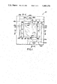
FIG. 1 is a plan view of an exemplary thin film bar resistor according to the invention;
FIG. 2 is a front elevation in cross section, not-to scale, taken as indicated by the arrows 2--2 in FIG. 1, of the FIG. 1 resistor; and
FIG. 3 is a side elevation in cross section, not-to scale, taken as indicated by the arrows 3--3 in FIG. 1, of the FIG. 1 resistor.
DETAILED DESCRIPTION OF EMBODIMENT
By way of introduction and as explained in "TFT," Section 7-1, a thin film on a substrate has a characteristic Rs which is known as "sheet" resistance, and which is equal to the specific resistivity in centimeter3 of the thin film material, divided by the thickness in centimeter of the film. The sheet resistance Rs can be considered as the resistance offered by one square centimeter of the film to passage of electric current from one side to the other of the square. The characteristic has however a greater significance. When the thin film is in the shape of a rectangular (square or oblong) bar having a length l and a width w, the lengthwise resistance of such bar evidently will be Rs ×l/w. The quantity (l/w) is dimensionless (i.e., is a pure number) so that, as a consequence, rectangular thin film regions of the same thinness and of the same material and having the same ratio of length l to width w will have the same lengthwise resistance for any size whatever of those regions. If the width w equals the length l so that the ratio (l/w) equals 1.0, each of those regions will be square in shape, from which it follows that the sheet resistance Rs of the thin film can be considered not only to be a characteristic of the thin film as such (whatever its size or shape) but also the actual lengthwise resistance of a square region of any size provided by the thin film. For this reason, the value of Rs is often expressed as "ohms per square."
An approach used in determining the lengthwise resistance of a rectangular thin film region is to, in effect, divide it into a number of squares of which the sides of each are equal to the width of the region, such width being sometimes referred to as the "line width." Numerically this is done by dividing the length l of the region by its width w to arrive at a number n which represents the number of such squares, and which may be either greater or less than 1.0 in dependence on whether l is greater or less than w. Thus, for purposes of determining its resistance, any such region can be considered as being so many "squares" or a specified fraction of a "square." For example, particular regions may be said to be "2.0 squares" or "0.5 square." In the case of a thin film bar resistor comprising several rectangular regions in series, the number of squares in each such region is computed, and the individual "square" values of those regions are then added to yield a figure which is the value in "squares" of the whole resistor.
It follows from the foregoing that a way of determining the resistance value of a thin film bar resistor is to multiply the sheet resistance value Rs of the included thin film by the value of n which expresses the sum of the number of squares contained in each of the constituent rectangular film regions of the resistor which contribute to its resistance. That is, the resistance of such resistor is the product of an electrical factor, Rs (sheet resistance), and of a geometric factor, n (number of squares), determined by the shape but not by the size of the resistor. Evidently, for any given thin film, the factor Rs will be fixed in value. Accordingly, the only way to reduce the resistance value of any size bar resistor made of such thin film is to reduce the geometric factor n characterizing the resistor or, in other words, the "square" value resulting from the geometry of the resistor. Such square value is reduced as later explained in the thin film bar resistor which is shown in the figures hereof, and which resistor will now be described.
Referring to FIGS. 1-3, the reference numeral 10 designates a thin film bar resistor which may be a discrete resistor but which is more likely to be (and is considered herein as being) a part of a larger thin film integrated circuit primarily provided by a pattern formed in a thin film 11 constituted in some places in the pattern of a single film layer and in other places in the pattern of a plurality of thin film layers. Resistor 10 includes an insulative substrate 12 which supports all of the thin film pattern of such circuit but which, for convenience, is shown (FIG. 1) as being broken away so that only the portion of substrate 12 allocable to resistor 10 illustrated. Substrate 12 is preferably a glazed or unglazed alumina substrate.
Substrate 12 supports thereon the elements of thin film 11 which are included in resistor 10. Among those elements are a pair of longitudinally-spaced, transversely-extending resistor terminals 15a, 15b comprising (a) a pair of transverse strip regions 16a, 16b (FIG. 2) of valve metal deposited directly on substrate 12 and providing the primary film layer of film 11, and (b) electrically conductive film layer strips 17a, 17b deposited on regions 16a, 16b and constituted of a metallic material of much lower resistance than the mentioned valve metal. That is, strips 17a, 17b render terminals 15a, 15b electrically conductive in the sense of offering insignificant resistance as compared to the portions of film 11 included in resistor 10 and not overlain by such conductive film layers.
Preferably, the mentioned valve metal is tantalum nitride, and it is to be understood that the term "tantalum nitride" as used herein includes in its meaning oxygen doped tantalum nitride which is frequently referred to as "tantalum oxynitride." If desired, however, the valve metal which provides the primary film layer of film 11 may be one of the other valve metals described in TFT, Section 5.4 and listed in TFT, FIG. 5-8. When the strip regions are 42 ohm per square tantalum nitride on an unglazed alumina substrate, they are about 900 Angstroms thick. The metallic material constituting the conductive film layer strips 17a, 17b is shown as being a homogenous layer, but in practice such strips are preferably multi-layer structures each comprising a titanium layer about 700 Angstroms thick on the tantalum nitride, a palladium layer about 2000 Angstroms thick on the titanium and a gold layer about 15,000 Angstroms thick on the palladium. Other examples of suitable conductive layer structures are given in TFT, Section 7.4.
Disposed between conductive resistor terminals 15a, 15b is a rectangular thin film resistance body 20 which is shown in FIG. 1 as being a square body with recesses for pattern registration errors. Body 20 is constituted before anodization of tantalum nitride about 900 Angstroms thick. The opposite longitudinal ends of body 20 are separated from terminals 15a, 15b by the guard margins 21a, 21b, the purpose of which is later explained. Such guard margins are occupied by transverse film layer strip regions 22a, 22b of unanodized tantalum nitride valve metal, about 900 Angstroms thick, which are integrally joined with body 20 and terminals 15a, to 15b electrically connect the former and latter together.
The terminals 15a, 15b have connected thereto a pair of conductive leads 25a, 25b of the same structure as such terminals in that leads 25a, 25b are constituted (FIG. 3) of underlying film layer regions 26a, 26b of tantalum nitride valve metal and of overlying conductive film layer strips 27a, 27b having the same composition as the strips 17 of the terminals 15a, 15b. Leads 25a, 25b continue on substrate 12 beyond the places where such substrate is shown broken away (FIG. 1) to connect the thin film bar resistor 10 to other parts of the thin film integrated circuit on such substrate. The leads 25a, 25b may be considered to be, structurally speaking, extension of the terminals 15a, 15b.
Returning to resistance body 20, in the manufacture of a thin film integrated circuit, it is a common practice to simultaneously trim the resistance of all the component resistors of such circuit to values preselected for such resistors. Such trimming is done by a process which increases the resistance of such resistors beyond their original resistance value. One such process is anodization which is, as described in TFT, Sections 5.4 and 7.3, accomplished by (a) masking the thin film circuit with a mask having windows registering with the resistance bodies of the resistors of the circuit, (b) introducing a liquid or semi-liquid electrolyte into these windows to make contact with these bodies, and (c) passing electric current through the electrolyte and through such bodies (connected as anodes) to produce an anodizing (i.e., oxidizing) of them. The anodizing progresses from the bodies' top surfaces downward to reduce the thickness of their remaining unanodized metal until the resistance of the resistors has been increased to the value desired therefor, the anodizing current being thereupon discontinued. The foregoing explanation of anodization is highly simplified, and for further details on that technique, reference is made to the Sections of TFT set out above.
FIG. 1 depicts the results on resistor 10 of anodization. As shown in FIGS. 2 and 3, resistance body 20 comprises a lower layer 30 of unanodized tantalum nitride and an upper layer 31 of anodized tantalum nitride which is substantially non-conducting. Layer 30 is about 450 Angstroms thick so as to have a lesser thickness than the adjacent strip regions 22 of unanodized metal of about 900 Angstroms thickness. The (FIG. 1) dash-dash line 32 represents the outline of the window used during anodization to contain the electrolyte and to limit the area covered thereby to approximately that of body 20. Since there may be some spread of the electrolyte in contact with the thin film beyond the area defined by window 32 and there may be errors that occur in the registration of the electrolyte mask, guard margins such as margins 22 must be provided to prevent the electrolyte from reaching one or both of the resistor terminals 15a, 15b or reaching adjacent conductive leads 25a, 25b. The reason why such happening must be avoided is that the contact of the electrolyte with those conductive terminals would produce a "short" by-passing resistance body 20, and that body accordingly would not become anodized in response to passage of the mentioned current. In addition, it is necessary to assure complete coverage of the resistor body by providing an electrolyte window slightly larger than the width of the resistor body to allow for error in mask registration.
As so far described, resistor 10 is known to the art.
Coming now to the improvement according to the invention and matters relating thereto, it is often desirable, as has been pointed out, to miniaturize thin film bar resistors such as resistor 10 in order to miniaturize as a whole the integrated thin film circuit in which such resistors are contained and, thereby, to effect cost and space savings and increase the speed of operation of the circuit. Also, it is desirable that the circuit be so designed that the resistances of all its resistors be trimmed proportionally during anodization, and the range of resistor values available to the circuit designer be as great as possible. From the foregoing it follows that for the greatest miniaturization of adjustable resistors using anodization techniques, the resistor body should be contained within the smallest anodization mask window possible with practical manufacturing methods. When using a semi-liquid electrolyte, the smallest size of the width and length that defines the window is the least of such size that surface tension forces characterizing the anodizing electrolyte will not prevent it from passing through the window and contacting the resistance body, and be such that when the mask containing the window is removed, the electrolyte will remain deposited on the resistance body 20. In practice the minimum length and width dimensions of the anodizing window evidently are the same and form a square area. It follows that the smallest length of the body of a bar resistor is equal to the smallest practical anodizing window, and the length between resistor terminals 15a, 15b is equal to the length of the window 32 plus the guard margins 22a, 22b. Similarly, the width of the anodizing window together with required guard margins determines the minimum distance between adjacent thin film elements such as conductive leads 25a, 25b which traverse the lengthwise direction of resistor 10. As previously mentioned, the guard margins are required to prevent the electrolyte from shorting to the adjacent conductors. When, however, the object is to have the minimum resistance possible of the resistor 10 that has been miniaturized, the minimum width dimension required of the window to permit it to pass the electrolyte through it determines the maximum width of the body of a bar resistor and therefore the minimum resistance value attainable for a resistor that has been miniaturized insofar as the techniques for manufacturing them will allow. And as previously mentioned, an allowance in the width of the bar resistor should be provided to assure complete coverage of the resistor body by the electrolyte. This results in a bar resistor width slightly smaller than the width of the electrolyte window by an amount necessary to allow for mask registration errors.
Thus the geometry of resistor 10 as so far described obtains for an anodized thin film bar resistor the minimum resistance heretofore thought possible for a resistor of such kind which has been miniaturized insofar as manufacturing techniques will permit. The geometric factor of such minimum resistance resistor has a value which, taking into account not only the square value for the anodized body 20 but also the square values of un-anodized strip regions 22, is about 1.4 square.
Coming now to the improvement according to the invention, conductive lead 25a is laid out on substrate 12 (FIG. 1) to provide thereon a first circuit path 40a disposed on the substrate to be outward of body 20 in a first of the two opposite directions aligned with the transverse or width dimension of body 20, such first transverse direction being the "upward" direction in FIG. 1. More particularly, circuit path 40a is spaced outward in that transverse direction from a side portion 45a of body 20 which is adjacent to terminal 15a and is on that one of the transversely opposite sides of body 20 which is nearest to such circuit path. As shown, circuit path 40a is the form of an "L" having (a) a conductive transverse arm 41a integrally joined with and extending outward in the first transverse direction from terminal 15a, and (b) a conductive longitudinal arm 42a extending from an angular junction 43a with arms 41a longitudinally past side portion 45a. With circuit path 40a having such "L" configuration and being so disposed in relation to side portion 45a, the result is that arms 41a, 42a and that side portion bound three sides of a rectangular area 50a defined on substrate 12 by those elements, such arms and side portion enclosing the rectangular area 50a by a three sided enclosure which is continuous from one end to the other of the enclosure except for a gap 44a occurring between the transverse arm 41a and the side portion 45a.
The description just given of the elements 40a-45a and 50a applies with equal force to their counterpart elements 40b-45b and 50b which are shown in FIG. 1 as being in the lower right hand corner of resistor 10, and which are preferably (but not necessarily) included as parts of the resistor along with elements 40a-45a and 50a. It is to be noted that circuit path 40b is spaced from body 20 in the second of the mentioned transverse directions, such second direction being downward in FIG. 1.
Returning to area 50a, occupying that area is a thin film region 55a (FIGS. 1 and 3) about 900 Angstroms thick of unanodized tantalum nitride valve metal deposited on substrate 12. Region 55a (FIG. 3) may conveniently be integrally joined with, and an extension of, guard margin strip region 22a, and region 55a is, in any event, integrally joined (FIG. 3) with (a) the unanodized tantalum nitride thin film layer 30 underlying the side portion 45a (FIG. 1) of body 20 and (b) the unanodized thin film tantalum nitride layer 26a (FIG. 3) underlying longitudinal arm 42a. Preferably region 55a is also integrally joined with the unanodized tantalum nitride thin film layer underlying transverse arm 41a to thereby be electrically connected with that conductive arm over its length.
Region 55a, 55b thus forms an electrical bridge extending between side portion 45a and a length of circuit path 40a to provide a current shunt for resistor 10 around its terminal 15a and its guard margin strip region 22a. The presence of that shunt eliminates a significant amount of the resistance of resistor 10 which is seen between its leads and is introduced in part into the resistor by the presence therein of its strip region 22a. Thus, the bridge region 55a is alone adopted to lower the geometric factor of the resistance of resistor 10 below 1.4 square.
Preferably, however, the resistance lowering effect of bridge region 55a is supplemented by providing the matching bridge region 55b which further lowers the resistance of resistor 10. While either of regions 55a, 55b may have any desired longitudinal dimension so long as that region provides a current shunt around its adjacent guard margin strip region, the resistance reducing effect of each of such regions becomes larger with increase in its longitudinal dimension.
With resistor 10 having the geometry shown in FIG. 1 so that each of the side regions 45a, 45b which bound the bridge regions 55a, 55b has a length only slightly less than one-half of the entire length of body 20, the geometric factor for the resistance of resistor 10 (as seen between its leads 25a, 25b is reduced from 1.4 square to 1.18 square or to about 84% of the value which such factor has when resistor 10 is conventional in its geometry. Resistors of the same form factor as shown in FIG. 1 but utilizing only one side termination extending 80% of the length have been produced that yielded 0.9 square. A practical value of approximately 0.6 square can be achieved by the extension of the side terminations on both sides of the resistor body shown in FIG. 1 for 80% of the entire lengths of such sides. Hence, the invention hereof permits a substantial lowering beyond that heretofore thought possible in the resistance of anodized thin film bar resistors which have been miniaturized as much as their manufacturing techniques permit, thus extending the lower range of values available to circuit designers.
As a detail of design of resistor, the length and width dimensions of its body 20 may each conveniently be 1500 microns with the other dimensions of such resistor being to scale in FIG. 1, such dimensions being not limitative of the invention.
The above-described embodiment being exemplary only, it will be appreciated that additions thereto, omissions therefrom and modifications thereof can be made without departing from the spirit of the invention, and that, accordingly, the invention is not to be considered as limited save as is consonant with the recitals of the following claims.

Claims (9)

What is claimed is:
1. The improvement in a thin film bar resistor comprising an insulative substrate and thin film elements thereon of which the latter comprise: first and second longitudinally-spaced, transversely-extending conductive resistor terminals, a rectangular resistance body between said terminals and spaced therefrom by guard margins, said body having lower and upper layers of a valve metal which are, respectively, unanodized and anodized, first and second strip regions of said unanodized metal deposited in said margins to connect said first and said second terminals with longitudinally opposite ends of said body, and first and second conductive leads connected to respectively, said first and second terminals; said improvement comprising: a first conductive circuit path provided by said first lead and disposed on said substrate to be spaced outward, in a first of the two transverse directions, from a first portion of said body which is adjacent to said first terminal and is on a first of the transversely opposite sides of said body, and a first supplemental thin film region of said unanodized metal deposited on said substrate in integrally joined relation with such portion and with a length of said path to form on said substrate a first electrical bridge extending between such portion and such length and providing a current shunt around said first terminal and said first strip region.
2. The improvement according to claim 1 in which said first circuit path is in the form of an "L" having a transverse arm integrally joined with and extending outward in said first transverse direction from said first terminal and also, a longitudinal arm extending from its angular junction with said transverse arm longitudinally past said first side portion of said body so that such portion and arms bound three sides of a substantially rectangular area on said substrate, and in which said supplemental thin film region occupies said area to be integrally joined with said first body portion and with both of said arms of said first circuit path.
3. The improvement according to claim 1 in which said rectangular resistance body is a square body.
4. The improvement according to claim 1 in which said valve metal is tantalum nitride.
5. The improvement according to claim 1 in which said first supplemental thin film region of unanodized valve metal is integral with and an extension of said first strip region of unanodized valve metal.
6. The improvement according to claim 1 in which the thickness of metal in said first strip region and in said first supplemental thin film region is greater than the thickness of said lower layer of the resistance body.
7. The improvement according to claim 1 in which the length of said first side portion of said body is less than the entire length of said body and in which said electrical bridge is integral with such side portion over the length thereof.
8. The improvement according to claim 1 further comprising: a second conductive current path provided by said second lead to be spaced outward on said substrate in the second transverse direction from a second portion of said body which is adjacent to said second terminal and is on the second of the transversely opposite sides of said body, and a second supplemental thin film region of said unanodized metal deposited on said substrate between said second path and second side portion in integrally joined relation with such portion and with a length of said second path to form on said substrate a second electrical bridge extending between such portion and length and providing a current shunt around said second terminal and said second strip region.
9. The improvement in a thin film bar resistor comprising an insulative substrate and thin film elements thereon of which the latter comprise: first and second longitudinally-spaced, transversely-extending resistor terminals, a rectangular resistance body between said terminals and spaced therefrom by guard margins, said body having lower and upper layers of respectively, unanodized tantalum nitride and anodized tantalum nitride, first and second strip regions of unanodized tantalum nitride deposited in said margins to connect said first and second terminals with longitudinally opposite ends of said body, and first and second conductive leads connected to, respectively, said first and second terminals; said improvement comprising, first and second circuit paths provided on said substrate by said first and second leads and each in the form of an "L" having a transverse arm and a longitudinal arm, the respective transverse arms of said first and second paths being integrally joined with respectively, said first and second terminals and extending transversely outward thereof in first and second, respectively, of the opposite transverse directions on said substrate, and the respective longitudinal arms of said first and second paths extending in transversely spaced relation from, and longitudinally past, first and second portions of said body which are on transversely opposite sides thereof, and are adjacent to, respectively, said first and second terminals, said first and second side portions of said body and said first and second paths being cooperable to provide bounds on three sides for first and second rectangular areas defined on said substrate and each bounded by one of such side portions and the arms of the current path adjacent that portion, and first and second supplemental thin film regions of unanodized tantalum nitride each occupying a respective one of said first and second areas to be integrally joined with the body's side portion bounding that area and, also, with the said transverse and longitudinal arms which bound that area so as to form on said substrate an electrical bridge extending between such portion and such arms and providing a current shunt around the adjacent terminal and the adjacent strip region, each of said supplemental regions being also integrally joined with and an extension of the adjacent strip region of unanodized tantalum nitride.
US06/584,966 1984-02-29 1984-02-29 Thin film bar resistor Expired - Fee Related US4485370A (en)

Priority Applications (1)

Application Number Priority Date Filing Date Title
US06/584,966 US4485370A (en) 1984-02-29 1984-02-29 Thin film bar resistor

Applications Claiming Priority (1)

Application Number Priority Date Filing Date Title
US06/584,966 US4485370A (en) 1984-02-29 1984-02-29 Thin film bar resistor

Publications (1)

Publication Number Publication Date
US4485370A true US4485370A (en) 1984-11-27

Family

ID=24339485

Family Applications (1)

Application Number Title Priority Date Filing Date
US06/584,966 Expired - Fee Related US4485370A (en) 1984-02-29 1984-02-29 Thin film bar resistor

Country Status (1)

Country Link
US (1) US4485370A (en)

Cited By (7)

* Cited by examiner, † Cited by third party
Publication number Priority date Publication date Assignee Title
US4758816A (en) * 1984-08-11 1988-07-19 Vdo Adolf Schindling Ag Electrical resistor
US4788524A (en) * 1987-08-27 1988-11-29 Gte Communication Systems Corporation Thick film material system
US5521357A (en) * 1992-11-17 1996-05-28 Heaters Engineering, Inc. Heating device for a volatile material with resistive film formed on a substrate and overmolded body
US5559543A (en) * 1989-03-01 1996-09-24 Canon Kabushiki Kaisha Method of making uniformly printing ink jet recording head
US20020197811A1 (en) * 2001-06-20 2002-12-26 Alps Electric Co., Ltd. Thin-film resistor and method for manufacturing the same
US20040140529A1 (en) * 2000-11-14 2004-07-22 Ballantine Arne W. Increasing an electrical resistance of a resistor by oxidation or nitridization
US6996837B1 (en) * 1999-08-27 2006-02-07 Pioneer Corporation Terminal equipment for cable television

Citations (5)

* Cited by examiner, † Cited by third party
Publication number Priority date Publication date Assignee Title
US3405382A (en) * 1965-09-13 1968-10-08 Beckman Instruments Inc Terminal and tap connections for resistance element
US3460026A (en) * 1966-12-16 1969-08-05 Bell Telephone Labor Inc N-port monolithic thin film distributed resistance network
US3473146A (en) * 1967-10-10 1969-10-14 Trw Inc Electrical resistor having low resistance values
GB1367983A (en) * 1972-05-25 1974-09-25 Standard Telephones Cables Ltd Electrical circuit elements
US4079349A (en) * 1976-09-29 1978-03-14 Corning Glass Works Low TCR resistor

Patent Citations (5)

* Cited by examiner, † Cited by third party
Publication number Priority date Publication date Assignee Title
US3405382A (en) * 1965-09-13 1968-10-08 Beckman Instruments Inc Terminal and tap connections for resistance element
US3460026A (en) * 1966-12-16 1969-08-05 Bell Telephone Labor Inc N-port monolithic thin film distributed resistance network
US3473146A (en) * 1967-10-10 1969-10-14 Trw Inc Electrical resistor having low resistance values
GB1367983A (en) * 1972-05-25 1974-09-25 Standard Telephones Cables Ltd Electrical circuit elements
US4079349A (en) * 1976-09-29 1978-03-14 Corning Glass Works Low TCR resistor

Non-Patent Citations (1)

* Cited by examiner, † Cited by third party
Title
Thin Film Technology, Berry et al., D. Van Nostrand and Co., 1968. *

Cited By (15)

* Cited by examiner, † Cited by third party
Publication number Priority date Publication date Assignee Title
US4758816A (en) * 1984-08-11 1988-07-19 Vdo Adolf Schindling Ag Electrical resistor
US4788524A (en) * 1987-08-27 1988-11-29 Gte Communication Systems Corporation Thick film material system
US5559543A (en) * 1989-03-01 1996-09-24 Canon Kabushiki Kaisha Method of making uniformly printing ink jet recording head
US5521357A (en) * 1992-11-17 1996-05-28 Heaters Engineering, Inc. Heating device for a volatile material with resistive film formed on a substrate and overmolded body
US6996837B1 (en) * 1999-08-27 2006-02-07 Pioneer Corporation Terminal equipment for cable television
US7351639B2 (en) * 2000-11-14 2008-04-01 International Business Machines Corporation Increasing an electrical resistance of a resistor by oxidation or nitridization
US20040140529A1 (en) * 2000-11-14 2004-07-22 Ballantine Arne W. Increasing an electrical resistance of a resistor by oxidation or nitridization
US20070267286A1 (en) * 2000-11-14 2007-11-22 Ballantine Arne W Increasing an electrical resistance of a resistor by oxidation or nitridization
US20080102543A1 (en) * 2000-11-14 2008-05-01 Ballantine Arne W Increasing an electrical resistance of a resistor by oxidation
US7456074B2 (en) 2000-11-14 2008-11-25 International Business Machines Corporation Increasing an electrical resistance of a resistor by nitridization
US20080314754A1 (en) * 2000-11-14 2008-12-25 Ballantine Arne W Increasing an electrical resistance of a resistor by nitridization
US20090011526A1 (en) * 2000-11-14 2009-01-08 Ballantine Arne W Increasing an electrical resistance of a resistor by nitridization
US8440522B2 (en) 2000-11-14 2013-05-14 International Business Machines Corporation Increasing an electrical resistance of a resistor by oxidation
US6777778B2 (en) * 2001-06-20 2004-08-17 Alps Electric Co., Ltd. Thin-film resistor and method for manufacturing the same
US20020197811A1 (en) * 2001-06-20 2002-12-26 Alps Electric Co., Ltd. Thin-film resistor and method for manufacturing the same

Similar Documents

Publication Publication Date Title
US4470096A (en) Multilayer, fully-trimmable, film-type capacitor and method of adjustment
US3862017A (en) Method for producing a thin film passive circuit element
US6223423B1 (en) Multilayer conductive polymer positive temperature coefficient device
US5075665A (en) Laminated varistor
US6115264A (en) Multilayer high frequency electronic parts
US6005474A (en) Chip network resistor and method for manufacturing same
US3699011A (en) Method of producing thin film integrated circuits
US3988824A (en) Method for manufacturing thin film circuits
KR940006179A (en) Semiconductor device and manufacturing method
US4485370A (en) Thin film bar resistor
US5757076A (en) Chip type electronic component
US4528546A (en) High power thick film
IL45045A (en) Thin-film electrical circuit
JP3756612B2 (en) Structure of chip resistor and manufacturing method thereof
KR920005985B1 (en) Post-termination process for thick-film resistors of printed circuit boards
US5227323A (en) Method of manufacturing capacitor elements in an integrated circuit having a compound semiconductor substrate
US5274352A (en) Thick film resistive element, thick film printed circuit board and thick film hybrid integrated circuit device and their production methods
US5257005A (en) Small value precision integrated circuit resistors
EP0072644B1 (en) Semiconductor chip carrier
KR100206621B1 (en) Chip type thick film capacitor and method of making the same
Worobey et al. Tantalum thin-film RC circuit technology for a universal active filter
JPS617649A (en) Method of forming circuit board
JP2707717B2 (en) Hybrid integrated circuit
JPH0247862A (en) Semiconductor integrated circuit device
JP3766492B2 (en) Structure of chip resistor and manufacturing method thereof

Legal Events

Date Code Title Description
AS Assignment

Owner name: AMERICAN TELEPHONE AND TELEGRAPH COMPANY 550 MADIS

Free format text: ASSIGNMENT OF ASSIGNORS INTEREST.;ASSIGNOR:POISEL, C. EDWARD;REEL/FRAME:004237/0358

Effective date: 19840221

AS Assignment

Owner name: NIPPON LIGHT METAL COMPANY LIMITED, 3-5, 7-CHOME,

Free format text: ASSIGNMENT OF ASSIGNORS INTEREST.;ASSIGNORS:YOSHIDA, KOICHI;HIRAYAMA, YOSHIO;OKA, YASUO;AND OTHERS;REEL/FRAME:004394/0477

Effective date: 19840220

FEPP Fee payment procedure

Free format text: PAYOR NUMBER ASSIGNED (ORIGINAL EVENT CODE: ASPN); ENTITY STATUS OF PATENT OWNER: LARGE ENTITY

FPAY Fee payment

Year of fee payment: 4

REMI Maintenance fee reminder mailed
LAPS Lapse for failure to pay maintenance fees
FP Lapsed due to failure to pay maintenance fee

Effective date: 19921129

STCH Information on status: patent discontinuation

Free format text: PATENT EXPIRED DUE TO NONPAYMENT OF MAINTENANCE FEES UNDER 37 CFR 1.362