US4327129A - Method of making laser beam optical decoupling element for an astable laser resonator - Google Patents
Method of making laser beam optical decoupling element for an astable laser resonator Download PDFInfo
- Publication number
- US4327129A US4327129A US06/109,925 US10992580A US4327129A US 4327129 A US4327129 A US 4327129A US 10992580 A US10992580 A US 10992580A US 4327129 A US4327129 A US 4327129A
- Authority
- US
- United States
- Prior art keywords
- substrate
- laser
- mask
- astable
- boundary
- Prior art date
- Legal status (The legal status is an assumption and is not a legal conclusion. Google has not performed a legal analysis and makes no representation as to the accuracy of the status listed.)
- Expired - Lifetime
Links
- 230000003287 optical effect Effects 0.000 title claims abstract description 24
- 238000004519 manufacturing process Methods 0.000 title claims abstract description 11
- 239000000758 substrate Substances 0.000 claims abstract description 36
- 230000005855 radiation Effects 0.000 claims abstract description 18
- 239000000463 material Substances 0.000 claims abstract description 16
- 238000005498 polishing Methods 0.000 claims description 5
- 238000000227 grinding Methods 0.000 claims description 4
- 238000000151 deposition Methods 0.000 claims description 3
- 238000007740 vapor deposition Methods 0.000 abstract description 4
- 239000011248 coating agent Substances 0.000 abstract description 3
- 238000000576 coating method Methods 0.000 abstract description 3
- 230000000873 masking effect Effects 0.000 description 10
- 238000000034 method Methods 0.000 description 8
- 230000008901 benefit Effects 0.000 description 6
- VYPSYNLAJGMNEJ-UHFFFAOYSA-N Silicium dioxide Chemical compound O=[Si]=O VYPSYNLAJGMNEJ-UHFFFAOYSA-N 0.000 description 4
- GWEVSGVZZGPLCZ-UHFFFAOYSA-N Titan oxide Chemical compound O=[Ti]=O GWEVSGVZZGPLCZ-UHFFFAOYSA-N 0.000 description 4
- 238000009760 electrical discharge machining Methods 0.000 description 4
- WCUXLLCKKVVCTQ-UHFFFAOYSA-M Potassium chloride Chemical compound [Cl-].[K+] WCUXLLCKKVVCTQ-UHFFFAOYSA-M 0.000 description 3
- PFNQVRZLDWYSCW-UHFFFAOYSA-N (fluoren-9-ylideneamino) n-naphthalen-1-ylcarbamate Chemical compound C12=CC=CC=C2C2=CC=CC=C2C1=NOC(=O)NC1=CC=CC2=CC=CC=C12 PFNQVRZLDWYSCW-UHFFFAOYSA-N 0.000 description 2
- PXHVJJICTQNCMI-UHFFFAOYSA-N Nickel Chemical compound [Ni] PXHVJJICTQNCMI-UHFFFAOYSA-N 0.000 description 2
- MCMNRKCIXSYSNV-UHFFFAOYSA-N Zirconium dioxide Chemical compound O=[Zr]=O MCMNRKCIXSYSNV-UHFFFAOYSA-N 0.000 description 2
- BYJADUSHMADYRW-UHFFFAOYSA-L cadmium(2+);sulfite Chemical compound [Cd+2].[O-]S([O-])=O BYJADUSHMADYRW-UHFFFAOYSA-L 0.000 description 2
- GKMPTXZNGKKTDU-UHFFFAOYSA-L cadmium(2+);tellurite Chemical compound [Cd+2].[O-][Te]([O-])=O GKMPTXZNGKKTDU-UHFFFAOYSA-L 0.000 description 2
- 230000003292 diminished effect Effects 0.000 description 2
- 229910052751 metal Inorganic materials 0.000 description 2
- 239000002184 metal Substances 0.000 description 2
- 230000004048 modification Effects 0.000 description 2
- 238000012986 modification Methods 0.000 description 2
- 239000012071 phase Substances 0.000 description 2
- 239000000377 silicon dioxide Substances 0.000 description 2
- 239000000126 substance Substances 0.000 description 2
- 230000009466 transformation Effects 0.000 description 2
- 238000005019 vapor deposition process Methods 0.000 description 2
- 229910052984 zinc sulfide Inorganic materials 0.000 description 2
- 229910018404 Al2 O3 Inorganic materials 0.000 description 1
- VYZAMTAEIAYCRO-UHFFFAOYSA-N Chromium Chemical compound [Cr] VYZAMTAEIAYCRO-UHFFFAOYSA-N 0.000 description 1
- RYGMFSIKBFXOCR-UHFFFAOYSA-N Copper Chemical compound [Cu] RYGMFSIKBFXOCR-UHFFFAOYSA-N 0.000 description 1
- GYHNNYVSQQEPJS-UHFFFAOYSA-N Gallium Chemical compound [Ga] GYHNNYVSQQEPJS-UHFFFAOYSA-N 0.000 description 1
- BQCADISMDOOEFD-UHFFFAOYSA-N Silver Chemical compound [Ag] BQCADISMDOOEFD-UHFFFAOYSA-N 0.000 description 1
- 229910004366 ThF4 Inorganic materials 0.000 description 1
- 239000005083 Zinc sulfide Substances 0.000 description 1
- 238000010521 absorption reaction Methods 0.000 description 1
- 239000000853 adhesive Substances 0.000 description 1
- 230000001070 adhesive effect Effects 0.000 description 1
- 229910052782 aluminium Inorganic materials 0.000 description 1
- XAGFODPZIPBFFR-UHFFFAOYSA-N aluminium Chemical compound [Al] XAGFODPZIPBFFR-UHFFFAOYSA-N 0.000 description 1
- AQLMHYSWFMLWBS-UHFFFAOYSA-N arsenite(1-) Chemical compound O[As](O)[O-] AQLMHYSWFMLWBS-UHFFFAOYSA-N 0.000 description 1
- 229910052804 chromium Inorganic materials 0.000 description 1
- 239000011651 chromium Substances 0.000 description 1
- 229910052681 coesite Inorganic materials 0.000 description 1
- 229910052802 copper Inorganic materials 0.000 description 1
- 239000010949 copper Substances 0.000 description 1
- 229910052906 cristobalite Inorganic materials 0.000 description 1
- 230000000694 effects Effects 0.000 description 1
- 238000005530 etching Methods 0.000 description 1
- -1 for example Substances 0.000 description 1
- 229910052733 gallium Inorganic materials 0.000 description 1
- 229910052732 germanium Inorganic materials 0.000 description 1
- GNPVGFCGXDBREM-UHFFFAOYSA-N germanium atom Chemical compound [Ge] GNPVGFCGXDBREM-UHFFFAOYSA-N 0.000 description 1
- PCHJSUWPFVWCPO-UHFFFAOYSA-N gold Chemical compound [Au] PCHJSUWPFVWCPO-UHFFFAOYSA-N 0.000 description 1
- 229910052737 gold Inorganic materials 0.000 description 1
- 239000010931 gold Substances 0.000 description 1
- 238000003801 milling Methods 0.000 description 1
- 229910052759 nickel Inorganic materials 0.000 description 1
- TWNQGVIAIRXVLR-UHFFFAOYSA-N oxo(oxoalumanyloxy)alumane Chemical compound O=[Al]O[Al]=O TWNQGVIAIRXVLR-UHFFFAOYSA-N 0.000 description 1
- RVTZCBVAJQQJTK-UHFFFAOYSA-N oxygen(2-);zirconium(4+) Chemical compound [O-2].[O-2].[Zr+4] RVTZCBVAJQQJTK-UHFFFAOYSA-N 0.000 description 1
- 239000001103 potassium chloride Substances 0.000 description 1
- 235000011164 potassium chloride Nutrition 0.000 description 1
- 238000007493 shaping process Methods 0.000 description 1
- 235000012239 silicon dioxide Nutrition 0.000 description 1
- 229910052709 silver Inorganic materials 0.000 description 1
- 239000004332 silver Substances 0.000 description 1
- 229910052682 stishovite Inorganic materials 0.000 description 1
- 229910019655 synthetic inorganic crystalline material Inorganic materials 0.000 description 1
- 239000010409 thin film Substances 0.000 description 1
- MZQZQKZKTGRQCG-UHFFFAOYSA-J thorium tetrafluoride Chemical compound F[Th](F)(F)F MZQZQKZKTGRQCG-UHFFFAOYSA-J 0.000 description 1
- 239000004408 titanium dioxide Substances 0.000 description 1
- 229910052905 tridymite Inorganic materials 0.000 description 1
- 238000001771 vacuum deposition Methods 0.000 description 1
- 239000012808 vapor phase Substances 0.000 description 1
- 229910019901 yttrium aluminum garnet Inorganic materials 0.000 description 1
- DRDVZXDWVBGGMH-UHFFFAOYSA-N zinc;sulfide Chemical compound [S-2].[Zn+2] DRDVZXDWVBGGMH-UHFFFAOYSA-N 0.000 description 1
- 229910001928 zirconium oxide Inorganic materials 0.000 description 1
Images
Classifications
-
- H—ELECTRICITY
- H01—ELECTRIC ELEMENTS
- H01S—DEVICES USING THE PROCESS OF LIGHT AMPLIFICATION BY STIMULATED EMISSION OF RADIATION [LASER] TO AMPLIFY OR GENERATE LIGHT; DEVICES USING STIMULATED EMISSION OF ELECTROMAGNETIC RADIATION IN WAVE RANGES OTHER THAN OPTICAL
- H01S3/00—Lasers, i.e. devices using stimulated emission of electromagnetic radiation in the infrared, visible or ultraviolet wave range
- H01S3/05—Construction or shape of optical resonators; Accommodation of active medium therein; Shape of active medium
- H01S3/08—Construction or shape of optical resonators or components thereof
- H01S3/08081—Unstable resonators
-
- H—ELECTRICITY
- H01—ELECTRIC ELEMENTS
- H01S—DEVICES USING THE PROCESS OF LIGHT AMPLIFICATION BY STIMULATED EMISSION OF RADIATION [LASER] TO AMPLIFY OR GENERATE LIGHT; DEVICES USING STIMULATED EMISSION OF ELECTROMAGNETIC RADIATION IN WAVE RANGES OTHER THAN OPTICAL
- H01S3/00—Lasers, i.e. devices using stimulated emission of electromagnetic radiation in the infrared, visible or ultraviolet wave range
- H01S3/05—Construction or shape of optical resonators; Accommodation of active medium therein; Shape of active medium
- H01S3/08—Construction or shape of optical resonators or components thereof
- H01S3/08059—Constructional details of the reflector, e.g. shape
- H01S3/08063—Graded reflectivity, e.g. variable reflectivity mirror
Definitions
- the present invention relates to an optical element for an astable laser resonator which element may be employed as an output reflector and/or as a lens.
- the output reflectors for such resonators had either a circular or a rectangular, more specifically a square cross section or configuration.
- theoretical considerations as, for example, described in IEE "Journal of Quantum Electronics", Volume QE-10, No. 3, pages 346 to 355, March 1974 have shown that such uniform or regular boundaries cause constructive interferences at the location of the virtual focus of the resonator.
- Such constructive interferences in turn cause non-homogeneous phase and amplitude profiles of the internal radiation field.
- Such interferences also increase the divergence of the output laser beam and they decrease the mode discrimination ratio which is a measure or indication for the operation of the laser, more specifically, whether the laser operates at all and how easily it operates in the phase mode of operation.
- the beam decoupling has been accomplished by means of a metal output reflector having a given radius of curvature which is determined by the resonator geometry and which has lateral dimensions smaller than the lateral dimensions of the radiation field in the resonator.
- These reflectors are convex full mirrors where the resonator is of the confocal type which is normally preferred.
- the beam decoupled from the laser corresponds to that proportion of the radiation field which extends outside the boundary of the reflector mirror.
- auxiliary metallic mirror which is arranged in a slanted manner in the beam path ahead of the convex output reflector.
- This auxiliary mirror is normally a plain mirror provided with an aperture located concentrically in the beam path and having a smaller diameter than the diameter of the convex mirror or output reflector.
- This prior art arrangement corresponds, relative to the resonator geometry, precisely to the output reflector described above having the same diameter as the central opening of the plain mirror except that the output beam does not extend in the direction of the resonator axis but rather perpendicularly thereto.
- an optical element which is capable of simultaneously performing several functions, namely, as an output reflector and as a lens in an astable laser;
- optical element which may also function as an exit window for an astable laser resonator.
- an optical element for an astable laser resonator having a given resonator configuration comprising a laser beam optical decoupling element for a astable laser resonator having a given configuration, comprising a substrate transparent for the respective laser radiation and having ground and polished front and rear surfaces, said surfaces being flat or curved, said substrate further having on one of said surfaces a central area and an outer area as well as a boundary of a predetermined shape separating said areas, and a highly reflective layer covering one of said areas, whereas the other of said areas remains transparent for said laser radiation, said boundary shape being computed to obtain a diffraction limited divergence of the laser beam.
- a highly reflective layer relative to the laser radiation covers one of said areas whereas the other area remains transparent for the laser radiation whereby a diffraction limited divergence is obtained.
- an anti-reflection layer may be applied to one or both surfaces of the substrate prior to the application of the reflective layer.
- these layers may be applied by preparing a substrate of a material which is transparent to the respective laser radiation, said preparing including grinding and polishing the front and rear surfaces of said substrate, preparing a mask to have a mathematically computed boundary configuration such that said optical element provides a diffraction limited divergence, securing said mask to one surface of said substrate, whereby said boundary configuration separates a central area from an outer area on said substrate surface, and vapor depositing a highly reflective layer on said substrate, whereby said highly reflective layer covers one of said areas.
- the highly reflective layer may be applied to the central zone or to the outer zone surrounding the central zone.
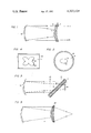
- FIG. 1 is a sectional view through one embodiment of an optical element according to the invention.
- FIG. 2 is a plan view of the embodiment according to FIG. 1;
- FIG. 3 is a sectional view through a second embodiment according to the invention.
- FIG. 4 is a plan view of the embodiment according to FIG. 3 and showing a different boundary configuration as compared to FIG. 2;
- FIG. 5 is a view similar to that of FIG. 1 but showing a beam converging rear surface.
- FIG. 1 shows a sectional view of a substrate 10 which is made of a material transparent to the respective laser radiation.
- a suitable material for the substrate 10 is, for example, germanium which could be used for a CO 2 laser.
- other materials could also be employed as a substrate, for example, potassium chloride (KCL), gallium arsenite (GaAs), cadmium tellurite (CdTe), zinc selenide (ZnSe), cadmium sulfite (CdS) and similar materials are suitable.
- KCL potassium chloride
- GaAs gallium arsenite
- CdTe cadmium tellurite
- ZnSe zinc selenide
- CdS cadmium sulfite
- the substrate 10 in the embodiment of FIG. 1 has a curvature which is determined by the respective curvature of the other laser components such as the reflector 14 in this particular or special astable resonator.
- FIG. 1 illustrates a positive confocal resonator in which the spacing between the reflectors would be about 1 meter.
- the radius R 1 of the reflector or mirror 14 could be +7 meters and the radius R 2 of curvature of the output reflector 20 with the substrate 10 would be -5 meters.
- the substrate 10 is provided with an optical surface on both sides, for example, by grinding and polishing. The precision of an optical surface in the present instance might correspond to ⁇ /20, ⁇ being the wave length of the radiation.
- the so prepared surfaces of the substrate 10 may, if desired, be coated with an anti-reflection layer 11.
- an anti-reflection layer may, for example, be produced by a vapor deposition of suitable materials and to a thickness of 0.19 to 1.5 microns where the dielectric anti-reflection layers are made of silicon dioxide SiO 2 , titanium dioxide TiO 2 , zirconium oxide ZrO 2 , or aluminum oxide Al 2 O 3 .
- the layer 11 will be somewhat thicker, for example, in the range of 1.5 to 16 microns where the material is thorium fluoride ThF 4 or zinc sulfide ZnS.
- the substrate prepared as described above, is provided with a highly reflective layer 12 which in the embodiment of FIGS. 1 and 2 is centrally located and separated from the outer area by a boundary 13, for example, of elliptical shape as shown in FIG. 2.
- the highly reflective layer may also be deposited from a vapor phase of a suitable material, such as gold, silver, nickel, chromium, copper, aluminum and similar suitable materials.
- the material combination for the highly reflective area and for the anti-reflection layer and the substrate should be selected so that the reflecting area has a high reflection coefficient for the respective laser radiation whereas the transparent portion should have a reflection coefficient as small as possible.
- the transparent portion should absorb the laser radiation as little as possible.
- the highly reflecting layer may be produced according to the present method by masking the areas which are not to be coated in the vapor deposition process.
- the masking may be glued to the surface of the substrate where the masking has been produced by mechanical means, for example, stamping.
- the masking may also be produced by photo-chemical means or by photographic means, as are well known in the art.
- the masking materials may be metallic or non-metallic and it may correspond in its boundary configuration to a "negative" of the boundary 13 separating the highly reflective layer 12 from the remaining area of the element.
- the substrate with the masking secured thereto, for example, by a suitable adhesive is then placed into a suitable apparatus for vapor deposition of the highly reflective layer.
- the central area 12 is highly reflective and the reflector itself has the curvature R2 which is determined by the geometry of the resonator.
- the contour 13 corresponds to the shape of the mask used as described.
- the area 11 surrounding the highly reflective area 12 remains transparent for the laser radiation and the substrate may have any desired radius of curvature in this transparent area.
- the dimensions of the substrate in the lateral direction are selected so that the entire output or decoupled beam is covered. This has the advantage that the so-called exit window for the laser beam, which has been required heretofore, may be obviated.
- the decoupled laser beam is subjected to a lens effect when it passes through the substrate.
- a collimated beam or a convergent beam or a divergent laser beam By providing the rear surface of the substrate with a suitable shape, it is possible to provide a collimated beam or a convergent beam or a divergent laser beam. This has the advantage that in certain instances of use an additional lens will not be required as heretofore.
- a collimated beam can be produced if the two surfaces of the output reflector have substantially the same radius of curvature.
- a convergent or a divergent decoupled beam may be produced in accordance with optical lens requirements by respectively shaping the substrate.
- This feature of the invention has the advantage that the dimensions and shape, in other words, the geometry of the resonator may now be more freely selected. Further, a collimated beam may now be produced not only by a confocal resonator, but also by a symmetric or an asymmetric resonator provided that the rear surface
- the highly reflective material or layer 12 surrounds the transparent area 11 which may be covered with an anti-reflection material and the boundary 13 between the two areas has a rosette shape as best seen in FIG. 4.
- the output or decoupled laser beam 15 exits the resonator as shown.
- the direction of the output beam 15 is at right angles to the direction of the resonator beam.
- the substrate with the respective coating forms a highly reflective mirror whereby the central region inside the boundary 13 remains transparent for the laser beam.
- the mask has the shape of the rosette shown.
- the configuration of the boundary 13 is not subject to any manufacturing limitations because the masking employed in the vapor deposition process can be produced in any desirable shape with conventional means at reasonable costs. Thus, it is possible to realize the above mentioned theoretical advantages.
- the present element may function for two purposes, namely, as a decoupling reflector and as a lens whereby it is possible to dimension and select the resonator parameters accordingly and to obviate an additional lens.
- the embodiment of FIGS. 1 and 2 can also be used as an exit window.
- Nd neodium; YAG-yttrium-aluminum-garnet
- the present teaching may be employed in connection with high output gas dynamic lasers, for example a gas dynamic CO 2 laser provided that substrate materials are employed having a low absorption for the laser radiation and a high heat conductivity.
- FIG. 5 shows a sectional view similar to that of FIG. 1 but with the modification that the rear surface of the substrate has a shape such that the output laser beam converges.
Landscapes
- Physics & Mathematics (AREA)
- Electromagnetism (AREA)
- Engineering & Computer Science (AREA)
- Plasma & Fusion (AREA)
- Optics & Photonics (AREA)
- Lasers (AREA)
- Optical Elements Other Than Lenses (AREA)
Applications Claiming Priority (2)
| Application Number | Priority Date | Filing Date | Title |
|---|---|---|---|
| DE2449123 | 1974-10-16 | ||
| DE2449123A DE2449123C3 (de) | 1974-10-16 | 1974-10-16 | Auskoppelspiegel für astabile Laserresonatoren |
Related Parent Applications (1)
| Application Number | Title | Priority Date | Filing Date |
|---|---|---|---|
| US05912388 Continuation | 1978-06-05 |
Publications (1)
| Publication Number | Publication Date |
|---|---|
| US4327129A true US4327129A (en) | 1982-04-27 |
Family
ID=5928376
Family Applications (1)
| Application Number | Title | Priority Date | Filing Date |
|---|---|---|---|
| US06/109,925 Expired - Lifetime US4327129A (en) | 1974-10-16 | 1980-01-07 | Method of making laser beam optical decoupling element for an astable laser resonator |
Country Status (3)
| Country | Link |
|---|---|
| US (1) | US4327129A (OSRAM) |
| DE (1) | DE2449123C3 (OSRAM) |
| FR (1) | FR2288404A1 (OSRAM) |
Cited By (11)
| Publication number | Priority date | Publication date | Assignee | Title |
|---|---|---|---|---|
| US4749255A (en) * | 1985-12-09 | 1988-06-07 | American Telephone And Telegraph Company, At&T Bell Laboratories | Coating for optical devices |
| US4903271A (en) * | 1987-06-03 | 1990-02-20 | Mitsubishi Denki Kabushiki Kaisha | Laser apparatus |
| US4918704A (en) * | 1989-01-10 | 1990-04-17 | Quantel International, Inc. | Q-switched solid state pulsed laser with injection seeding and a gaussian output coupling mirror |
| US4937424A (en) * | 1987-07-20 | 1990-06-26 | Mitsubishi Denki Kabushiki Kaisha | Laser machining apparatus |
| US4942588A (en) * | 1985-11-20 | 1990-07-17 | Mitsubishi Denki Kabushiki Kaisha | Laser device |
| US5058123A (en) * | 1986-12-08 | 1991-10-15 | Mitsubishi Denki K.K. | Laser apparatus |
| US5708675A (en) * | 1995-02-08 | 1998-01-13 | Litton Systems, Inc. | Laser apparatus |
| US6656373B1 (en) * | 1999-07-09 | 2003-12-02 | Wavefront Sciences, Inc. | Apodized micro-lenses for Hartmann wavefront sensing and method for fabricating desired profiles |
| US20060013997A1 (en) * | 2004-07-15 | 2006-01-19 | Schott Ag | Coated substrate with a curved surface, and a method for production of a coated substrate such as this |
| US20200251874A1 (en) * | 2019-01-31 | 2020-08-06 | L3Harris Technologies, Inc. | Continuous wave end-pumped laser |
| EP3793044A1 (en) * | 2019-09-12 | 2021-03-17 | Kern Technologies, LLC | Output coupling from unstable laser resonators |
Families Citing this family (6)
| Publication number | Priority date | Publication date | Assignee | Title |
|---|---|---|---|---|
| US4429400A (en) * | 1980-11-12 | 1984-01-31 | United Kingdom Atomic Energy Authority | Lasers |
| DE3133142C2 (de) * | 1981-06-29 | 1985-06-13 | Messerschmitt-Bölkow-Blohm GmbH, 8000 München | Stabiler optischer Resonator bei Lasern |
| DE3125544C2 (de) * | 1981-06-29 | 1984-03-08 | Messerschmitt-Bölkow-Blohm GmbH, 8000 München | Stabiler optischer Resonator bei Lasern |
| DE3725573C2 (de) * | 1987-08-01 | 1994-08-18 | Deutsche Aerospace | Optischer Resonator |
| DE3728129A1 (de) * | 1987-08-22 | 1988-03-31 | Norman Dipl Phys Hodgson | Laseranordnung aus einem astabilen optischen resonator und einer zusaetzlichen teilreflektierenden flaeche |
| DE3913188C2 (de) * | 1988-04-22 | 1993-11-04 | Fraunhofer Ges Forschung | Laserresonator |
Citations (1)
| Publication number | Priority date | Publication date | Assignee | Title |
|---|---|---|---|---|
| US3846165A (en) * | 1972-08-21 | 1974-11-05 | Rca Corp | Method of applying an anti-reflective coating on a semiconductor laser |
-
1974
- 1974-10-16 DE DE2449123A patent/DE2449123C3/de not_active Expired
-
1975
- 1975-08-22 FR FR7526061A patent/FR2288404A1/fr active Granted
-
1980
- 1980-01-07 US US06/109,925 patent/US4327129A/en not_active Expired - Lifetime
Patent Citations (1)
| Publication number | Priority date | Publication date | Assignee | Title |
|---|---|---|---|---|
| US3846165A (en) * | 1972-08-21 | 1974-11-05 | Rca Corp | Method of applying an anti-reflective coating on a semiconductor laser |
Cited By (18)
| Publication number | Priority date | Publication date | Assignee | Title |
|---|---|---|---|---|
| US4942588A (en) * | 1985-11-20 | 1990-07-17 | Mitsubishi Denki Kabushiki Kaisha | Laser device |
| US4749255A (en) * | 1985-12-09 | 1988-06-07 | American Telephone And Telegraph Company, At&T Bell Laboratories | Coating for optical devices |
| US5058123A (en) * | 1986-12-08 | 1991-10-15 | Mitsubishi Denki K.K. | Laser apparatus |
| US4903271A (en) * | 1987-06-03 | 1990-02-20 | Mitsubishi Denki Kabushiki Kaisha | Laser apparatus |
| US4937424A (en) * | 1987-07-20 | 1990-06-26 | Mitsubishi Denki Kabushiki Kaisha | Laser machining apparatus |
| US4918704A (en) * | 1989-01-10 | 1990-04-17 | Quantel International, Inc. | Q-switched solid state pulsed laser with injection seeding and a gaussian output coupling mirror |
| US5708675A (en) * | 1995-02-08 | 1998-01-13 | Litton Systems, Inc. | Laser apparatus |
| US20040060903A1 (en) * | 1999-07-09 | 2004-04-01 | Neal Daniel R. | Apodized micro-lenses for hartmann wavefront sensing and method for fabricating desired profiles |
| US6656373B1 (en) * | 1999-07-09 | 2003-12-02 | Wavefront Sciences, Inc. | Apodized micro-lenses for Hartmann wavefront sensing and method for fabricating desired profiles |
| US6864043B2 (en) | 1999-07-09 | 2005-03-08 | Wavefront Sciences, Inc. | Apodized micro-lenses for Hartmann wavefront sensing and method for fabricating desired profiles |
| US20060013997A1 (en) * | 2004-07-15 | 2006-01-19 | Schott Ag | Coated substrate with a curved surface, and a method for production of a coated substrate such as this |
| DE102004034417A1 (de) * | 2004-07-15 | 2006-02-09 | Schott Ag | Beschichtetes Substrat mit gewölbter Oberfläche und Verfahren zur Herstellung eines solchen beschichteten Substrats |
| DE102004034417B4 (de) * | 2004-07-15 | 2007-09-27 | Schott Ag | Verfahren zur Herstellung eines beschichteten Substrats mit gewölbter Oberfläche |
| US8647710B2 (en) | 2004-07-15 | 2014-02-11 | Schott Ag | Coated substrate with a curved surface, and a method for production of a coated substrate such as this |
| US20200251874A1 (en) * | 2019-01-31 | 2020-08-06 | L3Harris Technologies, Inc. | Continuous wave end-pumped laser |
| US11881676B2 (en) * | 2019-01-31 | 2024-01-23 | L3Harris Technologies, Inc. | End-pumped Q-switched laser |
| EP3793044A1 (en) * | 2019-09-12 | 2021-03-17 | Kern Technologies, LLC | Output coupling from unstable laser resonators |
| US11251578B2 (en) | 2019-09-12 | 2022-02-15 | Kern Technologies, Llc | Output coupling from unstable laser resonators |
Also Published As
| Publication number | Publication date |
|---|---|
| FR2288404A1 (fr) | 1976-05-14 |
| DE2449123B2 (de) | 1977-12-22 |
| DE2449123A1 (de) | 1976-04-22 |
| DE2449123C3 (de) | 1978-08-10 |
| FR2288404B1 (OSRAM) | 1982-02-19 |
Similar Documents
| Publication | Publication Date | Title |
|---|---|---|
| US4327129A (en) | Method of making laser beam optical decoupling element for an astable laser resonator | |
| US2519722A (en) | Metallic mirror and method of making same | |
| EP0468410B1 (en) | A diffractive optical lens | |
| JP2003506732A (ja) | 調節可能な使用波長を有する多層光学素子 | |
| US4968117A (en) | Graded index asperhic combiners and display system utilizing same | |
| US20050117239A1 (en) | Optical unit and associated method | |
| US4312570A (en) | High reflectivity coated mirror producing 90 degree phase shift | |
| US20050068541A1 (en) | Partitioned-cavity tunable fabry-perot filter | |
| EP0271809B1 (en) | Laser apparatus | |
| JPH07218709A (ja) | スーパーゾーンホログラフミラー | |
| US5127028A (en) | Diffractord with doubly curved surface steps | |
| EP0120240B1 (en) | Light-beam scanning apparatus | |
| EP0176812B1 (en) | Optical device | |
| US4420222A (en) | Mirror having a variable focal length | |
| US5619382A (en) | Reflection type imaging optical system | |
| CA2095019C (en) | Optical mirror and optical device using the same | |
| US4219254A (en) | Corrective optics for higher order mode lasers | |
| US5117305A (en) | Modified retroreflector | |
| US4476161A (en) | Method of producing a buried long period grating | |
| EP0093921B1 (en) | Polygonal mirror and method of manufacturing the same | |
| EP0583047B1 (en) | Spatially tunable rugate narrow reflection band filter | |
| US5323266A (en) | Electroformed buried gratings for high-power shared aperture systems | |
| JPS58223101A (ja) | 多面鏡の製造方法 | |
| JP3010844B2 (ja) | X線反射鏡 | |
| JPS62226047A (ja) | 多層膜反射鏡 |
Legal Events
| Date | Code | Title | Description |
|---|---|---|---|
| STCF | Information on status: patent grant |
Free format text: PATENTED CASE |