US4046999A - Logarithmic function generating system - Google Patents
Logarithmic function generating system Download PDFInfo
- Publication number
- US4046999A US4046999A US05/681,744 US68174476A US4046999A US 4046999 A US4046999 A US 4046999A US 68174476 A US68174476 A US 68174476A US 4046999 A US4046999 A US 4046999A
- Authority
- US
- United States
- Prior art keywords
- time
- capacitor
- logarithmic function
- voltage
- time constant
- Prior art date
- Legal status (The legal status is an assumption and is not a legal conclusion. Google has not performed a legal analysis and makes no representation as to the accuracy of the status listed.)
- Expired - Lifetime
Links
Images
Classifications
-
- G—PHYSICS
- G06—COMPUTING; CALCULATING OR COUNTING
- G06G—ANALOGUE COMPUTERS
- G06G7/00—Devices in which the computing operation is performed by varying electric or magnetic quantities
- G06G7/12—Arrangements for performing computing operations, e.g. operational amplifiers
- G06G7/24—Arrangements for performing computing operations, e.g. operational amplifiers for evaluating logarithmic or exponential functions, e.g. hyperbolic functions
Definitions
- the present invention relates to a logarithmic function generating system wherein the time constant of a time constant circuit is increased successively and a logarithmic function with a time as a variable is generated by approximating it with a broken line.
- the logarithmic function generators heretofore known in the art include for example analog type logarithmic function generators wherein the fact that the voltage-current characteristic of diodes is a logarithmic characteristic is utilized to generate an output voltage bearing a logarithmic relation to the input voltage and digital type logarithmic function generators wherein a logarithmic function is generated in an approximate manner in accordance with series expansion formulas of the logarithmic function.
- analog type logarithmic function generators due to nonuniformity in the characteristics of diodes of the same type, it has been difficult to obtain logarithmic function generators having the uniform characteristics.
- the characteristics of diodes are liable to change with temperature changes and hence the resulting logarithmic function voltage is unstable.
- the logarithmic function generating system provided in accordance with this invention is designed so that clock signals having a predetermined frequency are counted to change a time constant in accordance with a setting signal which is changed gradually each time a predetermined unit time expires, and a capacitor voltage is developed with a charging slope gradually varying with changes in the time constant, whereby the capacitor voltage gives a broken line approximation to a logarithmic function with a time as a variable.
- the system of this invention has among its great advantages the fact that it is capable of generating a logarithmic function voltage with a high degree of accuracy using a very simple circuit construction which is realized through the combination of the digital operation of a time constant setting circuit and the analog operation of a time constant circuit.
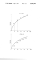
- FIG. 1 is a characteristic diagram useful in explaining the principles of a logarithmic function generating system according to the invention.
- FIG. 2 is a time-voltage characteristic diagram useful for explaining the principles of the system of this invention.
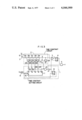
- FIG. 3 is a wiring diagram showing an embodiment of the system of this invention.
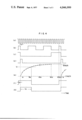
- FIG. 4 is a waveform diagram useful for explaining the operation of the system of this invention.
- numeral 1 designates a time constant setting circuit for generating a setting signal corresponding to the number of input pulse signals, 2 a resistance-capacitance time constant circuit (hereinafter simply referred to as an RC charging circuit) whose time constant varies in accordance with the output setting signal of the time constant setting circuit 1.
- RC charging circuit resistance-capacitance time constant circuit
- the time constant setting circuit 1 comprises a binary counter 11 (such as the Motorola MC 14040), inverters 12a, 12b, 12c and 12d respectively connected to the first-position to fourth-position outputs Q 1 , Q 2 , Q 3 and Q 4 of the binary counter 11, a NAND gate 13 for receiving as its inputs the third-position output Q 3 and fifth-position output Q 5 of the binary counter 11, an inverter 14 for inverting the output of the NAND gate 13, a D-type flip-flop 15 for delaying the output of the NAND gate 13 and applying it to a reset terminal R of the binary counter 11 and an inverter 16 connected to a clock input terminal CL of the binary counter 11.
- a binary counter 11 such as the Motorola MC 14040
- inverters 12a, 12b, 12c and 12d respectively connected to the first-position to fourth-position outputs Q 1 , Q 2 , Q 3 and Q 4 of the binary counter 11
- a NAND gate 13 for receiving as its inputs the third-position output Q 3 and fifth-
- the RC charging circuit 2 comprises series-connected resistors 21a and 21b of a resistance value R, resistor 21c of a resistance value 2R, resistor 21d of a resistance value 4R and resistor 21e of a resistance value 8R, analog switches 22a, 22b, 22c and 22d (such as the RCA CD4016) respectively connected to the ends of the resistors 21b, 21c, 21d and 21e and disposed to receive as their control inputs the outputs of the inverters 12a to 12d, respectively, a capacitor 23 having a capacitance value C and connected to the end of the resistor 21e and an analog switch 24 connected in parallel with the capacitor 23 and disposed to receive as its control input the fifth-position output Q 5 of the binary counter 11.
- Numerals 6, 7 and 8 designate terminals for respectively receiving a preset voltage V i , constant voltage V c and clock signals of a predetermined frequency.
- a comparator 3 an R-S flip-flop 4 and an AND gate 5 so that a pulse signal of a time width bearing a logarithmic relation to the preset voltage V i applied to the terminal 6 is generated.
- the time constant of the RC charging circuit 2 is increased in proportion to the time expired, thus increasing the time constant from RC to 2RC, 3RC, . . . , 16RC.
- the voltage waveform generated at the point X consists of 16 interconnected charging curves with different time constants and it is evident that as previously noted this voltage waveform approximately realizes the broken line approximation to the logarithmic function which is shown by the dotted lines in FIG. 1.
- the output of the NAND gate 13 is inverted by the inverter 14, delayed by one clock period or unit time t 0 and then applied to the reset terminal R of the binary counter 11.
- the binary counter 11 is reset clearing all of its outputs Q 1 to Q 5 to "0" and restoring the initial conditions and the RC charing circuit 2 starts again its charging action with the time constants RC, 2RC, 3RC, . . . .
- the inverter 16 is connected to the clock input terminal CL of the binary counter 11 to adjust the phase relationships between the binary counter 11 and the D-type flip-flop 15 since the binary counter 11 counts the applied clock signals at their falling edges and the D-type flip-flop 15 changes its state in response to the rising edges of the clock signals.
- the point X is also connected to the noninverting input of the comparator 3 which compares the voltage at the point X with the preset voltage V i which is applied to its inverting input. Since the output of the comparator 3 is connected to a reset terminal R of the R-S flip-flop 4 and the output of the inverter 14 is connected to the set input terminal of the R-S flip-flop 4, when the count value of the binary counter 11 reaches 20 so that the third-position output Q 3 and the fifth-position output Q 5 go to "1", the output of the inverter 14 goes to "1" and the R-S flip-flop 4 is set causing its Q output to go to "1” as shown in (f) of FIG. 4.
- the R-S flip-flop 4 serves to prevent the occurrence of a chattering phenomenon to the output of the comparator 3 due to the effect of the accuracy of detection or the response characteristics of the comparator 3. In other words, once a "1" has been applied to the reset input R of the R-S flip-flop 4 changing its Q output to "0", the Q output remains in the same state until a "1" is applied to the set input S and in this way any chattering produced in the output of the comparator 3 is cancelled.
- the slope of the tangent is no longer inversely proportional to the time and slopes gradually deviate from the broken line shown by the dotted lines in FIG. 1.
- the frequency of clock signals and the constant voltage V c are respectively selected 4096 Hz and 6 V, with a specified time constant, the resulting approximation errors with respect to the computed values would be less than ⁇ 3% under a range 200 ( ⁇ sec) ⁇ t Q ⁇ 3.5 (m sec), making it possible to produce with a sufficiently high degree of accuracy a logarithmic function voltage with a time as a variable and put it to practical use.
- the desired approximation accuracy may be obtained even if the predetermined time constant is decreased, while the similar approximation accuracy may be obtained by setting the frequency and the time constant conversely. Still further, it is possible to correct the previously mentioned deviations with the lapse of time so as to ensure the desired approximation accuracy over a wide range of intervals.
- those elements which involve the problem of nonuniformity of characteristics or the problem of temperature characteristics are only the resistors 21a through 21e and the capacitor 23 constituting the RC charging circuit 2.
- the ordinary resistors such as metal film resistors which are stable and highly accurate with a variation of about ⁇ 1% and a temperature coefficient of ⁇ 50 ppm/° C. are available.
- the ordinary type capacitors such as, ceramic capacitors and polyester film capacitors whose temperature coefficients are almost zero are available.
- analog switches 22a through 22d are controlled to change the time constant of the RC charging circuit 2, this control may be accomplished with only the binary counter 11 and the inverters 12a through 12d simplifying the circuitry considerably. Still further, since a pulse of the time width t Q can be easily generated, it is possible to easily obtain the number of clock pulses proportional to the output pulse width t Q through such an operation by which the number of clock signals applied during the time width t Q is counted and thus the system of this invention may be made to serve such functions as served by analog-to-digital converters.
- the desired logarithmic function voltage is approximated with 16 RC charging curves having different time constants, by increasing the number of bit positions in the binary counter 11 and adding as many analog switches and resistors as desired to the analog switches 22a and 22d and the resistors 21a to 21e, it is possible to approximate with increased accuracy the desired logarithmic function voltage with a broken line including a greater number of segments.
- the RC charging circuit 2 is designed to change its time constant by varying the resistance value, it is possible to arrange so that a plurality of capacitors are similarly controlled by means of analog switches to vary the total capacitance and thereby to change the time constant.
- the time constant for each interval may be determined by means of the single resistor or capacitor and therefore it is possible to generate with greater accuracy the desired logarithmic function voltage with a time as a variable by strictly adjusting the resistance values or capacitance values.
- the resistance-capacitance (R-C) time constant circuit may be replaced by a resistance-inductance (R-L) time constant circuit as well without departing from the scope of this invention.
Applications Claiming Priority (2)
| Application Number | Priority Date | Filing Date | Title |
|---|---|---|---|
| JA50-72892 | 1975-06-16 | ||
| JP50072892A JPS51148341A (en) | 1975-06-16 | 1975-06-16 | Logarithm function generator |
Publications (1)
| Publication Number | Publication Date |
|---|---|
| US4046999A true US4046999A (en) | 1977-09-06 |
Family
ID=13502443
Family Applications (1)
| Application Number | Title | Priority Date | Filing Date |
|---|---|---|---|
| US05/681,744 Expired - Lifetime US4046999A (en) | 1975-06-16 | 1976-04-29 | Logarithmic function generating system |
Country Status (3)
| Country | Link |
|---|---|
| US (1) | US4046999A (de) |
| JP (1) | JPS51148341A (de) |
| DE (1) | DE2621849C2 (de) |
Cited By (5)
| Publication number | Priority date | Publication date | Assignee | Title |
|---|---|---|---|---|
| US4362995A (en) * | 1980-01-08 | 1982-12-07 | Northern Telecom, Inc. | Method of and apparatus for producing a logarithmic representation of an input voltage |
| US5197024A (en) * | 1989-06-14 | 1993-03-23 | Pickett Lester C | Method and apparatus for exponential/logarithmic computation |
| WO1994018633A1 (en) * | 1991-01-30 | 1994-08-18 | Lester Caryl Pickett | High speed function generating apparatus and method |
| WO1994018632A1 (en) * | 1993-02-01 | 1994-08-18 | Lester Caryl Pickett | Low latency function generating apparatus and method |
| US10331571B2 (en) * | 2016-08-12 | 2019-06-25 | Minebea Mitsumi Inc. | Address control circuit capable of setting address rapidly and method of setting address after power-on reset, the address control circuit providing protection against over-voltage |
Citations (5)
| Publication number | Priority date | Publication date | Assignee | Title |
|---|---|---|---|---|
| US3579127A (en) * | 1967-05-31 | 1971-05-18 | Gulf Energy & Environ Systems | Apparatus for monitoring pulses |
| US3649826A (en) * | 1969-12-22 | 1972-03-14 | Corning Glass Works | Integrating antilog function generator |
| US3805046A (en) * | 1972-12-11 | 1974-04-16 | Spectra Physics | Logarithmic conversion system |
| US3828255A (en) * | 1971-08-05 | 1974-08-06 | Wandel & Goltermann | Electric meter with logarithmically indicating digital reader |
| US3878383A (en) * | 1972-02-02 | 1975-04-15 | Iwatsu Electric Co Ltd | System for converting a ratio of two signals into a logarithmic value |
Family Cites Families (1)
| Publication number | Priority date | Publication date | Assignee | Title |
|---|---|---|---|---|
| DE2446629A1 (de) * | 1974-09-19 | 1976-04-15 | Siemens Ag | Funktionsgenerator |
-
1975
- 1975-06-16 JP JP50072892A patent/JPS51148341A/ja active Granted
-
1976
- 1976-04-29 US US05/681,744 patent/US4046999A/en not_active Expired - Lifetime
- 1976-05-17 DE DE2621849A patent/DE2621849C2/de not_active Expired
Patent Citations (5)
| Publication number | Priority date | Publication date | Assignee | Title |
|---|---|---|---|---|
| US3579127A (en) * | 1967-05-31 | 1971-05-18 | Gulf Energy & Environ Systems | Apparatus for monitoring pulses |
| US3649826A (en) * | 1969-12-22 | 1972-03-14 | Corning Glass Works | Integrating antilog function generator |
| US3828255A (en) * | 1971-08-05 | 1974-08-06 | Wandel & Goltermann | Electric meter with logarithmically indicating digital reader |
| US3878383A (en) * | 1972-02-02 | 1975-04-15 | Iwatsu Electric Co Ltd | System for converting a ratio of two signals into a logarithmic value |
| US3805046A (en) * | 1972-12-11 | 1974-04-16 | Spectra Physics | Logarithmic conversion system |
Cited By (6)
| Publication number | Priority date | Publication date | Assignee | Title |
|---|---|---|---|---|
| US4362995A (en) * | 1980-01-08 | 1982-12-07 | Northern Telecom, Inc. | Method of and apparatus for producing a logarithmic representation of an input voltage |
| US5197024A (en) * | 1989-06-14 | 1993-03-23 | Pickett Lester C | Method and apparatus for exponential/logarithmic computation |
| US5359551A (en) * | 1989-06-14 | 1994-10-25 | Log Point Technologies, Inc. | High speed logarithmic function generating apparatus |
| WO1994018633A1 (en) * | 1991-01-30 | 1994-08-18 | Lester Caryl Pickett | High speed function generating apparatus and method |
| WO1994018632A1 (en) * | 1993-02-01 | 1994-08-18 | Lester Caryl Pickett | Low latency function generating apparatus and method |
| US10331571B2 (en) * | 2016-08-12 | 2019-06-25 | Minebea Mitsumi Inc. | Address control circuit capable of setting address rapidly and method of setting address after power-on reset, the address control circuit providing protection against over-voltage |
Also Published As
| Publication number | Publication date |
|---|---|
| DE2621849A1 (de) | 1976-12-23 |
| JPS51148341A (en) | 1976-12-20 |
| JPS5722144B2 (de) | 1982-05-11 |
| DE2621849C2 (de) | 1982-08-26 |
Similar Documents
| Publication | Publication Date | Title |
|---|---|---|
| US5513235A (en) | Integrated circuit thermometer | |
| EP0805579B1 (de) | Demodulator für ein pulsbreitenmoduliertes Signal | |
| US4544911A (en) | Low cost monotonic digital-to-analog converter | |
| US4046999A (en) | Logarithmic function generating system | |
| US3914623A (en) | Waveform generator including means for automatic slope calibration | |
| US4296407A (en) | Digital frequency synthesizer with frequency divider programmable in response to stored digital control signal | |
| EP0525798A2 (de) | Integrierter Abtast-Halte-Phasendetektor mit einem stromeinstellenden integrierten Widerstand | |
| KR920008051B1 (ko) | 디지탈-아나로그 변환기 장치 | |
| US3809874A (en) | Device for calculating the mean value of a succession of data | |
| US4504741A (en) | Digital circuit for generating ascending or descending ramp-like waveforms | |
| US4559521A (en) | Calibration of a multi-slope A-D converter | |
| US5220219A (en) | Electronically controlled variable gain amplifier | |
| US4389637A (en) | Digital to analog converter | |
| US3916179A (en) | Electronic integrator with voltage controlled time constant | |
| US4623800A (en) | Clock controlled dual slope voltage to frequency converter | |
| US4184151A (en) | Circuit for digitally processing exposure information | |
| EP0535124B1 (de) | Analog-digitalumsetzer | |
| US4352206A (en) | Comparison arrangement for a digital tuning system | |
| EP0162496A1 (de) | Phasenriegelschleife mit einem schaltenden Phasendetektor | |
| US3983369A (en) | Digital hyperbolic function generator | |
| GB2073981A (en) | Frequency comparison arrangement for a digital tuning system | |
| US4146836A (en) | Power monitor | |
| US4321548A (en) | Frequency-voltage and voltage-frequency converters | |
| JPS5911151B2 (ja) | デジタル式対数関数発生装置 | |
| JPS628052B2 (de) |